Inrush limiter also provides short-circuit protection ... - EDN.com
Inrush limiter also provides short-circuit protection ... - EDN.com
Inrush limiter also provides short-circuit protection ... - EDN.com

Create successful ePaper yourself
Turn your PDF publications into a flip-book with our unique Google optimized e-Paper software.
designideas<br />
EDITED BY BRAD THOMPSON<br />
AND FRAN GRANVILLE<br />
READERS SOLVE DESIGN PROBLEMS<br />
<strong>Inrush</strong> <strong>limiter</strong> <strong>also</strong> <strong>provides</strong><br />
<strong>short</strong>-<strong>circuit</strong> <strong>protection</strong><br />
Ryan Brownlee, Process Automation Division,<br />
Pepperl & Fuchs Inc, Twinsburg, OH<br />
<br />
For containing large amounts of<br />
bulk capacitance, controlling<br />
inrush currents poses problems. The<br />
simplest approach involves placing an<br />
inrush-limiting resistor in series with<br />
the capacitor bank, but a resistor wastes<br />
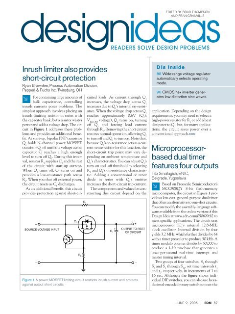
power and adds a voltage drop. The <strong>circuit</strong><br />
in Figure 1 addresses these problems<br />
and <strong>provides</strong> an additional benefit.<br />
At start-up, bipolar PNP transistor<br />
Q 2 holds N-channel power MOSFET<br />
transistor Q 1 off until the voltage across<br />
capacitor C l reaches a high enough<br />
level to turn off Q 2 . During this interval,<br />
resistor R 1 supplies C 1 and the rest<br />
of the <strong>circuit</strong> with start-up current.<br />
When Q 2 turns off, Q 1 turns on and<br />
<strong>provides</strong> a low-resistance path across<br />
R 1 . When you shut off external power,<br />
the <strong>circuit</strong> resets as C 1 discharges.<br />
As an additional benefit, this <strong>circuit</strong><br />
<strong>provides</strong> <strong>protection</strong> against <strong>short</strong>-cir-<br />
+<br />
SOURCE-VOLTAGE INPUT<br />
<br />
Q 2<br />
Q 1<br />
R 3<br />
cuited loads. As current through Q 1<br />
increases, the voltage drop across Q 1<br />
increases due to Q 1 ’s internal on-resistance.<br />
When the voltage drop across Q 1<br />
reaches approximately 0.6V (Q 2 ’s<br />
V BE(ON) voltage), Q 2 turns on, turning<br />
off Q 1 and forcing load current<br />
through R 1 . Removing the <strong>short</strong> <strong>circuit</strong><br />
restores normal operation, allowing Q 2<br />
to turn off and Q 1 to turn on. Note that,<br />
because Q 1 ’s on-resistance acts as a current-sense<br />
resistor for this function, the<br />
<strong>short</strong>-<strong>circuit</strong> trip point may vary depending<br />
on ambient temperature and<br />
Q 1 ’s characteristics. You can adjust Q 1 ’s<br />
turn-on and -off threshold by selecting<br />
R 1 and Q 1 ’s on-resistance characteristic.<br />
Adding a conventional or zener<br />
diode in series with Q 2 ’s emitter<br />
increases the <strong>short</strong>-<strong>circuit</strong> trip current.<br />
The <strong>com</strong>ponents and values for constructing<br />
this <strong>circuit</strong> depend on the<br />
Figure 1 A power-MOSFET-limiting <strong>circuit</strong> restricts inrush current and protects<br />
against output <strong>short</strong> <strong>circuit</strong>s.<br />
R 1<br />
+<br />
C1 +<br />
OUTPUT TO REST<br />
OF CIRCUIT<br />
<br />
DIs Inside<br />
88 Wide-range voltage regulator<br />
automatically selects operating<br />
mode.<br />
90 CMOS hex inverter generates<br />
low-distortion sine waves.<br />
application. Depending on the design<br />
requirements, you may need to select a<br />
high-power resistor for R 1 or add a heat<br />
dissipater to Q 1 , but, for many applications,<br />
the <strong>circuit</strong> saves power over a<br />
conventional approach.<strong>EDN</strong><br />
Microprocessorbased<br />
dual timer<br />
features four outputs<br />
Tito Smailagich, ENIC,<br />
Belgrade, Yugoslavia<br />
Based on Freescale Semiconductor’s<br />
MCC908QY 8-bit flash-memory<br />
micro<strong>com</strong>puter, the <strong>circuit</strong> in Figure 1 <strong>provides</strong><br />
a low-cost, general-purpose dual timer<br />
that offers an alternative to one-shot <strong>circuit</strong>s.<br />
You can modify the assembly-language software<br />
available from the online version of this<br />
Design Idea at www.edn.<strong>com</strong>/050609di2 to<br />
meet specific applications. The <strong>circuit</strong> uses<br />
microprocessor IC ’s internal 12.8-MHz<br />
1<br />
clock oscillator. Internal division by four<br />
yields 3.2 MHz, which further divides by 64<br />
with a timer prescaler to produce 50 kHz. A<br />
timer modulo counter divides by 50,000 to<br />
produce a 1-Hz timebase that generates a<br />
once-per-second real-time interrupt and<br />
master timing interval.<br />
Two groups of four switches, S through<br />
3<br />
S and S through S , set time intervals t 6 7 10 1<br />
and t , respectively, in increments of 1 to<br />
2<br />
16 sec. Although the figure shows individual<br />
DIP switches, you can <strong>also</strong> use hexadecimal-encoded<br />
rotary switches to set the<br />
JUNE 9, 2005 | <strong>EDN</strong> 87
designideas<br />
START1<br />
STOP 1<br />
S 1<br />
S 2<br />
Figure 1 This dual timer <strong>com</strong>prises only a few switches and a microprocessor<br />
whose internal clock sets the time intervals.<br />
time intervals. For demonstration purposes,<br />
LEDs D 1 through D 4 show the<br />
outputs’ states during the timing cycle.<br />
Normally open pushbutton switches S 1<br />
The <strong>circuit</strong> in Figure 1 delivers<br />
programming voltages to an<br />
EEPROM under the control of an<br />
external DAC (not shown). You can<br />
replace the DAC with a potentiometer<br />
to create a general-purpose power supply<br />
operating from 12V and able to<br />
deliver a variable output voltage of 0 to<br />
32V. As Figure 1 shows, a Linear<br />
Technology LT1072HV variable-boost<br />
switching regulator, IC , drives a Class<br />
1<br />
A amplifier <strong>com</strong>prising operational<br />
amplifier IC , voltage-boost-stage Q ,<br />
2 3<br />
and emitter-follower Darlington transistor<br />
Q . Resistors R and R set the<br />
2 9 10<br />
amplifier’s noninverting loop gain to<br />
a value of 1(R /R ). 9 10<br />
and S 2 start and stop the timers’ operating<br />
cycles. The start function initiates<br />
the main timer and operates only when<br />
the timer stops. After activation, out-<br />
Wide-range voltage regulator<br />
automatically selects operating mode<br />
Joel Setton, Crolles, France<br />
88 <strong>EDN</strong> | JUNE 9, 2005<br />
2<br />
2<br />
9<br />
8<br />
PA2<br />
PA3<br />
2 3 6 7 10 11 14 15<br />
2<br />
S 3<br />
2<br />
S 4<br />
R 1<br />
1.22k<br />
PB7 PB6 PB5 PB4 PB3 PB2 PB1 PB0<br />
2<br />
S 5<br />
T 1<br />
R 2<br />
1.22k<br />
IC 1<br />
MC908QY<br />
2<br />
S 6<br />
1 1 1 1 1 1 1 1<br />
B3 B2 B1 B0 B3 B2 B1 B0 2<br />
S 7<br />
T 2<br />
1 1 1 1<br />
R 3<br />
1.22k<br />
D1 D2 D3 D4 1 1 1 1<br />
Q1 Q2 Q3 Q4 13 12 5 4<br />
PA0 PA1 PA4 PA5<br />
2<br />
S 8<br />
R 4<br />
1.22k<br />
T 1 SETUP T 2 SETUP<br />
2<br />
S 9<br />
1<br />
VDD<br />
16<br />
VSS<br />
2<br />
S 10<br />
5V<br />
V CC<br />
1 C1 2<br />
0.1 F<br />
For output voltages below 8V, switching<br />
regulator IC 1 remains in shutdown<br />
mode, and the output stage draws current<br />
through L 1 and D 1 . Q 1 ’s collector<br />
voltage, V C , measures approximately<br />
11.4V—that is, 12V minus D 1 ’s forward-voltage<br />
drop. Transistor Q 1 monitors<br />
the voltage drop across R 7 , which<br />
measures a fraction of Q 2 ’s collectorbase<br />
voltage, V CB . As long as V CB<br />
exceeds 1V, Q 1 ’s collector current<br />
remains high enough to drive IC 1 ’s feedback<br />
input higher than 1.25V, which in<br />
turn keeps IC 1 shut down.<br />
As the output voltage increases, the<br />
voltage differential across R 7 decreases,<br />
and, when it drops below 0.9V, Q 1 ’s col-<br />
OUTPUTS<br />
START<br />
SWITCH<br />
CLOSURE<br />
Q 1<br />
Q 2<br />
Q 3<br />
Q 4<br />
Figure 2 This timing diagram illustrates<br />
outputs available from the timer’s two<br />
sections.<br />
put Q 1 goes to logic one during interval<br />
t 1 (Figure 2). Output Q 2 <strong>com</strong>plements<br />
Q 1 and remains at logic one until<br />
the next cycle starts. On Q 1 ’s trailing<br />
edge, output Q 3 goes to logic one for<br />
time interval t 2 . After t 2 elapses, output<br />
Q 4 goes to logic one and remains there<br />
until the next cycle starts. You can use<br />
the stop switch, S 2 , at any time to terminate<br />
a cycle and reset all four outputs<br />
to logic one.<strong>EDN</strong><br />
lector current decreases, lowering the<br />
feedback voltage applied to IC 1 and<br />
switching it on. The boost regulator’s<br />
output voltage increases, and the Q 1 -<br />
IC 1 feedback loop regulates the collector-emitter<br />
voltage differential across<br />
Q 2 to a constant 3V for all outputs<br />
exceeding 8V. If IC 2 ’s output goes to<br />
ground, cutting off Q 3 and forcing Q 2<br />
into saturation, the feedback loop<br />
around Q 1 opens and allows the <strong>circuit</strong>’s<br />
output voltage to increase. Diode D 5<br />
and associated <strong>com</strong>ponents form an<br />
overvoltage-<strong>protection</strong> clamp that limits<br />
IC 1 ’s output to 37V.<br />
Resistive divider R 9 and R 10 and IC 2<br />
determine the output voltage’s range.<br />
t 1<br />
t 2
designideas<br />
Apart from selecting the V CE ratings of<br />
Q 1 and Q 3 to withstand the highest<br />
desired output voltage, values of other<br />
12V<br />
SUPPLY<br />
C 1<br />
100 F<br />
25V<br />
<strong>com</strong>ponents are not critical. If you substitute<br />
appropriate <strong>com</strong>ponents for D 5 ,<br />
Q 1 , and Q 3 , the <strong>circuit</strong> can deliver out-<br />
put voltages as high as IC 1 ’s maximum<br />
output-switch rating—75V for the<br />
LT1072HV variant—minus 3V.<strong>EDN</strong><br />
Figure 1 Able to deliver a wide range of output voltages, this regulator <strong>circuit</strong> automatically selects a linear or a switched mode<br />
as required.<br />
CMOS hex inverter generates<br />
low-distortion sine waves<br />
Al Dutcher, West Deptford, NJ<br />
<br />
+<br />
C 2<br />
0.22 F<br />
R 1<br />
1.5k<br />
This Design Idea <strong>provides</strong> a simple,<br />
inexpensive, portable <strong>circuit</strong><br />
as an alternative to a microcontroller<br />
to provide a wide-range source of lowdistortion<br />
sine waves for audio-<strong>circuit</strong><br />
design and debugging. Although sine<br />
waves from DDS (direct digital synthesis)<br />
offer greater stability and fewer<br />
harmonics and other spurious-frequency<br />
<strong>com</strong>ponents, this more “retro”<br />
approach lets designers use Linear<br />
Technology Corp’s LTSpice freeware<br />
and hone their <strong>circuit</strong>-simulation<br />
skills. An oscillator <strong>com</strong>prises a frequency-determining<br />
network and a<br />
90 <strong>EDN</strong> | JUNE 9, 2005<br />
L 1<br />
220 H<br />
V IN<br />
V C<br />
IC 1<br />
LT1072HV<br />
GND<br />
V SW<br />
FB<br />
R 3<br />
10k<br />
D 1<br />
1N4936<br />
R 2<br />
1k<br />
D5 36V<br />
D2 1N4148<br />
0 TO 2V<br />
CONTROL INPUT<br />
FROM DAC<br />
R 10<br />
1k<br />
C 3<br />
22 F<br />
63V<br />
R 4<br />
10k<br />
method of limiting oscillation amplitude<br />
to prevent <strong>circuit</strong> saturation,<br />
waveform clipping, and the generation<br />
of harmonics. Many audio-oscillator<br />
designs use classic Wien-bridge bandpass-filter<br />
topology and include incandescent<br />
lamps, thermistors, or JFET <strong>circuit</strong>s<br />
as amplitude-sensitive resistors to<br />
automatically vary feedback and limit<br />
amplitude.<br />
However, amplitude-sensitive resistors<br />
introduce a small delay that can<br />
cause amplitude ringing while the oscillator<br />
stabilizes. In addition, the <strong>limiter</strong>’s<br />
“soft” characteristics require fre-<br />
+<br />
IC2 ½LM358<br />
_<br />
+<br />
R 6<br />
3.3k<br />
D 3<br />
1N4148<br />
Q 1<br />
2N5087<br />
R 9<br />
15k<br />
R 11<br />
10k<br />
R 12<br />
4.7k<br />
R 7<br />
4.7k<br />
R 8<br />
4.7k<br />
R 13<br />
100<br />
C 4<br />
100 nF<br />
Q 3<br />
BC237<br />
V C<br />
Q 2<br />
MPS-U45<br />
D 4<br />
1N4148 OUTPUT<br />
0 TO 32V<br />
quency-determining <strong>com</strong>ponents that<br />
track closely and maintain a level amplitude<br />
response over the oscillation<br />
range. Diode <strong>limiter</strong>s present a softer<br />
characteristic than allowing an amplifier<br />
to go into “hard” limiting, and a<br />
diode <strong>limiter</strong> introduces no envelope<br />
delay. A Wien-bridge filter’s frequency<br />
response rolls off relatively slowly and<br />
thus inadequately rejects clipping-induced<br />
harmonic frequencies. As a consequence,<br />
designers of most high-quality<br />
oscillators eschew the use of<br />
hard-clipping <strong>limiter</strong>s.<br />
Figure 1 shows a sine-wave-oscilla-
designideas<br />
R 10<br />
15k<br />
R 11<br />
150k<br />
tor design that makes unconventional<br />
use of a logic <strong>circuit</strong>. Based on statevariable<br />
topology that <strong>provides</strong> buffered<br />
highpass-, bandpass-, and lowpass-filtering<br />
nodes in one <strong>circuit</strong>, this<br />
oscillator relies on the peaking characteristics<br />
of an underdamped, two-pole<br />
lowpass filter that significantly boosts<br />
response at the fundamental frequency.<br />
In addition, the filter’s lowpass node<br />
<strong>provides</strong> 12-dB-per-octave attenuation<br />
for harmonics. The state-variable<br />
loop <strong>com</strong>prises two integrators and a<br />
summing amplifier that <strong>provides</strong> 180<br />
of phase shift. The two integrators each<br />
add almost 90 of additional phase<br />
shift, and the whole loop thus presents<br />
slightly less than 360 or 0 of phase shift<br />
and unity gain for oscillation.<br />
The loop’s gain blocks <strong>com</strong>prise un-<br />
92 <strong>EDN</strong> | JUNE 9, 2005<br />
D 1<br />
1N4148<br />
D 2<br />
1N4148<br />
FIRST INTEGRATOR<br />
RV 2<br />
0 TO 100k<br />
IC 1D<br />
IC 1A<br />
C1<br />
R 3<br />
3.3k<br />
R 1<br />
68<br />
BANDPASS<br />
FILTER<br />
R 12<br />
15k<br />
R 6<br />
3.3k<br />
R 2<br />
3.3k<br />
SCHMIDT TRIGGER<br />
S 1<br />
NOTE: IC 1 =74HCU04 HEX INVERTER.<br />
+<br />
V<br />
V+<br />
RV 1<br />
0 TO 100k<br />
SQUARE-WAVE OUTPUT<br />
SINE-WAVE OUTPUT<br />
5V<br />
LIMITER<br />
SECOND INTEGRATOR<br />
IC 1E<br />
R 13<br />
15k<br />
C 2<br />
IC 1B<br />
LOWPASS<br />
FILTER<br />
V<br />
buffered 74HCU04 CMOS inverters<br />
that emphasize <strong>circuit</strong> simplicity, wide<br />
bandwidth, and self-referencing logic<br />
thresholds. Individual inverters each<br />
provide relatively low-voltage gains of<br />
approximately 15 per stage. Operating<br />
in Class A linear mode, the inverters<br />
produce no crossover distortion and<br />
thus produce harmonic amplitudes<br />
that decrease rapidly with harmonic<br />
order. In addition, a 74HCU04 package<br />
contains six inverters, making possible<br />
a one-device oscillator <strong>circuit</strong>.<br />
To understand how the <strong>circuit</strong> operates,<br />
use the summing node at IC 1C ’s input<br />
as a phase reference. Summing amplifier<br />
IC 1C <strong>provides</strong> the first 180 of<br />
phase shift (inversion). Inverter/integrators<br />
IC 1A and IC 1B each present a<br />
quality factor, Q, equal to a gain of ap-<br />
R 7<br />
68k<br />
C 3<br />
5 pF<br />
R 4<br />
15k<br />
R 8<br />
15k<br />
SINE-WAVE OUTPUT<br />
GND<br />
SUM<br />
R 9<br />
150k<br />
IC 1F<br />
IC 1C<br />
VIRTUAL-GROUND SOURCE<br />
C4 330 F<br />
+<br />
C5 330 F<br />
+<br />
SUMMING<br />
AMPLIFIER<br />
R5 HIGHPASS<br />
15k FILTER<br />
Figure 1 Build a sine-wave source around a single high-speed CMOS hex inverter and a handful of <strong>com</strong>ponents.<br />
proximately 15, contributing a phase<br />
shift of 86 for a total of 1808694<br />
each. The total phase margin for the<br />
three stages is 18094948 degrees.<br />
The <strong>circuit</strong>’s phase shift now<br />
amounts to 8 away from the “perfect”<br />
0 phase required for oscillation. The<br />
total <strong>circuit</strong> Q of approximately 7.5<br />
<strong>provides</strong> a boosted fundamental-frequency-filtering<br />
action of approximately<br />
17 dB, but, at 8 phase shift, the<br />
<strong>circuit</strong> does not oscillate.<br />
To obtain the exact 360 phase shift<br />
for oscillation, apply a small amount of<br />
signal from the filter’s bandpass tap,<br />
which operates at a phase angle of<br />
1801808686. Combine the<br />
<strong>circuit</strong>’s Q of 7.5 and attenuate the<br />
bandpass intermediate output’s signal<br />
at the bandpass filter by a factor of four,
designideas<br />
and the <strong>circuit</strong> oscillates with adequate<br />
gain and phase margins. Due to its<br />
symmetric internal configuration, a<br />
CMOS-inverter <strong>circuit</strong> attempts to<br />
maintain a logic threshold of one-half<br />
of its supply voltage. However, an Nchannel<br />
MOS transistor conducts<br />
more than its P-channel counterpart,<br />
and the logic threshold shifts slightly<br />
toward the negative supply rail. Because<br />
an imbalance would lead to<br />
asymmetry if you use it as is for limiting<br />
the oscillation’s amplitude, a pair of<br />
back-to-back 1N4148 diodes, D 1 and<br />
D 2 , serves as a symmetrical <strong>limiter</strong>, preventing<br />
the gates from clipping the<br />
bandpass filter’s output.<br />
Soft clipping eases the filter’s performance<br />
requirements by producing<br />
a third-harmonic level of 17 dB at the<br />
clipper’s output. The filter’s response<br />
peaks at 17 dB at the oscillation frequency,<br />
and the lowpass node <strong>provides</strong><br />
20 dB of third-harmonic attenuation<br />
for a theoretical third-harmonic total<br />
rejection of 54 dB. In practice, the<br />
CMOS devices’ gain and threshold<br />
characteristics depart from ideal performance,<br />
and, as a result, the <strong>circuit</strong><br />
produces sine waves that approach 1%<br />
distortion at the lowpass node, an acceptable<br />
level for the intended application.<br />
Replacing the CMOS inverters<br />
with operational amplifiers would further<br />
enhance performance.<br />
The filter’s highpass node <strong>provides</strong><br />
the first integrator’s input signal, and<br />
the two cascaded integrators approach<br />
a 180 phase shift for all frequency<br />
<strong>com</strong>ponents and <strong>also</strong> attenuate harmonic<br />
frequencies by a factor of 1/N 2 ,<br />
where N represents the harmonic<br />
number. Subtracting some of the highpass<br />
signal, which contains harmonics<br />
produced by the diode <strong>limiter</strong>, from the<br />
lowpass signal further reduces the output’s<br />
harmonic <strong>com</strong>ponents. Resistors<br />
R 8 and R 9 form a 10-to-1 cancellation<br />
<strong>circuit</strong> that <strong>provides</strong> an additional 6-dB<br />
harmonic reduction for a 0.5% distortion<br />
figure at the signal output. Figure<br />
2 shows harmonic levels for a 500-Hz<br />
fundamental output frequency.<br />
Oscillation occurs at unity gain at<br />
which the integrator’s capacitive reactance<br />
equals the integrator’s resistance,<br />
94 <strong>EDN</strong> | JUNE 9, 2005<br />
V OUT<br />
(dB)<br />
0<br />
10<br />
20<br />
30<br />
40<br />
50<br />
60<br />
70<br />
80<br />
90<br />
100<br />
110<br />
50.0082 500.082 5.00082k<br />
Figure 2 The oscillator’s output spectrum contains second- and third-harmonic<br />
levels of at least 250 dB below the fundamental.<br />
and at a frequency of 1/(2RC),<br />
where R = (RV 1 R 2 )(RV 2 R 3 ), and<br />
CC 1 C 2 .For C10 nF and values of<br />
R of 8 to 80 k, the <strong>circuit</strong> produces<br />
frequencies of 200 Hz to 2 kHz. You<br />
can use a 100-k, dual-section ganged<br />
stereo-audio potentiometer as a frequency<br />
control. The control’s ganged<br />
sections ensure that the integrators’ resistance<br />
elements adequately track<br />
each other. To cover the audio spectrum<br />
of 2 Hz to 200 kHz, add a twosection<br />
band switch (not shown) to select<br />
pairs of capacitors with values of<br />
1 F, 100 nF, 10 nF, 1 nF, and 100 pF.<br />
You can use matched pairs of temperature-stable<br />
ceramic capacitors, but<br />
film-dielectric capacitors improve frequency<br />
stability. Compensation capacitor<br />
C 3 improves output flatness at<br />
higher frequencies. Over a typical frequency<br />
band, the output amplitude remains<br />
flat within 1 dB.<br />
One of IC 1 ’s three remaining inverters,<br />
IC 1F , serves as a virtual-ground<br />
generator by dividing the 5V power<br />
supply, a floating four-cell stack of AAsized<br />
nickel-cadmium or nickel-metalhydride<br />
batteries. Current drain from<br />
the batteries averages 50 to 60 mA.<br />
Switch S 1 connects the remaining inverters,<br />
IC 1D and IC 1E , to form a unity-<br />
FREQUENCY (Hz)<br />
gain buffer amplifier for sine-wave<br />
outputs or as a Schmidt trigger to produce<br />
a square-wave output. Resistor R 11<br />
sets the Schmidt trigger’s hysteresis level.<br />
For ease of construction, use a perforated<br />
prototype board and the DIP<br />
version of the 74HCU04.<br />
When you construct the <strong>circuit</strong>, note<br />
that the 74HCU04 can deliver appreciable<br />
gain at high frequencies, and excessively<br />
long leads can provoke parasitic<br />
oscillations that resistor R 1 helps<br />
suppress by reducing gain at frequencies<br />
in the very-high-frequency range.<br />
If you reduce <strong>circuit</strong> values, this oscillator<br />
easily operates in the high-frequency<br />
range, and, although its stability<br />
doesn’t approach that of an LCbased<br />
oscillator, the <strong>circuit</strong> offers easy<br />
adjustment over a wide frequency<br />
range.<strong>EDN</strong><br />
MORE AT <strong>EDN</strong>.COM<br />
+ For our Design Idea archive that<br />
goes back to 1994, visit www.edn.<br />
<strong>com</strong>/designideas.<br />
+<br />
And to see our “Best of Design<br />
Ideas” in 10 categories, check out<br />
www.edn.<strong>com</strong>/bestofdesignideas.