Demonstration of the Advantages of Electron Beam ... - Carl Zeiss SMT
Demonstration of the Advantages of Electron Beam ... - Carl Zeiss SMT
Demonstration of the Advantages of Electron Beam ... - Carl Zeiss SMT

You also want an ePaper? Increase the reach of your titles
YUMPU automatically turns print PDFs into web optimized ePapers that Google loves.
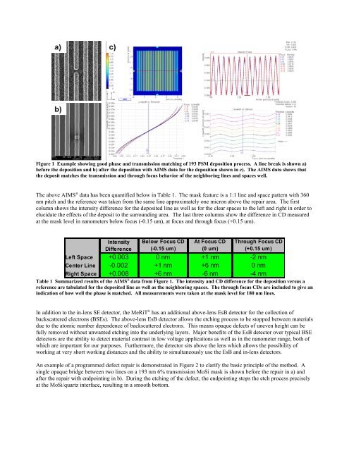
Figure 1 Example showing good phase and transmission matching <strong>of</strong> 193 PSM deposition process. A line break is shown a)<br />
before <strong>the</strong> deposition and b) after <strong>the</strong> deposition with AIMS data for <strong>the</strong> deposition shown in c). The AIMS data shows that<br />
<strong>the</strong> deposit matches <strong>the</strong> transmission and through focus behavior <strong>of</strong> <strong>the</strong> neighboring lines and spaces well.<br />
The above AIMS ® data has been quantified below in Table 1. The mask feature is a 1:1 line and space pattern with 360<br />
nm pitch and <strong>the</strong> reference was taken from <strong>the</strong> same line approximately one micron above <strong>the</strong> repair area. The first<br />
column shows <strong>the</strong> intensity difference for <strong>the</strong> deposited line as well as for <strong>the</strong> clear spaces to <strong>the</strong> left and right in order to<br />
elucidate <strong>the</strong> effects <strong>of</strong> <strong>the</strong> deposit to <strong>the</strong> surrounding area. The last three columns show <strong>the</strong> difference in CD measured<br />
at <strong>the</strong> mask level in nanometers below focus (-0.15 um), at focus and through focus (+0.15 um).<br />
Left Space<br />
Center Line<br />
Right Space<br />
Intensity Below Focus CD At Focus CD Through Focus CD<br />
Difference (-0.15 um) (0 um) (+0.15 um)<br />
+0.003<br />
-0.002<br />
+0.008<br />
0 nm<br />
+1 nm<br />
+6 nm<br />
+1 nm -2 nm<br />
+6 nm 0 nm<br />
-6 nm -4 nm<br />
Table 1 Summarized results <strong>of</strong> <strong>the</strong> AIMS ® data from Figure 1. The intensity and CD difference for <strong>the</strong> deposition versus a<br />
reference are tabulated for <strong>the</strong> deposited line as well as <strong>the</strong> neighboring spaces. The through focus CDs are included to give an<br />
indication <strong>of</strong> how well <strong>the</strong> phase is matched. All measurements were taken at <strong>the</strong> mask level for 180 nm lines.<br />
In addition to <strong>the</strong> in-lens SE detector, <strong>the</strong> MeRiT ® has an additional above-lens EsB detector for <strong>the</strong> collection <strong>of</strong><br />
backscattered electrons (BSEs). The above-lens EsB detector allows <strong>the</strong> etching process to be stopped between materials<br />
due to <strong>the</strong> atomic number dependence <strong>of</strong> backscattered electrons. This means opaque defects <strong>of</strong> uneven height can be<br />
fully removed without unwanted etching into <strong>the</strong> underlying layers. Major benefits <strong>of</strong> <strong>the</strong> EsB detector over typical BSE<br />
detectors are <strong>the</strong> ability to detect material contrast in low voltage applications as well as in <strong>the</strong> nanometer range, both <strong>of</strong><br />
which are important for our purposes. Fur<strong>the</strong>rmore, <strong>the</strong> detector sits above <strong>the</strong> lens which allows <strong>the</strong> possibility <strong>of</strong><br />
working at very short working distances and <strong>the</strong> ability to simultaneously use <strong>the</strong> EsB and in-lens detectors.<br />
An example <strong>of</strong> a programmed defect repair is demonstrated in Figure 2 to clarify <strong>the</strong> basic principle <strong>of</strong> <strong>the</strong> method. A<br />
single opaque bridge between two lines on a 193 nm 6% transmission MoSi mask is shown before <strong>the</strong> repair in a) and<br />
after <strong>the</strong> repair with endpointing in b). During <strong>the</strong> etching <strong>of</strong> <strong>the</strong> defect, <strong>the</strong> endpointing stops <strong>the</strong> etch process precisely<br />
at <strong>the</strong> MoSi/quartz interface, resulting in a smooth bottom.