CL7 Linear, 100mA, Constant Current LED Driver with ... - Supertex
CL7 Linear, 100mA, Constant Current LED Driver with ... - Supertex
CL7 Linear, 100mA, Constant Current LED Driver with ... - Supertex

You also want an ePaper? Increase the reach of your titles
YUMPU automatically turns print PDFs into web optimized ePapers that Google loves.
Features<br />
►<br />
►<br />
►<br />
►<br />
►<br />
►<br />
<strong>100mA</strong> ±5% constant current drive<br />
Built-in reverse polarity protection<br />
Logic level enable<br />
Dimmable via EN pin<br />
Overtemperature protection<br />
90V max rating for transient immunity<br />
Applications<br />
►<br />
►<br />
►<br />
►<br />
►<br />
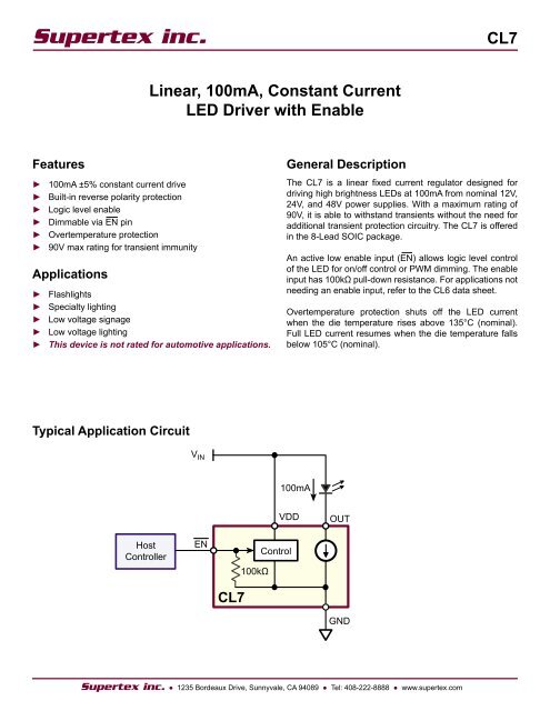
Typical Application Circuit<br />
<strong>Linear</strong>, <strong>100mA</strong>, <strong>Constant</strong> <strong>Current</strong><br />
<strong>LED</strong> <strong>Driver</strong> <strong>with</strong> Enable<br />
Flashlights<br />
Specialty lighting<br />
Low voltage signage<br />
Low voltage lighting<br />
This device is not rated for automotive applications.<br />
Host<br />
Controller<br />
V IN<br />
EN<br />
<strong>CL7</strong><br />
100kΩ<br />
Control<br />
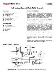
General Description<br />
● 1235 Bordeaux Drive, Sunnyvale, CA 94089 ● Tel: 408-222-8888 ● www.supertex.com<br />
<strong>CL7</strong><br />
The <strong>CL7</strong> is a linear fixed current regulator designed for<br />
driving high brightness <strong>LED</strong>s at <strong>100mA</strong> from nominal 12V,<br />
24V, and 48V power supplies. With a maximum rating of<br />
90V, it is able to <strong>with</strong>stand transients <strong>with</strong>out the need for<br />
additional transient protection circuitry. The <strong>CL7</strong> is offered<br />
in the 8-Lead SOIC package.<br />
An active low enable input (EN) allows logic level control<br />
of the <strong>LED</strong> for on/off control or PWM dimming. The enable<br />
input has 100kΩ pull-down resistance. For applications not<br />
needing an enable input, refer to the CL6 data sheet.<br />
Overtemperature protection shuts off the <strong>LED</strong> current<br />
when the die temperature rises above 135°C (nominal).<br />
Full <strong>LED</strong> current resumes when the die temperature falls<br />
below 105°C (nominal).<br />
<strong>100mA</strong><br />
VDD OUT<br />
GND
Ordering Information<br />
-G indicates package is RoHS compliant (‘Green’)<br />
Absolute Maximum Ratings<br />
Parameter Value<br />
Supply voltage, V DD<br />
Output voltage, V OUT<br />
Enable voltage, V EN<br />
-25V to +100V<br />
-25V to +100V<br />
-0.5V to +6.5V<br />
Operating junction temperature -40°C*<br />
Storage temperature -65°C to +150°C<br />
Absolute Maximum Ratings are those values beyond which damage to the<br />
device may occur. Functional operation under these conditions is not implied.<br />
Continuous operation of the device at the absolute rating level may affect<br />
device reliability. All voltages are referenced to device ground.<br />
Note:<br />
* Maximum junction temperature internally limited.<br />
Note:<br />
1.<br />
2.<br />
Device<br />
8-Lead SOIC (w/Heat Slug)<br />
4.90x3.90mm body<br />
1.70mm height (max)<br />
1.27mm pitch<br />
<strong>CL7</strong> <strong>CL7</strong>SG-G<br />
Thermal Characteristics (Guaranteed by design – not production tested )<br />
Pin Configuration<br />
Pin Designation<br />
Pin Name Description<br />
Sym Parameter Min Typ Max Units Conditions<br />
θJ-A Thermal resistance,<br />
junction to ambient<br />
Power SO-8 - 67 - OC/W 2 Soldered to 2cm exposed copper area<br />
TLIM Overtemperature limit 120 135 150 OC ---<br />
T HYS Overtemperature hysteresis - 30 - O C ---<br />
● 1235 Bordeaux Drive, Sunnyvale, CA 94089 ● Tel: 408-222-8888 ● www.supertex.com<br />
2<br />
<strong>CL7</strong><br />
VDD VDD Supply voltage for the <strong>CL7</strong><br />
OUT Output<br />
Connect the <strong>LED</strong> between this pin and<br />
the supply voltage<br />
GND Ground Circuit common<br />
EN Enable<br />
Active low enable input - this input has<br />
an internal 100kΩ pull-down resistance<br />
Product Marking<br />
YYWW<br />
<strong>CL7</strong><br />
L L L L<br />
Recommended Operating Conditions (all voltages <strong>with</strong> respect to GND pin)<br />
YY = Year Sealed<br />
WW = Week Sealed<br />
L = Lot Number<br />
= “Green” Packaging<br />
8-Lead SOIC w/ Heat Slug (SG)<br />
Sym Parameter Min Typ Max Units Conditions<br />
VDD Supply voltage<br />
Normal<br />
Extended<br />
VOUT Voltage at OUT pin (1) Normal<br />
Extended<br />
6.5<br />
6.5<br />
4.0<br />
4.0<br />
-<br />
-<br />
28<br />
90<br />
28<br />
90<br />
V ---<br />
V ---<br />
T J Junction temperature (2) -40 - 119 o C ---<br />
Continuous operation at high V OUT voltages may result in activation of overtemperature protection. Use appropriate heatsinking.<br />
Maximum junction temperature internally limited.<br />
GND<br />
GND<br />
GND<br />
GND<br />
1<br />
2<br />
3<br />
4<br />
8<br />
7<br />
6<br />
5<br />
VDD<br />
OUT<br />
NC<br />
EN<br />
Heat Slug<br />
8-Lead SOIC w/ Heat Slug (SG)<br />
(top view)<br />
(Heat slug potential is at ground)
Electrical Characteristics<br />
(Over normal recommended operating conditions unless otherwise specified. All voltages <strong>with</strong> respect to GND pin. Production tested @ 25 O C.)<br />
Sym Parameter Min Typ Max Units Conditions<br />
I DD <strong>Current</strong> into VDD pin 3.0 5.0 10 mA ---<br />
I OUT<br />
I OUT(OFF)<br />
<strong>Current</strong> into OUT pin 1<br />
<strong>Current</strong> into OUT pin <strong>with</strong> VDD pin<br />
open or EN=1<br />
95<br />
90<br />
50<br />
100<br />
100<br />
-<br />
105<br />
110<br />
120<br />
● 1235 Bordeaux Drive, Sunnyvale, CA 94089 ● Tel: 408-222-8888 ● www.supertex.com<br />
3<br />
mA<br />
- - 10 µA V DD = open<br />
V EN(ON) Enable voltage, on - - 0.8 V ---<br />
V EN(OFF) Enable voltage, off 2.4 - - V ---<br />
R EN Enable pull-down resistance - 100 - kΩ ---<br />
V OFF<br />
Voltage at VDD to shut off <strong>LED</strong><br />
current<br />
- - 1.0 V I OUT < 10µA<br />
t ON On delay, EN to OUT - 3.0 - µs EN = 0V<br />
t OFF Off delay, EN to OUT - 0.1 - µs EN = 5V<br />
t RISE <strong>Current</strong> rise time, EN to OUT - 4.0 - µs EN = 0V<br />
t FALL <strong>Current</strong> fall time, EN to OUT - 0.3 - µs EN = 5V<br />
Timing<br />
EN<br />
I OUT<br />
I OUT vs Temperature<br />
I OUT (Normalized)<br />
1.05<br />
1.00<br />
0.95<br />
0.90<br />
t ON<br />
t RISE<br />
90%<br />
10%<br />
t OFF<br />
t FALL<br />
0.85<br />
-50 -25 0 25 50 75 100 125<br />
Temperature ( O C)<br />
Normal conditions, 25°C<br />
Normal conditions, full temp 2<br />
Extended conditions<br />
<strong>CL7</strong>
Application Circuits<br />
PWM Dimming 2-Level <strong>LED</strong> Circuit<br />
PWM<br />
signal<br />
EN<br />
V IN<br />
<strong>CL7</strong><br />
100kΩ<br />
Control<br />
VDD OUT<br />
GND<br />
(1-D) • <strong>100mA</strong><br />
D is the portion of time the PWM signal is high.<br />
Control<br />
VDD OUT<br />
GND<br />
● 1235 Bordeaux Drive, Sunnyvale, CA 94089 ● Tel: 408-222-8888 ● www.supertex.com<br />
4<br />
EN<br />
EN = 0: 107.5mA<br />
EN = 1: 7.5mA<br />
<strong>CL7</strong><br />
100kΩ<br />
Minimum V IN is increased by <strong>LED</strong> drop.<br />
V IN<br />
<strong>CL7</strong>
8-Lead SOIC (Narrow Body w/Heat Slug) Package Outline (SG)<br />
4.90x3.90mm body, 1.70mm height (max), 1.27mm pitch<br />
Note 1<br />
(Index Area<br />
D/2 x E1/2)<br />
A A2<br />
A1<br />
Symbol A A1 A2 b D D1 E E1 E2 e h L L1 L2 θ θ1<br />
Dimension<br />
(mm)<br />
(The package drawing(s) in this data sheet may not reflect the most current specifications. For the latest package outline<br />
information go to http://www.supertex.com/packaging.html.)<br />
<strong>Supertex</strong> inc. does not recommend the use of its products in life support applications, and will not knowingly sell them for use in such applications unless it receives an<br />
adequate “product liability indemnification insurance agreement.” <strong>Supertex</strong> inc. does not assume responsibility for use of devices described, and limits its liability to the<br />
replacement of the devices determined defective due to workmanship. No responsibility is assumed for possible omissions and inaccuracies. Circuitry and specifications<br />
are subject to change <strong>with</strong>out notice. For the latest product specifications refer to the <strong>Supertex</strong> inc. website: http//www.supertex.com.<br />
©2008 All rights reserved. Unauthorized use or reproduction is prohibited.<br />
Doc.# DSFP-<strong>CL7</strong><br />
A102908<br />
8<br />
1<br />
D<br />
Top View<br />
e b<br />
E1 E<br />
Seating<br />
Plane<br />
A<br />
A<br />
Side View View A - A View B<br />
5<br />
View B<br />
<strong>CL7</strong><br />
MIN 1.25* 0.00 1.25 0.31 4.80* 3.30 † 5.80* 3.80* 2.29 † 0.25 0.40<br />
0<br />
1.27<br />
BSC<br />
1.04<br />
REF<br />
0.25<br />
BSC<br />
O 5O NOM - - - - 4.90 - 6.00 3.90 - - - - -<br />
MAX 1.70 0.15 1.55* 0.51 5.00* 3.81 † 6.20* 4.00* 2.79 † 0.50 1.27 8 O 15 O<br />
JEDEC Registration MS-012, Variation BA, Issue E, Sept. 2005.<br />
* This dimension is not specified in the original JEDEC drawing. The value listed is for reference only.<br />
† This dimension is a non-JEDEC dimension.<br />
Drawings not to scale.<br />
<strong>Supertex</strong> Doc. #: DSPD-8SOSG, Version C090408.<br />
h<br />
h<br />
D1<br />
Bottom View<br />
Note 1<br />
8<br />
1<br />
Exposed<br />
Thermal<br />
Pad Zone<br />
E2<br />
θ1<br />
L<br />
L1<br />
L2<br />
Gauge<br />
Plane<br />
Seating<br />
Plane<br />
Notes:<br />
1.<br />
If optional chamfer feature is not present, a Pin 1 identifier must be located in the index area indicated. The Pin 1 identifier can be: a molded mark/<br />
identifier; an embedded metal marker; or a printed indicator.<br />
1235 Bordeaux Drive, Sunnyvale, CA 94089<br />
Tel: 408-222-8888<br />
www.supertex.com<br />
θ