SiO2 etching with ZEP520A resist mask - Nanolithography
SiO2 etching with ZEP520A resist mask - Nanolithography
SiO2 etching with ZEP520A resist mask - Nanolithography

You also want an ePaper? Increase the reach of your titles
YUMPU automatically turns print PDFs into web optimized ePapers that Google loves.
Si <strong>etching</strong><br />
<strong>with</strong> <strong>ZEP520A</strong> <strong>resist</strong><br />
and oxide hard <strong>mask</strong><br />
Devin Brown<br />
2/04/09
Summary<br />
• <strong>ZEP520A</strong> typically has a 1:1 dry plasma etch<br />
selectivity relative to Si and <strong>SiO2</strong><br />
• required lateral pattern dimensions usually<br />
restrict <strong>ZEP520A</strong> thickness to less than 600nm<br />
• if more than 600nm of Si or <strong>SiO2</strong> is desired to be<br />
etched, then 600nm of ZEP20A will be<br />
insufficient<br />
• this summary shows how an <strong>SiO2</strong> "hard <strong>mask</strong>"<br />
can be used to etch Silicon to depths beyond<br />
what would be possible <strong>with</strong> <strong>ZEP520A</strong> alone
<strong>ZEP520A</strong> <strong>resist</strong><br />
PECVD oxide<br />
silicon substrate<br />
<strong>ZEP520A</strong> <strong>resist</strong><br />
PECVD oxide<br />
1. <strong>resist</strong> coat<br />
2. EBL expose/develop<br />
silicon substrate<br />
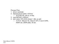
Process Flow<br />
3. <strong>SiO2</strong> hard <strong>mask</strong> etch<br />
<strong>ZEP520A</strong> <strong>resist</strong><br />
PECVD oxide<br />
silicon substrate<br />
PECVD oxide<br />
silicon substrate<br />
4. Si etch
Process Flow<br />
• PECVD oxide dep<br />
• Resist Coat<br />
– <strong>ZEP520A</strong><br />
• EBL exposure<br />
– 100kV, 2nA<br />
• Resist Develop<br />
– 2min immersion n-Amyl Acetate, 30sec immersion IPA rinse<br />
• <strong>SiO2</strong> etch<br />
– Plasma Therm ICP<br />
– 5mTorr, 25sccm C4F6, 15sccm CF4, 4sccm Ar, 4sccm O2, RF1 =<br />
400W, RF2 = 400W<br />
• Si etch<br />
– STS SOE ICP<br />
– 5mTorr, 20sccm Cl2, 5sccm Ar, coil = 600W, plate = 50W
Post expose/develop
<strong>ZEP520A</strong><br />
Si substrate<br />
2um line post expose/develop<br />
PECVD <strong>SiO2</strong>
<strong>ZEP520A</strong><br />
PECVD <strong>SiO2</strong><br />
0.5um line post expose/develop<br />
Si substrate
100nm line post expose/develop<br />
<strong>ZEP520A</strong><br />
PECVD <strong>SiO2</strong><br />
Si substrate
Post partial <strong>SiO2</strong> etch
<strong>ZEP520A</strong><br />
PECVD <strong>SiO2</strong><br />
2um line post 30sec <strong>SiO2</strong> etch<br />
Si substrate
0.5um line post 30sec <strong>SiO2</strong> etch<br />
<strong>ZEP520A</strong><br />
PECVD <strong>SiO2</strong><br />
Si substrate
100nm line post 30sec <strong>SiO2</strong> etch<br />
<strong>ZEP520A</strong><br />
PECVD <strong>SiO2</strong><br />
Si substrate
Post expose/develop and before etch<br />
parameter data<br />
PECVD oxide thickness mean = 293nm, st dev = 14nm, N = 8<br />
<strong>ZEP520A</strong> <strong>resist</strong> thickness mean = 389nm, st dev = 4nm, N = 3<br />
After 30sec of <strong>SiO2</strong> etch<br />
parameter data<br />
PECVD oxide thickness<br />
etched<br />
PECVD oxide etch rate 3.9nm/s<br />
<strong>ZEP520A</strong> <strong>resist</strong> thickness<br />
remaining<br />
ZEP520 <strong>resist</strong> etch rate 3.4nm/s<br />
selectivity<br />
PECVD oxide : ZEP520<br />
mean = 116nm, st dev = 16nm, N = 5<br />
mean = 286nm, st dev = 21nm, N = 5<br />
1.1 : 1<br />
time required to fully etch 293nm of PECVD oxide + 10% overetch = 83sec<br />
(slides that follow show <strong>SiO2</strong> fully etched at 83sec)
Post full <strong>SiO2</strong> etch
PECVD <strong>SiO2</strong><br />
2um line post 83sec <strong>SiO2</strong> etch<br />
<strong>ZEP520A</strong><br />
Si substrate
0.5um line post 83sec <strong>SiO2</strong> etch<br />
<strong>ZEP520A</strong><br />
PECVD <strong>SiO2</strong><br />
Si substrate
100nm line post 83sec <strong>SiO2</strong> etch<br />
<strong>ZEP520A</strong><br />
PECVD <strong>SiO2</strong><br />
Si substrate
Post partial Si etch<br />
(<strong>resist</strong> was not removed)
2um line post 120sec Si etch
0.5um line post 120sec Si etch
100nm line post 120sec Si etch
parameter data<br />
After 120sec of Si etch<br />
Resist was not removed after <strong>SiO2</strong> etch and prior to Si etch, because it can help provide<br />
some small extra buffer for Si <strong>etching</strong>. The etch rate of <strong>resist</strong> <strong>with</strong> the DEVIN1.SET<br />
recipe is known to be ~4.6nm/sec. Prior to this etch, there was 139nm of <strong>resist</strong> still<br />
remaining. So, after 30sec, the 139nm of <strong>resist</strong> will be gone, and then the oxide <strong>mask</strong><br />
layer will be exposed. The data in the table summarizes the etch parameters.<br />
PECVD oxide thickness etched mean = 41nm, st dev = 6nm, N = 8<br />
PECVD oxide etch rate 0.45nm/s<br />
silicon etched mean = 599nm<br />
sigma = 7nm<br />
N = 2<br />
2um line 500nm line 100nm line<br />
mean = 625nm<br />
sigma = 5nm<br />
N = 2<br />
mean = 493nm<br />
sigma = 19nm<br />
N = 3<br />
silicon etch rate 5.0nm/s 5.2nm/s 4.1nm/s<br />
selectivity to oxide 11.1 11.6 9.1<br />
note: sample size is small, don’t expect 2um line to etch more slowly than 500nm line