Code for Bank-Switching with the 653X-Series - Maxim
Code for Bank-Switching with the 653X-Series - Maxim
Code for Bank-Switching with the 653X-Series - Maxim
You also want an ePaper? Increase the reach of your titles
YUMPU automatically turns print PDFs into web optimized ePapers that Google loves.
A <strong>Maxim</strong> Integrated Products Brand<br />
71M<strong>653X</strong><br />
Energy Meter IC<br />
APPLICATION NOTE<br />
AN_<strong>653X</strong>_006 OCTOBER 2008<br />
<strong>Code</strong> <strong>for</strong> <strong>Bank</strong>-<strong>Switching</strong> <strong>with</strong> <strong>the</strong> <strong>653X</strong>-<strong>Series</strong><br />
This document describes how to use banked code <strong>with</strong> a 71M6531. Similar principles apply <strong>for</strong> <strong>the</strong> 71M6533 and<br />
71M6534.<br />
Introduction<br />
The 80515 microcontroller contained in <strong>the</strong> TERIDIAN 71M<strong>653X</strong> Energy Meter chips can only address 64 KB of<br />
code. This Application Note explains how to design firmware <strong>with</strong> more than 64 KB of code <strong>for</strong> <strong>the</strong> 71M<strong>653X</strong> Energy<br />
Meter chips.<br />
Theory of Operation<br />
The Hardware<br />
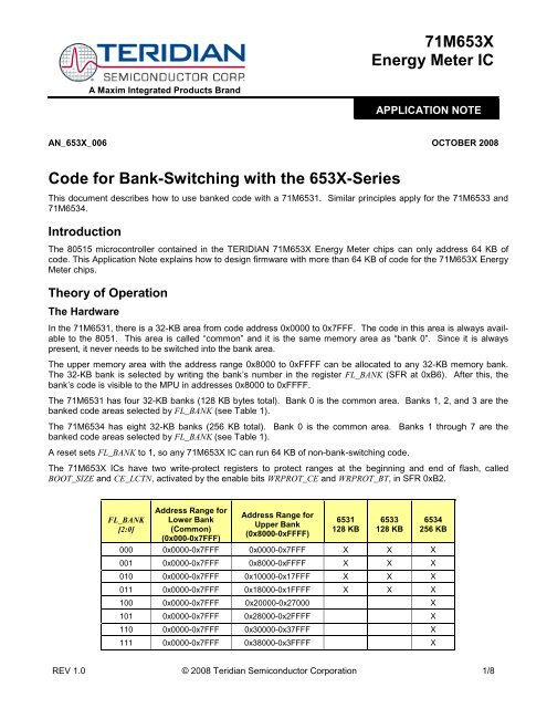
In <strong>the</strong> 71M6531, <strong>the</strong>re is a 32-KB area from code address 0x0000 to 0x7FFF. The code in this area is always available<br />
to <strong>the</strong> 8051. This area is called “common” and it is <strong>the</strong> same memory area as “bank 0”. Since it is always<br />
present, it never needs to be switched into <strong>the</strong> bank area.<br />
The upper memory area <strong>with</strong> <strong>the</strong> address range 0x8000 to 0xFFFF can be allocated to any 32-KB memory bank.<br />
The 32-KB bank is selected by writing <strong>the</strong> bank’s number in <strong>the</strong> register FL_BANK (SFR at 0xB6). After this, <strong>the</strong><br />
bank’s code is visible to <strong>the</strong> MPU in addresses 0x8000 to 0xFFFF.<br />
The 71M6531 has four 32-KB banks (128 KB bytes total). <strong>Bank</strong> 0 is <strong>the</strong> common area. <strong>Bank</strong>s 1, 2, and 3 are <strong>the</strong><br />
banked code areas selected by FL_BANK (see Table 1).<br />
The 71M6534 has eight 32-KB banks (256 KB total). <strong>Bank</strong> 0 is <strong>the</strong> common area. <strong>Bank</strong>s 1 through 7 are <strong>the</strong><br />
banked code areas selected by FL_BANK (see Table 1).<br />
A reset sets FL_BANK to 1, so any 71M<strong>653X</strong> IC can run 64 KB of non-bank-switching code.<br />
The 71M<strong>653X</strong> ICs have two write-protect registers to protect ranges at <strong>the</strong> beginning and end of flash, called<br />
BOOT_SIZE and CE_LCTN, activated by <strong>the</strong> enable bits WRPROT_CE and WRPROT_BT, in SFR 0xB2.<br />
FL_BANK<br />
[2:0]<br />
Address Range <strong>for</strong><br />
Lower <strong>Bank</strong><br />
(Common)<br />
(0x000-0x7FFF)<br />
Address Range <strong>for</strong><br />
Upper <strong>Bank</strong><br />
(0x8000-0xFFFF)<br />
6531<br />
128 KB<br />
6533<br />
128 KB<br />
6534<br />
256 KB<br />
000 0x0000-0x7FFF 0x0000-0x7FFF X X X<br />
001 0x0000-0x7FFF 0x8000-0xFFFF X X X<br />
010 0x0000-0x7FFF 0x10000-0x17FFF X X X<br />
011 0x0000-0x7FFF 0x18000-0x1FFFF X X X<br />
100 0x0000-0x7FFF 0x20000-0x27000 X<br />
101 0x0000-0x7FFF 0x28000-0x2FFFF X<br />
110 0x0000-0x7FFF 0x30000-0x37FFF X<br />
111 0x0000-0x7FFF 0x38000-0x3FFFF X<br />
REV 1.0 © 2008 Teridian Semiconductor Corporation 1/8
Table 1<br />
<strong>Code</strong> <strong>for</strong> <strong>Bank</strong>-<strong>Switching</strong> <strong>with</strong> <strong>the</strong> <strong>653X</strong>-<strong>Series</strong><br />
The 71M<strong>653X</strong> ICs’ flash memory are very similar to <strong>the</strong> ROM arrangement in Keil’s example “<strong>Bank</strong>ing <strong>with</strong> Common<br />
Area” of chapter 9 (linker) of Keil’s “Macro assembler and Utilities” manual.<br />
The Software<br />
TERIDIAN’s demonstration code uses <strong>the</strong> Keil compiler’s standard bank switching system (www.keil.com).<br />
<strong>Bank</strong>-switching is completely supported by Keil, a major compiler vendor <strong>for</strong> generic 8051 processors and cores,<br />
and Signum, <strong>the</strong> emulator vendor. <strong>Code</strong> can be ported from non-banked projects, and full symbolic banked debugging<br />
is available.<br />
Keil’s scheme puts a “page table” in common memory. <strong>Code</strong> calls an entry in <strong>the</strong> page table. The entry is a bit of<br />
code that switches to <strong>the</strong> subroutine’s bank, and jumps to <strong>the</strong> subroutine in <strong>the</strong> bank.<br />
Keil’s linker automatically produces <strong>the</strong> page table. In TERIDIAN’s Demo <strong>Code</strong>, <strong>the</strong> size of this table is less than 1<br />
KB.<br />
<strong>Code</strong> using <strong>the</strong> page table is slower than native 16-bit code, because it has to set <strong>the</strong> page register.<br />
Interrupts must start in <strong>the</strong> common (non-banked) area, because <strong>the</strong> bank register could have any value.<br />
Calls via function pointers (e.g. “callback routines”) are supported, but need to be made global, and mapped to <strong>the</strong>ir<br />
caller <strong>with</strong> <strong>the</strong> linker’s overlay functions. Keil’s linker often omits callback routines from <strong>the</strong> page table when it optimizes<br />
<strong>the</strong> page table, and this causes incorrect operation.<br />
Constant values have to be accessed from <strong>the</strong> same bank, or common code. When accessed from common code<br />
<strong>the</strong> bank has to be switched manually <strong>with</strong> switchbank(), a subroutine in <strong>the</strong> bank logic.<br />
Design and Coding<br />
Software Versions<br />
The development software used <strong>with</strong> <strong>the</strong>se examples was Keil C version 8.03, <strong>with</strong> <strong>the</strong> BL51 linker (<strong>the</strong> Lx51 linker<br />
is actually easier to use, but not shown). The Signum emulator software used was version 3.11.04.<br />
Setup of <strong>the</strong> Compiler Project<br />
This dialogue is <strong>for</strong> <strong>the</strong> project options of a 71M6531, which has four banks (see Figure 1).<br />
Figure 1: Project Setup<br />
REV 1.0 © 2008 Teridian Semiconductor Corporation 2/8
<strong>Code</strong> <strong>for</strong> <strong>Bank</strong>-<strong>Switching</strong> <strong>with</strong> <strong>the</strong> <strong>653X</strong>-<strong>Series</strong><br />
When opening individual files by right-clicking on <strong>the</strong> file names (after opening <strong>the</strong> group folders listed under “Target”),<br />
file options can be edited. These options can be set to assign code to certain pages (as shown in Figure 2:<br />
Assigning <strong>Bank</strong> Numbers to <strong>Code</strong><br />
Startup <strong>Code</strong><br />
Figure 2: Assigning <strong>Bank</strong> Numbers to <strong>Code</strong><br />
TERIDIAN provides special start-up code on <strong>the</strong> CD-ROMs shipped <strong>with</strong> <strong>the</strong> 71M<strong>653X</strong> Demo Kits. The code can be<br />
found at Util\startup_30_banked.a51. This file sets up <strong>the</strong> bank-switching logic. It must be included in <strong>the</strong> build.<br />
Any o<strong>the</strong>r startup.a51 file must be removed.<br />
<strong>Bank</strong>-<strong>Switching</strong> <strong>Code</strong><br />
TERIDIAN has already ported Keil’s bank-switching code, Util\L51_bank.a51. TERIDIAN’s version of this file should<br />
be included in <strong>the</strong> build. TERIDIAN has already selected <strong>the</strong> fastest standard bank-switching method as <strong>the</strong> default.<br />
During per<strong>for</strong>mance testing, TERIDIAN made a good-faith attempt to port <strong>the</strong> o<strong>the</strong>r bank-switching methods in this<br />
code, including features needed by Keil’s advanced Lx51 linker. However <strong>the</strong>se versions are not extensively tested.<br />
Page Table<br />
Keil’s linkers produce <strong>the</strong> page table automatically, once paging is selected in <strong>the</strong> Microvision options->target dialogue.<br />
The Keil tools usually places <strong>the</strong> page table at an address of 0x100 in <strong>the</strong> common bank. It is visible in <strong>the</strong><br />
linker .m51 file. To see how it works, one can use <strong>the</strong> emulator to single-step through at a banked function call at<br />
<strong>the</strong> assembly language level.<br />
To call a paged subroutine, Keil’s linker arranges to call one of <strong>the</strong> entries of <strong>the</strong> page table. The page table consists<br />
of one entry per subroutine. Each entry is a small piece of code that loads <strong>the</strong> address of <strong>the</strong> banked subroutine<br />
into <strong>the</strong> 8051 register DPTR, and <strong>the</strong>n jumps to paging code. The paging code sets <strong>the</strong> bank register FL_BANK,<br />
and <strong>the</strong>n jumps to <strong>the</strong> banked code’s address contained in <strong>the</strong> DPTR.<br />
REV 1.0 © 2008 Teridian Semiconductor Corporation 3/8
<strong>Code</strong> <strong>for</strong> <strong>Bank</strong>-<strong>Switching</strong> <strong>with</strong> <strong>the</strong> <strong>653X</strong>-<strong>Series</strong><br />
Keil’s linkers minimize <strong>the</strong> size of <strong>the</strong> page table. A subroutine has an entry in <strong>the</strong> page table only if:<br />
1. The subroutine is in a bank, and<br />
2. The subroutine is called from outside its bank.<br />
Most problems <strong>with</strong> banking code occur because <strong>the</strong> linker omits a function from <strong>the</strong> page table. The result is that<br />
<strong>the</strong> call to a function in a different bank goes to code in <strong>the</strong> current bank, causing unexpected code in <strong>the</strong> current<br />
bank to be executed.<br />
One major cause of this is a callback subroutine called via a function pointer. Ano<strong>the</strong>r is an interrupt defined in<br />
banked assembly language file (<strong>for</strong>tunately, Keil detects and flags banked interrupts in C code).<br />
To solve problems stemming from callback routines, all subroutines called from o<strong>the</strong>r banks should be made global,<br />
so that <strong>the</strong> linker can use <strong>the</strong>ir data.<br />
Next, overlay commands should be used to in<strong>for</strong>m <strong>the</strong> Keil linker that a banked function is called from a caller in a<br />
different bank. This <strong>for</strong>ces <strong>the</strong> linker to put <strong>the</strong> callee function into <strong>the</strong> page table. To use <strong>the</strong> overlay command in<br />
<strong>the</strong> linker, see <strong>the</strong> discussion of “overlay” in <strong>the</strong> Keil linker’s documentation. Here is an example of <strong>the</strong> overlay<br />
commands from <strong>the</strong> Demo <strong>Code</strong>. These commands map <strong>the</strong> callback routines that are called from <strong>the</strong> software timer,<br />
and hardware timer interrupt 0.<br />
Figure 3: Linker Dialog Box<br />
However, if <strong>the</strong>re should be o<strong>the</strong>r problems, <strong>the</strong>re is a way to isolate <strong>the</strong>m:<br />
1. Remove code from <strong>the</strong> project until all code fits in common and bank 1.<br />
2. Move modules individually each to a bank until <strong>the</strong> problem occurs.<br />
3. At some point, <strong>the</strong> problem is likely to show up as an unexpected reset. What is happening here is that <strong>the</strong><br />
call to code in bank 1 is probably going to uninitialized code memory in ano<strong>the</strong>r bank. It will execute until<br />
<strong>the</strong> program counter wraps around to zero and begins executing <strong>the</strong> reset vector.<br />
4. Place a break point near <strong>the</strong> end of <strong>the</strong> o<strong>the</strong>r bank, to catch <strong>the</strong> erroneous execution.<br />
5. After trapping <strong>the</strong> error, set <strong>the</strong> program counter to <strong>the</strong> address of a RET instruction, and single-step. The<br />
code will return to <strong>the</strong> code that called <strong>the</strong> wrong bank.<br />
6. Fix <strong>the</strong> calling routine, and all similar problems!<br />
REV 1.0 © 2008 Teridian Semiconductor Corporation 4/8
Generating a Hex File<br />
<strong>Code</strong> <strong>for</strong> <strong>Bank</strong>-<strong>Switching</strong> <strong>with</strong> <strong>the</strong> <strong>653X</strong>-<strong>Series</strong><br />
The BL51 linker and its associated hex converter produce a separate Intel hex file <strong>for</strong> each bank. These files end<br />
<strong>with</strong> names such as .H01 <strong>for</strong> bank 1, .H02 <strong>for</strong> bank 2, etc. The emulator and <strong>the</strong> production programmer expect a<br />
single Intel 386 hex file <strong>with</strong> a .HEX ending.<br />
TERIDIAN’s demo CD ROM has a utility called bank_merge.exe. It runs in a DOS command window and merges<br />
<strong>the</strong> bank files from Keil’s hex converter into one Intel-386 hex file. This can be placed in <strong>the</strong> build automatically.<br />
Running bank_merge in <strong>the</strong> build uses a feature in Keil uVision3. Keil’s uVision3 integrated development environment<br />
can run DOS command-line programs after it finishes building software. Right-click <strong>the</strong> project name in <strong>the</strong><br />
project work-space window to view <strong>the</strong> project’s options. click <strong>the</strong> output tab. Check <strong>the</strong> box, “Run user program<br />
#1”, and fill <strong>the</strong> associated line <strong>with</strong> <strong>the</strong> bank merge command-line (see Figure 4). For example:<br />
ce\bank_merge 128 6531_demo_2sc.abs 6531_demo_2sc.hex<br />
“128” is <strong>the</strong> size of <strong>the</strong> 6531’s flash in 1-KB increments. A 6534 should have “256.” The first file name<br />
“6531_demo_2sc.abs” tells which name of <strong>the</strong> .H0x files made by <strong>the</strong> Keil utilities. The file-type suffix ‘.abs’ is ignored.<br />
The second name, “6531_demo_2sc.hex”, is <strong>the</strong> output hex file’s name.<br />
Figure 4: Output Options Dialog Box<br />
Ano<strong>the</strong>r manual solution is to erase <strong>the</strong> flash, load <strong>the</strong> .abs file to an emulator, and <strong>the</strong>n use <strong>the</strong> file->save range: All<br />
menu selection to save a copy of flash as an Intel hex file.<br />
When using Keil’s Lx51 advanced linker, <strong>the</strong> output dialog contains a pull-down list of hex <strong>for</strong>mats. Select <strong>the</strong> “i386”<br />
hex file option.<br />
The emulator’s verification option is a convenient way to verify that <strong>the</strong> .abs and .hex file have <strong>the</strong> same content. To<br />
use it, invoke <strong>the</strong> menu File->Load, <strong>the</strong>n check <strong>the</strong> verify box, but not <strong>the</strong> load box.<br />
REV 1.0 © 2008 Teridian Semiconductor Corporation 5/8
Interrupts<br />
<strong>Code</strong> <strong>for</strong> <strong>Bank</strong>-<strong>Switching</strong> <strong>with</strong> <strong>the</strong> <strong>653X</strong>-<strong>Series</strong><br />
The interrupts must start in <strong>the</strong> common code. TERIDIAN Demo <strong>Code</strong> starts most interrupts from a “trampoline”<br />
routine that saves and restores <strong>the</strong> bank register. The Demo <strong>Code</strong>’s trampoline routines are in Meter\io653x.c, <strong>with</strong><br />
<strong>the</strong> stub interrupts and decoded interrupts. An example of a trampoline is shown below. It is a serial interrupt code<br />
from Meter\io653x.c, used to service UART0:<br />
#pragma save<br />
#pragma REGISTERBANK (ES0_BANK)<br />
void es0_trampoline (void) small reentrant interrupt ES0_IV using ES0_BANK<br />
{<br />
uint8_t my_fl_bank = FL_BANK; // save <strong>the</strong> bank register<br />
FL_BANK = BANK_DEFAULT; // BANK_DEFAULT is 1<br />
es0_isr();<br />
FL_BANK = my_fl_bank; // restore <strong>the</strong> bank register<br />
}<br />
#pragma restore<br />
This is clumsy and slow. Why do this?<br />
A trampoline lets most interrupt code be in bank-switched code space <strong>with</strong> o<strong>the</strong>r code from <strong>the</strong> same file. This<br />
makes <strong>the</strong> code easier to read. It also leaves more space in common memory, and permits a larger system to exist.<br />
The penalty is a delay of a few tens of microseconds per interrupt.<br />
Very frequent interrupts should not use trampoline routines. In TERIDIAN’s Demo <strong>Code</strong>, <strong>the</strong> CE code, Meter\ce.c<br />
has an interrupt that runs every 396 microseconds (ce_busy_isr()). ce.c is placed in <strong>the</strong> common area, and<br />
ce_busy’s trampoline is disabled (in Meter\io653x.c).<br />
If an interrupt calls code in a bank, as shown above, it must save and restore <strong>the</strong> bank-switching register, FL_BANK.<br />
Keil’s Lx51 advanced linker has an option to automatically save and restore <strong>the</strong> bank register in an interrupt. TERI-<br />
DIAN’s L51_bank.a51 code provides <strong>the</strong> necessary symbols.<br />
Calls via Function Pointers<br />
In a bank-switching system, functions placed in function pointers cannot have <strong>the</strong> word “static” in front of <strong>the</strong>ir definition;<br />
<strong>the</strong>y must be global.<br />
Additionally, <strong>the</strong> linker must be in<strong>for</strong>med of <strong>the</strong> actual caller of <strong>the</strong> function in <strong>the</strong> function pointers. For example, in<br />
<strong>the</strong> TERIDIAN Demo <strong>Code</strong>, <strong>the</strong> software timer module (Util\stm.c) calls many routines. There is also an interrupt <strong>for</strong><br />
hardware timer 1 that calls <strong>the</strong> software timer’s interrupt code. This linker dialogue tells <strong>the</strong> linker <strong>the</strong> true relationship.<br />
The command to <strong>the</strong> linker is “caller ! callee” or “caller ! (callee_1, callee_2, …)” (See <strong>the</strong> linker command<br />
Figure 3).<br />
Why do this? If a function pointer points at a function’s entry in <strong>the</strong> page table, <strong>the</strong> function pointer can be executed<br />
from any bank, at any time. So, in <strong>the</strong>ory, function pointers are supported via <strong>the</strong> page table.<br />
In practice, <strong>the</strong> Keil linker tries to save space in <strong>the</strong> page table. To do this, it only puts global functions into <strong>the</strong> page<br />
table if <strong>the</strong>y are in a bank area and are called from outside <strong>the</strong> bank. Often, function pointers are used <strong>for</strong> callback<br />
routines. In <strong>the</strong>se cases, <strong>the</strong> linker often does not detect <strong>the</strong> true caller and so cannot detect <strong>the</strong> cross-bank function<br />
call. Then, it places a banked address into <strong>the</strong> code that sets <strong>the</strong> function pointer. If this is executed from<br />
ano<strong>the</strong>r bank, <strong>the</strong> code jumps to code in <strong>the</strong> current, wrong bank!<br />
Using overlay commands in<strong>for</strong>ms <strong>the</strong> linker of <strong>the</strong> actual caller, so it can detect cross-bank calls.<br />
To increase reliability, <strong>the</strong> Demo <strong>Code</strong> that sets a function pointer also checks to make sure that <strong>the</strong> pointer is in<br />
common memory ra<strong>the</strong>r than a bank. A sample of <strong>the</strong> code is shown below:<br />
if (((uint16_t)fn_ptr) > 0x7FFF) // only accept functions in common<br />
{<br />
main_software_error (); // report a software error at a central breakpoint.<br />
return NULL; // indicate a failure to <strong>the</strong> caller<br />
}<br />
REV 1.0 © 2008 Teridian Semiconductor Corporation 6/8
Putting Constants in <strong>Bank</strong>s<br />
<strong>Code</strong> <strong>for</strong> <strong>Bank</strong>-<strong>Switching</strong> <strong>with</strong> <strong>the</strong> <strong>653X</strong>-<strong>Series</strong><br />
Space in <strong>the</strong> common code area can be precious in a large project. It often helps to put a few large tables in a different<br />
code bank. The TERIDIAN Demo <strong>Code</strong>, <strong>for</strong> example, places <strong>the</strong> help text, CE code and <strong>the</strong> CE’s data initialization<br />
table into banked flash.<br />
In order <strong>for</strong> this to work, every reference to <strong>the</strong> data must be from <strong>the</strong> same bank or from common.<br />
In <strong>the</strong> Demo <strong>Code</strong>, <strong>the</strong> largest set of constant tables is <strong>the</strong> help text. The help text (CLI\Help.c) is in <strong>the</strong> same bank<br />
as <strong>the</strong> printing routines, which copy <strong>the</strong> text into RAM <strong>for</strong> use by <strong>the</strong> serial interrupts (see CLI\io.c). Since <strong>the</strong> help<br />
text is in <strong>the</strong> same bank as <strong>the</strong> accessing routines, no o<strong>the</strong>r special coding is needed.<br />
In <strong>the</strong> TERIDIAN Demo <strong>Code</strong>, <strong>the</strong> CE code is referenced from <strong>the</strong> Meter\ce.c. ce.c could not be placed in <strong>the</strong> last<br />
bank <strong>with</strong> <strong>the</strong> tables because it also has a very fast interrupt, ce_busy_isr(), so ce.c was placed in common. Also,<br />
<strong>the</strong> CE code is in <strong>the</strong> last bank, so <strong>the</strong> code in ce.c had to explicitly switch it in to read it.<br />
Designers must be careful that any code in common is smaller than <strong>the</strong> data table! Some systems may need a library<br />
routine in common to copy part of <strong>the</strong> banked data to RAM <strong>for</strong> use by banked code. The TERIDIAN Demo<br />
<strong>Code</strong> does not use this technique because <strong>for</strong>tunately, <strong>the</strong> help system fits in <strong>the</strong> same bank as <strong>the</strong> serial output<br />
routines.<br />
Next, <strong>the</strong> data should be located in <strong>the</strong> desired bank, using compiler and linker’s BANK commands. (See <strong>the</strong> compiler<br />
and linker command in Figure 2 and Figure 3).<br />
The code accessing <strong>the</strong> banked data should include Util\bank.h, which defines switchbank() to access banked<br />
data.<br />
In <strong>the</strong> code that accesses <strong>the</strong> data, <strong>the</strong> bank must be switched in. For example, when <strong>the</strong> Demo <strong>Code</strong> copies <strong>the</strong><br />
starting data <strong>for</strong> <strong>the</strong> CE (ce_init() in Meter\ce.c), it executes <strong>the</strong> following code:<br />
switchbank (BANK_CE);<br />
memcpy_cer (<br />
(int32x_t *)CE_DATA_BASE,<br />
(int32r_t *)&CeData[0],<br />
(uint8_t)(0xff & NumCeData)<br />
);<br />
switchbank () sets <strong>the</strong> bank register <strong>with</strong>out side effects <strong>for</strong> o<strong>the</strong>r bank switching. It is defined in Util\bank.h.<br />
BANK_CE is <strong>the</strong> bank number containing <strong>the</strong> CE initialization table (in Main_6531\options.h or<br />
Main_6534\Options.h).<br />
memcpy_cer () copies 32-bit words from code to CE memory. CE_DATA_BASE is <strong>the</strong> start of CE memory,<br />
0x0000 in XDATA in 71M653x ICs. CeData[] is <strong>the</strong> array of 32-bit integers containing <strong>the</strong> CE’s default data. Num-<br />
CeData is <strong>the</strong> count of data words in <strong>the</strong> table, a constant value that precedes <strong>the</strong> CE default data table.<br />
Write-Protecting Flash Memory<br />
In addition to safety interlocks in software that prevent accidental write operations to flash, <strong>the</strong> 71M653x ICs also<br />
have a write-protection mechanism implemented in hardware. Some systems might permit code or customization<br />
tables to be downloaded to flash memory, and designers might wish to assure that this process cannot corrupt o<strong>the</strong>r<br />
code or data.<br />
To protect flash starting at address 0x00000, write <strong>the</strong> number of 1,024-byte blocks into BOOT_SIZE (at XDATA<br />
0x20A7), and set WRPROT_BT (bit 5 of SFR 0xB2). Since this range covers <strong>the</strong> code’s interrupt vectors, it is perfect<br />
<strong>for</strong> protecting a boot loader (i.e. code that can load o<strong>the</strong>r code into <strong>the</strong> system). It is also <strong>the</strong> logical choice <strong>for</strong> general-purpose<br />
write-protection.<br />
To protect flash near <strong>the</strong> end of memory, place <strong>the</strong> CE’s data area at that point (and set CE_LCTN, XDATA 0x20A8),<br />
and set <strong>the</strong> WRPROT_CE (bit 4 of SFR 0xB2). This protects not only <strong>the</strong> CE code, but also all flash memory after it.<br />
This is excellent <strong>for</strong> protecting <strong>the</strong> CE code and calibration tables stored in flash. The Demo <strong>Code</strong> uses this method<br />
to protect <strong>the</strong> CE code and its default initialization table.<br />
REV 1.0 © 2008 Teridian Semiconductor Corporation 7/8
Revision History<br />
Revision Date Description<br />
Rev. 1.0 10/16/2008 First publication.<br />
<strong>Code</strong> <strong>for</strong> <strong>Bank</strong>-<strong>Switching</strong> <strong>with</strong> <strong>the</strong> <strong>653X</strong>-<strong>Series</strong><br />
<strong>Maxim</strong> cannot assume responsibility <strong>for</strong> use of any circuitry o<strong>the</strong>r than circuitry entirely embodied in a <strong>Maxim</strong> product. No circuit patent licenses<br />
are implied. <strong>Maxim</strong> reserves <strong>the</strong> right to change <strong>the</strong> circuitry and specifications <strong>with</strong>out notice at any time.<br />
<strong>Maxim</strong> Integrated Products, 120 San Gabriel Drive, Sunnyvale, CA 94086 408- 737- 7600<br />
© 2010 <strong>Maxim</strong> Integrated Products <strong>Maxim</strong> is a registered trademark of <strong>Maxim</strong> Integrated Products.


