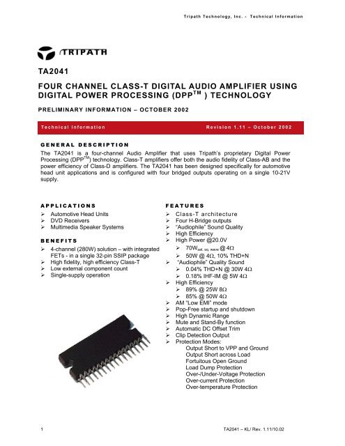
ta2041 four channel class-t digital audio amplifier using digital ...
ta2041 four channel class-t digital audio amplifier using digital ...
ta2041 four channel class-t digital audio amplifier using digital ...

You also want an ePaper? Increase the reach of your titles
YUMPU automatically turns print PDFs into web optimized ePapers that Google loves.
TA2041<br />
Tripath Technology, Inc. - Technical Information<br />
FOUR CHANNEL CLASS-T DIGITAL AUDIO AMPLIFIER USING<br />
DIGITAL POWER PROCESSING (DPP TM ) TECHNOLOGY<br />
PRELIMINARY INFORMATION – OCTOBER 2002<br />
Technical Information Revision 1.11 – October 2002<br />
GENERAL DESCRIPTION<br />
The TA2041 is a <strong>four</strong>-<strong>channel</strong> Audio Amplifier that uses Tripath’s proprietary Digital Power<br />
Processing (DPP TM ) technology. Class-T <strong>amplifier</strong>s offer both the <strong>audio</strong> fidelity of Class-AB and the<br />
power efficiency of Class-D <strong>amplifier</strong>s. The TA2041 has been designed specifically for automotive<br />
head unit applications and is configured with <strong>four</strong> bridged outputs operating on a single 10-21V<br />
supply.<br />
APPLICATIONS<br />
Automotive Head Units<br />
DVD Receivers<br />
Multimedia Speaker Systems<br />
BENEFITS<br />
4-<strong>channel</strong> (280W) solution – with integrated<br />
FETs - in a single 32-pin SSIP package<br />
High fidelity, high efficiency Class-T<br />
Low external component count<br />
Single-supply operation<br />
FEATURES<br />
Class-T architecture<br />
Four H-Bridge outputs<br />
“Audiophile” Sound Quality<br />
High Efficiency<br />
High Power @20.0V<br />
70Wsat. sq. wave @ 4Ω<br />
50W @ 4Ω, 10% THD+N<br />
“Audiophile” Quality Sound<br />
0.04% THD+N @ 30W 4Ω<br />
0.18% IHF-IM @ 5W 4Ω<br />
High Efficiency<br />
89% @ 25W 8Ω<br />
85% @ 50W 4Ω<br />
AM “Low EMI” mode<br />
Pop-Free startup and shutdown<br />
High Dynamic Range<br />
Mute and Stand-By function<br />
Automatic DC Offset Trim<br />
Clip Detection Output<br />
Protection Modes:<br />
Output Short to VPP and Ground<br />
Output Short across Load<br />
Fortuitous Open Ground<br />
Load Dump Protection<br />
Over-/Under-Voltage Protection<br />
Over-current Protection<br />
Over-temperature Protection<br />
1 TA2041 – KL/ Rev. 1.11/10.02
Absolute Maximum Ratings (Note 1)<br />
Tripath Technology, Inc. - Technical Information<br />
SYMBOL PARAMETER Value UNITS<br />
VPP Supply Voltage (VPP) +26 V<br />
VPPMAX Peak Supply Voltage (t
Tripath Technology, Inc. - Technical Information<br />
Electrical Characteristics (Note 5).<br />
TA = 25 °C. Unless otherwise noted, the supply voltage is VPP=14.4V. See Application/Test Circuit.<br />
SYMBOL PARAMETER Conditions MIN. TYP. MAX. UNITS<br />
RIN Input Impedance 43 50 57 kΩ<br />
IQ Quiescent Current No load 200 mA<br />
ISTBY Stand-By Current VSLEEPB < 0.15V 0.1 mA<br />
VIL Stand-By On Threshold Voltage SLEEPB Low (amp off) 0.6 V<br />
VIH Stand-By Off Threshold Voltage SLEEPB High (amp on) 2.3 V<br />
Amute Mute Attenuation 90 dB<br />
VIL Mute-On Threshold Voltage MUTE Low 1 V<br />
VIH Mute-Off Threshold Voltage MUTE High 2.3 V<br />
VOS Output Offset Voltage (Mute Off) DC trim active +3 +25<br />
AVBAL Channel Gain Imbalance +1 dB<br />
VOH Fault Reporting Logic Output High Voltage Open Drain Output 3.5 V<br />
VOL Fault Reporting Logic Output Low Voltage RFAULT = 51KΩ 1 V<br />
VIH AM Mode On Threshold Voltage 2.3 V<br />
VIL AM Mode Off Threshold Voltage 1 V<br />
IAM AM Mode Pin Input Current 1 µA<br />
Note 5: Minimum and maximum limits are guaranteed but may not be 100% tested.<br />
Performance Characteristics (Note 5)<br />
TA = 25 °C. Unless otherwise noted, the supply voltage is VPP=14.4V, RL = 4Ω. Measurement<br />
Bandwidth = 20kHz. See Application/Test Circuit.<br />
SYMBOL PARAMETER CONDITIONS MIN. TYP. MAX. UNITS<br />
POUT Output Power<br />
VPP=20V saturated sq. wave<br />
70<br />
W<br />
(Continuous power/ <strong>channel</strong>) VPP=20V THD+N=10%<br />
50<br />
W<br />
VPP=20V THD+N=1%<br />
TBD<br />
W<br />
VPP=16V THD+N=10%<br />
34<br />
W<br />
VPP=16V THD+N=1%<br />
TBD<br />
W<br />
VPP=14.4V saturated sq. wave<br />
TBD<br />
W<br />
VPP=14.4V THD+N=10%<br />
27<br />
W<br />
VP=14.4V THD+N=1%<br />
22<br />
W<br />
AV Voltage Gain VOUT/VIN, RIN = 0Ω 25 26 27 dB<br />
THD + N Total Harmonic Distortion Plus<br />
Noise<br />
POUT = .5-5W/Channel, RL = 4Ω<br />
BW = 20Hz-20kHz<br />
0.02 0.10 %<br />
IHF-IM IHF Intermodulation Distortion 19kHz, 20kHz, 1:1 (IHF)<br />
POUT = 1W/Channel<br />
0.08 0.10 %<br />
SNR Signal-to-Noise Ratio A-Weighted, POUT = 50W/Channel TBD 101 dB<br />
PSRR Power Supply Rejection Ratio VP=12V, Ripple=0dBV, 500Hz-10kHz 70 dB<br />
η Power Efficiency Vs=20.0V, 4 x 70W sat sq wave 85 %<br />
CS Channel Separation Po=1W, f = 1kHz<br />
Po=1W, f = 10kHz<br />
enOUT Output Noise Voltage A-Weighted 125 150 µV<br />
BWFP Power Bandwidth Ref=1kHz, 1W Input<br />
THD+N=1% Input<br />
3 TA2041 – KL/ Rev. 1.11/10.02<br />
70<br />
60<br />
+1<br />
+1<br />
mV<br />
dB<br />
dB<br />
dB<br />
dB
Tripath Technology, Inc. - Technical Information<br />
AM Mode<br />
TA = 25 °C. Unless otherwise noted, the supply voltage is VPP=14.4V, RL = 4Ω. Measurement<br />
Bandwidth = 20kHz. See Application/Test Circuit.<br />
SYMBOL PARAMETER CONDITIONS MIN. TYP. MAX. UNITS<br />
IOCD Over-current detect 5.5 A<br />
THD+N Total Harmonic Dist plus Noise Po=0.5-5W per <strong>channel</strong> 0.02%<br />
SNR Signal to Noise ratio A-Weighted, Po=45W 90<br />
PSRR Power Supply Rejection Ratio VPP=12V, Ripple=0dBV, 50Hz-10kHz<br />
Pout Output Power VPP=16V, THD+N=10%<br />
TBD<br />
W<br />
VPP=14.4V, THD+N=10%<br />
TBD<br />
W<br />
CS Channel Separation Po=1W, f=1kHz 70 dB<br />
en Output Noise Voltage A-Weighted 125 µV<br />
Protection Circuits (Note 5)<br />
TA = 25 °C. Unless otherwise noted, the supply voltage is VPP=14.4V.<br />
SYMBOL PARAMETER CONDITIONS MIN. TYP. MAX. UNITS<br />
OVth Over-Voltage Threshold Mute until correct supply is restored 21.2 25.8 V<br />
OVhys OV Hysteresis 1.5 V<br />
UVlow Low Under-Voltage Threshold Mute until correct supply is restored 7.5 8.1 8.5 V<br />
UVhigh High Under-Voltage Threshold Mute until correct supply is restored TBD 9.5 TBD<br />
TOT Over-Temperature Threshold Mute until die temp drops by TOTH 145 160 175 °C<br />
TOTH OV Temp Thresh Hysteresis 24 30 36 °C<br />
IOC Over-Current Detect Cycle in/out of mute mode every 1s 5.5 A<br />
VPMAX Load Dump Voltage Withstand Test conditions, tr > 2.5ms,<br />
tpulse
TA2041 Pinout<br />
1<br />
IN1<br />
2<br />
3<br />
4<br />
5<br />
6<br />
7<br />
8<br />
9<br />
10<br />
11<br />
12<br />
IN2<br />
IN3<br />
IN4<br />
32-pin SSIP Package<br />
(Top View)<br />
13<br />
14<br />
15<br />
Note: The heat slug of the TA2041 is connected to PGND.<br />
Tripath Technology, Inc. - Technical Information<br />
BIASCAP<br />
SLEEPB<br />
AM<br />
OVRLDB<br />
MUTEB<br />
AGND1<br />
5VGEN<br />
HMUTEB<br />
VPPA<br />
AGND2<br />
CPUMP<br />
OUT4P<br />
VPP4<br />
PGND34<br />
OUT4N<br />
OUT3N<br />
VPP3<br />
OUT3P<br />
FAULT<br />
OUT2P<br />
VPP2<br />
OUT2N<br />
OUT1N<br />
PGND12<br />
VPP1<br />
OUT1P<br />
DCAP2<br />
DCAP1<br />
5 TA2041 – KL/ Rev. 1.11/10.02<br />
16<br />
17<br />
18<br />
19<br />
20<br />
21<br />
22<br />
23<br />
24<br />
25<br />
26<br />
27<br />
28<br />
29<br />
30<br />
31<br />
32
Pin Description<br />
Tripath Technology, Inc. - Technical Information<br />
PIN NAME/FUNCTION TYPE DESCRIPTION<br />
1 IN1 INPUT Channel 1 Input<br />
2 IN2 INPUT Channel 2 Input<br />
3 IN3 INPUT Channel 3 Input<br />
4 IN4 INPUT Channel 4 Input<br />
5 BIASCAP Internal reference bypass capacitor connection<br />
6 SLEEPB INPUT (L) Logic input, ACTIVE LOW. Setting SLEEP to low puts the<br />
TA2041 in sleep mode. This pin must be driven high via an<br />
external power supply or microcontroller for the TA2041 to begin<br />
operation. Input range is 0 to 5V with 3.3V compliant inputs.<br />
7 AM INPUT (L) Logic input, ACTIVE HIGH. Enables Analog Mode operation.<br />
Typically driven by an external power supply of microcontroller.<br />
Input range is 0 to 5V with 3.3V compliant inputs.<br />
8 OVRLDB OUTPUT (L) Logic output, ACTIVE LOW. OVRLDB low indicates the input<br />
has overloaded the <strong>amplifier</strong><br />
9 MUTEB INPUT (L) Logic Input, ACTIVE LOW. Setting MUTE to low puts the device<br />
in mute mode. Typically driven by external power supply or<br />
microcontroller. Input range is 0 to 5V with 3.3V compliant<br />
inputs.<br />
10 AGND1 GND Analog ground<br />
11 5VGEN On chip 5V regulator bypass capacitor connection<br />
12 HMUTEB OUTPUT (L) Logic output, ACTIVE LOW. HMUTEB low indicates TA2041 is<br />
in mute mode<br />
13 VPPA POWER Positive power supply voltage connection<br />
14 AGND2 GND Analog ground<br />
15 CPUMP Charge pump output capacitor<br />
16 OUT4P OUTPUT Positive Output Channel 4<br />
17 VPP4 POWER Positive Supply Voltage Channel 4<br />
18 PGND34 GND Power Ground for Outputs 3 and 4<br />
19 OUT4N OUTPUT Negative Output Channel 4<br />
20 OUT3N OUTPUT Negative Output Channel 3<br />
21 VPP3 POWER Positive Supply Voltage Channel 3<br />
22 OUT3P OUTPUT Positive Output Channel 3<br />
23 FAULT OUTPUT (L) Open Drain Logic Output, ACTIVE HIGH. FAULT high indicates<br />
fault condition.<br />
24 OUT2P OUTPUT Positive Output Channel 2<br />
25 VPP2 POWER Positive Supply Voltage Channel 2<br />
26 OUT2N OUTPUT Negative Output Channel 2<br />
27 OUT1N OUTPUT Negative Output Channel 1<br />
28 PGND12 GND Power Ground for Outputs 1 and 2<br />
29 VPP1 POWER Positive Supply Voltage Channel 1<br />
30 OUT1P OUTPUT Positive Output Channel 1<br />
31 DCAP2 Charge pump switching capacitor connection<br />
32 DCAP1 Charge pump switching capacitor connection<br />
6 TA2041 – KL/ Rev. 1.11/10.02
TA2041 Functional Block Diagram<br />
VREF<br />
VREF<br />
VREF<br />
VREF<br />
Processing<br />
&<br />
Modulation<br />
Processing<br />
&<br />
Modulation<br />
Processing<br />
&<br />
Modulation<br />
Processing<br />
&<br />
Modulation<br />
Charge Pump Supply<br />
Internal 5V Regulator<br />
PROTECTION<br />
Over-Current<br />
Over/Under-Voltage<br />
Over-Temperature<br />
MODE CONTROL<br />
Mute<br />
Standby<br />
AM Mode<br />
Clipping/Signal Overload<br />
Detection<br />
Tripath Technology, Inc. - Technical Information<br />
7 TA2041 – KL/ Rev. 1.11/10.02<br />
VPP<br />
PGND<br />
VPP<br />
PGND<br />
VPP<br />
PGND<br />
VPP<br />
PGND<br />
VPP<br />
PGND<br />
VPP<br />
PGND<br />
VPP<br />
PGND<br />
VPP<br />
PGND
Application/Test Circuit<br />
+<br />
C S<br />
3.3uF<br />
+<br />
C CP<br />
3.3uF<br />
VPP<br />
C B<br />
0.1uF<br />
C S<br />
0.1uF<br />
CCP 0.1uF<br />
CS 0.1uF<br />
CI 0.47uF<br />
+ IN1 1<br />
V REGEXT<br />
CI 0.47uF<br />
+ IN2 2<br />
AGND<br />
V REGEXT<br />
BIASCAP 5<br />
MUTEB 9<br />
CI 0.47uF<br />
+ IN3 3<br />
CI 0.47uF<br />
+ IN4 4<br />
SLEEPB 6<br />
AM<br />
AGND<br />
OVRLDB<br />
5VGEN<br />
AGND<br />
7<br />
8<br />
11<br />
10<br />
CPUMP 15<br />
VPPA<br />
AGND<br />
13<br />
14<br />
50KΩ<br />
2.5V<br />
50KΩ<br />
50KΩ<br />
50KΩ<br />
V5<br />
-<br />
+<br />
AGND<br />
V5<br />
-<br />
+<br />
AGND<br />
V5<br />
-<br />
+<br />
AGND<br />
V5<br />
-<br />
+<br />
AGND<br />
TA2041<br />
Processing<br />
&<br />
Modulation<br />
Processing<br />
&<br />
Modulation<br />
Processing<br />
&<br />
Modulation<br />
Processing<br />
&<br />
Modulation<br />
PGND12<br />
Tripath Technology, Inc. - Technical Information<br />
8 TA2041 – KL/ Rev. 1.11/10.02<br />
VPP1<br />
VPP1<br />
30<br />
PGND12<br />
VPP2<br />
PGND12<br />
VPP2<br />
PGND12<br />
VPP3<br />
VPP3<br />
27<br />
24<br />
PGND34<br />
26<br />
22<br />
PGND34<br />
VPP4<br />
VPP4<br />
20<br />
16<br />
PGND34<br />
PGND34<br />
19<br />
OUT1P<br />
OUT1N<br />
VPP (PIN 29)<br />
D O<br />
D O<br />
PGND (PIN 28)<br />
VPP(PIN 29)<br />
D O<br />
D O<br />
PGND (PIN 28)<br />
VPP (PIN 25)<br />
OUT2P<br />
OUT2N<br />
D O<br />
D O<br />
PGND (PIN 28)<br />
VPP(PIN 25)<br />
D O<br />
D O<br />
PGND (PIN 28)<br />
VPP (PIN 21)<br />
OUT3P<br />
OUT3N<br />
D O<br />
D O<br />
PGND (PIN 18)<br />
VPP(PIN 21)<br />
D O<br />
D O<br />
PGND (PIN 18)<br />
VPP (PIN 17)<br />
OUT4P<br />
OUT4N<br />
D O<br />
D O<br />
PGND (PIN 18)<br />
VPP(PIN 17)<br />
12 HMUTEB<br />
23 FAULT<br />
32 DCAP1<br />
31 DCAP2<br />
29 VPP1<br />
25 VPP2<br />
28 PGND12<br />
21 VPP3<br />
17 VPP4<br />
18 PGND34<br />
D O<br />
D O<br />
PGND (PIN 18)<br />
L O<br />
10uH<br />
L O<br />
10uH<br />
L O<br />
10uH<br />
L O<br />
10uH<br />
L O<br />
10uH<br />
L O<br />
10uH<br />
L O<br />
10uH<br />
L O<br />
10uH<br />
C CP<br />
0.1uF<br />
C BR<br />
0.1uF<br />
C BR<br />
0.1uF<br />
V REGEXT<br />
C BR<br />
0.1uF<br />
C O<br />
0.47uF<br />
C O<br />
0.47uF<br />
C O<br />
0.47uF<br />
C O<br />
0.47uF<br />
C O<br />
0.47uF<br />
C O<br />
0.47uF<br />
C O<br />
0.47uF<br />
C O<br />
0.47uF<br />
R FAULT<br />
51KΩ<br />
C BR<br />
0.1uF<br />
R Z<br />
10Ω, 2W<br />
C Z<br />
0.47uF<br />
R Z<br />
10Ω, 2W<br />
C Z<br />
0.47uF<br />
R Z<br />
10Ω, 2W<br />
C Z<br />
0.47uF<br />
R Z<br />
10Ω, 2W<br />
C Z<br />
0.47uF<br />
+ C BR<br />
1000uF<br />
+ C BR<br />
1000uF<br />
VPP<br />
PGND<br />
VPP<br />
PGND<br />
R L<br />
R L<br />
R L<br />
R L
Tripath Technology, Inc. - Technical Information<br />
External Components Description (Refer to the Application/Test Circuit)<br />
Components Description<br />
CI<br />
AC input coupling capacitor which, in conjunction with RIN, forms a highpass filter at<br />
fC = 1 ( 2πRNICI<br />
) where RIN is typically 50kΩ.<br />
CS<br />
Supply decoupling for the power supply pins. For optimum performance, these<br />
components should be located close to the TA2041 and returned to their respective<br />
“ground” as shown in the Application/Test Circuit.<br />
CBR<br />
Supply decoupling for the high current full-bridge supply pins. These components<br />
must be located as close to the power supply pins as possible to minimize output<br />
ringing which causes power supply overshoot. By reducing overshoot, these<br />
capacitors maximize the TA2041 reliability. These capacitors should have good<br />
high frequency performance including low ESR and low ESL.<br />
CCP<br />
Supply decoupling for the charge pump (high side gate drive supply) circuitry.<br />
These components must be located as close to the TA2041 as possible.<br />
DO<br />
Output diode, which is used to minimize output overshoots/undershoots on the<br />
output nodes These devices clamp the output to the low impedance node formed<br />
by the close connection of CBR. Note the connection shown in the Application/Test<br />
Circuit. The “high side” diode protects the bottom side device from excessive<br />
BVDSS due to overshoots on the output node. The “bottom side” diode protects the<br />
top side device from excessive BVDSS due to undershoots on the output node. This<br />
device must be an ultra fast rectifier capable of sustaining the entire supply range<br />
and high peak currents.<br />
CZ<br />
Zobel capacitor, which in conjunction with RZ, terminates the output filter at high<br />
frequencies. Use a high quality film capacitor capable of sustaining the ripple current<br />
caused by the switching outputs.<br />
RZ<br />
Zobel resistor, which in conjunction with CZ, terminates the output filter at high<br />
frequencies. The combination of RZ and CZ minimizes peaking of the output filter<br />
under both no load conditions or with real world loads, including loudspeakers,<br />
which usually exhibit a rising impedance with increasing frequency. Depending on<br />
the program material, the power rating of RZ may need to be adjusted. If the system<br />
requires full power operation at 20kHz then the power rating for RZ will likely need to<br />
be increased.<br />
LO<br />
Output inductor, which in conjunction with CO, demodulates (filters) the switching<br />
waveform into an <strong>audio</strong> signal. Forms a second order filter with a cutoff frequency<br />
of f C = 1 ( 2π<br />
L O C O ) .<br />
CO<br />
Output capacitor, which, in conjunction with LO, demodulates (filters) the switching<br />
waveform into an <strong>audio</strong> signal. Forms a second order low-pass filter with a cutoff<br />
frequency of fC = 1 ( 2π<br />
L O C O ) . Use a high quality film capacitor capable of<br />
RFAULT<br />
sustaining the ripple current caused by the switching outputs.<br />
Pull-up resistor for the open drain FAULT pin output. Recommended resistor value<br />
is 51kΩ.<br />
9 TA2041 – KL/ Rev. 1.11/10.02
Typical Performance<br />
THD+N vs Output Power<br />
20V<br />
4 OHM<br />
f = 1kHz<br />
AES 17 FILTER<br />
THD+N vs Output Power<br />
14.4V<br />
4OHM<br />
f = 1kHz<br />
AES 17 FILTER<br />
Efficiency and Power<br />
Dissipation<br />
20V<br />
4 OHM<br />
f =1kHz<br />
THD
Application Information<br />
GENERAL DESCRIPTION<br />
Tripath Technology, Inc. - Technical Information<br />
The TA2041 is a 4-<strong>channel</strong> BTL (Bridge Tied Load) output <strong>audio</strong> <strong>amplifier</strong> that operates on a single<br />
supply voltage ranging from 9.5-21V. The device is targeted specifically to meet the demands of OEM<br />
and aftermarket automobile in-dash head units. With a single supply voltage of 20V, the device delivers<br />
<strong>four</strong> 70 Watt (saturated square wave) <strong>channel</strong>s into 4 ohm. Since the TA2041 is a switching <strong>amplifier</strong>, the<br />
average dissipation at low to medium output power is far superior to best in <strong>class</strong> AB <strong>amplifier</strong>s<br />
specifically designed for in-dash head units.<br />
TA2041 BASIC AMPLIFIER OPERATION<br />
The TA2041 has three major operational blocks: the signal processor, the MOSFET driver and the power<br />
MOSFETs. The signal processor is a 5V CMOS block that amplifies the <strong>audio</strong> input signal and converts<br />
the signal to a high frequency switching pattern. This switching pattern is spread spectrum in nature and<br />
has a typical idle switching frequency of about 650kHz.<br />
The MOSFET driver level shifts the processor’s 5V switching pattern to the VPP power supply voltage<br />
and drives the power MOSFETs. The MOSFETs are N-<strong>channel</strong> devices configured as a full bridge to<br />
supply <strong>audio</strong> power to the load. The outputs of the power MOSFETs must be low pass filtered to remove<br />
the high frequency switching pattern leaving only the amplified <strong>audio</strong> signal.<br />
INPUT STAGE DESIGN<br />
The TA2041 input stage is configured as an inverting <strong>amplifier</strong> that allows the system designer flexibility<br />
in setting the low frequency response. The gain is internally set at 26dB with a typical input impedance of<br />
50kohm.<br />
INPUT CAPACITOR SELECTION<br />
CI and RIN (typically 50kΩ) determine the input low-frequency pole. Typically this pole is set at 10Hz. CI<br />
is calculated according to:<br />
CI = 1 / (2π x FP x RI)<br />
where:<br />
RI = 50kΩ<br />
FP = Input low frequency pole (typically less than 10Hz)<br />
AUTOMATIC OUTPUT OFFSET VOLTAGE CORRECTION<br />
The TA2041 contains an automatic DC calibration routine that reduces output offset voltage to a<br />
maximum of 25mV when the device is active (mute off).<br />
POWER SUPPLY REQUIREMENTS<br />
The device is configured to operate from a single supply voltage of 9-21V. This allows the device to<br />
operate from an automobile battery under various conditions including: battery voltage with the engine off,<br />
alternator voltage with engine running and boosted voltage operation up to 21V <strong>using</strong> a DC-DC converter<br />
or voltage booster. The sleep pin must be driven from a microcontroller or external 3.3V or 5.0V power<br />
supply.<br />
11 TA2041 – KL/ Rev. 1.11/10.02
AM MODE<br />
Tripath Technology, Inc. - Technical Information<br />
The TA2041 is typically configured as a high power, high efficiency, <strong>four</strong> <strong>channel</strong> switching <strong>amplifier</strong>. The<br />
TA2041 also has an additional <strong>amplifier</strong> mode named “AM Mode.” By pulling the AM pin to a logic high<br />
level, the TA2041 is configured as a Class B <strong>amplifier</strong> as opposed to the normal, Class T <strong>amplifier</strong>.<br />
AM mode significantly reduces EMI generation since the output <strong>amplifier</strong>s are now operated in linear<br />
mode. Operating in Class B mode also reduces the TA2041 efficiency especially at low to medium output<br />
powers. Due to this increased power dissipation, it is recommended that the AM mode is used for<br />
applications such as AM radio playback where the average output level is minimal and a switching<br />
<strong>amplifier</strong> would most effect radio reception.<br />
PROTECTION CIRCUITS<br />
The TA2041 is guarded against over-current, over/under voltage, and over-temperature conditions. If the<br />
device goes into one of the various protection states, the FAULT pin goes to a logic HIGH state indicating<br />
a fault condition. When this occurs, all <strong>amplifier</strong> outputs are TRI-STATED and will float to VDD.<br />
OVER-CURRENT PROTECTION<br />
An over-current fault occurs if more than approximately 7 amps (typical) of current flows from any of the<br />
<strong>amplifier</strong> output pins. This can occur if the speaker wires are shorted together, if one side of the speaker<br />
is shorted to ground, or if an output is connected to VPP. An over-current fault sets an internal latch that<br />
automatically clears after a 600mS second delay.<br />
OVER AND UNDER VOLTAGE PROTECTION<br />
An over-voltage fault occurs if the supply voltage is increased above 23.5 volts (typical), 21.2 volts<br />
(minimum). This fault puts the <strong>amplifier</strong> into mute and resets automatically once the supply voltage is<br />
reduced below the hysteresis band. The TA2041 also has built-in load dump protection. This circuit puts<br />
the <strong>amplifier</strong> into sleep mode if the supply voltage is increased above 30V. The TA2041 is able to survive<br />
power supply spikes to 60V if the duration is less than 50mS.<br />
The TA2041 is also equipped with under voltage protection. This circuit is activated if the supply voltage<br />
is below 8 volts (typical) and causes the output to mute. Increasing the supply voltage above the<br />
hysteresis band will bring the <strong>amplifier</strong> out of mute mode.<br />
OVER-TEMPERATURE PROTECTION<br />
An over-temperature FAULT occurs if the junction temperature of the part exceeds 160°C (typical). The<br />
thermal hysteresis is approximately 30°C, therefore the fault will automatically clear when the junction<br />
temperature drops below 130°C.<br />
SLEEP PIN (ACTIVE LOW)<br />
The SLEEPB (SLEEP) pin is a logic input that when pulled low puts the TA2041 into a low quiescent<br />
current mode. This pin must be pulled up to an external 3.3V or 5V supply to activate (disable sleep<br />
mode) the TA2041. The sleep pin cannot be pulled up to VPP due to internal circuitry limitations.<br />
12 TA2041 – KL/ Rev. 1.11/10.02
FAULT PIN<br />
Tripath Technology, Inc. - Technical Information<br />
The FAULT pin is a logic output that indicates various fault conditions within the device. These conditions<br />
include: over-voltage, under-voltage, over-current at any output, low charge pump voltage, low 5V<br />
regulator voltage, and over-temperature (junction temperature greater than approximately 160°C).<br />
The FAULT pin is an open drain output. The recommended pull-up to an external 3.3V or 5V supply is<br />
51kΩ. Alternatively, this pin can be pulled up to VPP through a 51kΩ resistor. A logic high on this pin<br />
indicates a fault condition. This pin has a 1mA maximum sink current capability.<br />
HMUTEB PIN<br />
The HMUTEB pin is a logic output that indicates if the TA2041 is muted. This mute state can be simply<br />
caused a low state on the MUTEB pin or by various fault conditions within the TA2041. A logic low on the<br />
HMUTEB pin indicates the TA2041 is muted.<br />
TURN-ON AND TURN-OFF NOISE<br />
If turn-on or turn-off noise is present in a TA2041 <strong>amplifier</strong>, the cause is frequently due to other circuitry<br />
external to the TA2041. The TA2041 has sophisticated turn on and off pop suppression circuitry that will<br />
eliminate “pops’ in almost all configurations. It is recommended that the mute control is activated during<br />
turn on and turn off to fully benefit from the pop suppression circuitry.<br />
CIRCUIT BOARD LAYOUT<br />
The TA2041 is a power (high current) <strong>amplifier</strong> that operates at relatively high switching frequencies.<br />
Therefore, <strong>amplifier</strong> outputs switch between the supply voltage and ground at high speeds while driving<br />
high currents. This high-frequency <strong>digital</strong> signal is passed through an LC low-pass filter to recover the<br />
amplified <strong>audio</strong> signal. Since the <strong>amplifier</strong> must drive the inductive LC output filter and speaker loads, the<br />
<strong>amplifier</strong> outputs can be pulled above the supply voltage and below ground by the energy in the output<br />
inductance. To avoid subjecting the TA2041 to potentially damaging voltage stress, it is critical to have a<br />
good printed circuit board layout. It is recommended that Tripath’s layout and application circuit be used<br />
for all applications and only be deviated from after careful analysis of the effects of any changes. Please<br />
refer to the TA2041 evaluation board document, EB-TA2041, available on the Tripath website, at<br />
www.tripath.com.<br />
The following components are important to place near either their associated TA2041 pins. The<br />
recommendations are ranked in order of layout importance, either for proper device operation or<br />
performance considerations.<br />
- The capacitors, CBR, provide high frequency bypassing of the <strong>amplifier</strong> power supplies and will<br />
serve to reduce spikes and modulation of the power supply rails. Please note that bypassing<br />
requires a combination of capacitors for adequate stabilization.<br />
- The output diodes, DO, are used to minimize overshoots/undershoots on the output node.<br />
Improper routing of these diodes will render them useless due to PCB trace inductance. Thus,<br />
these components must be located very close to the output pins with the “other side of the<br />
diode” routed directly to the appropriate VPP or PGND pin.<br />
- The capacitors, CS, provide high frequency bypassing of the <strong>amplifier</strong> power supplies. Please<br />
note that bypassing requires a combination of capacitors for adequate stabilization.<br />
13 TA2041 – KL/ Rev. 1.11/10.02
TA2041 GROUNDING<br />
Tripath Technology, Inc. - Technical Information<br />
Proper grounding techniques are required to maximize TA2041 functionality and performance.<br />
Parametric parameters such as THD+N, Noise Floor and Crosstalk can be adversely affected if proper<br />
grounding techniques are not implemented on the PCB layout. The following discussion highlights some<br />
recommendations about grounding both with respect to the TA2041 as well as general “<strong>audio</strong> system”<br />
design rules.<br />
The TA2041 is divided into two sections: the input section, which spans pins 1-11 and the output (high<br />
voltage) section, which spans pins 12 through pin 32. On the TA2041 evaluation board, the ground is<br />
also divided into distinct sections, one for the input and one for the output. To minimize ground loops and<br />
keep the <strong>audio</strong> noise floor as low as possible, the input and output ground should be externally connected<br />
at a single point as close to the TA2041 as possible. Additionally, any external input circuitry such as<br />
preamps, or active filters, should be referenced to pin 10. .<br />
OUTPUT FILTER DESIGN<br />
One advantage of Tripath <strong>amplifier</strong>s over PWM solutions is the ability to use higher-cutoff-frequency<br />
filters. This means any load-dependent peaking/droop in the 20kHz <strong>audio</strong> band potentially caused by the<br />
filter can be made negligible. This is especially important for applications where the user may select a 4Ω<br />
or 8Ω speaker. Furthermore, speakers are not purely resistive loads and the impedance they present<br />
changes over frequency and from speaker model to speaker model.<br />
The core material of the output filter inductor has an effect on the distortion levels produced by a TA2041<br />
<strong>amplifier</strong>. Tripath recommends low-mu type-2 iron powder cores because of their low loss and high<br />
linearity or high current capability bobbin types that will not saturate at peak currents below 6A.<br />
Tripath also recommends that an RC damper be used after the LC low-pass filter. No-load operation of a<br />
TA2041 <strong>amplifier</strong> can create significant peaking in the LC filter, which produces strong resonant currents<br />
that can overheat the integrated MOSFETs and/or other components. The RC dampens the peaking and<br />
prevents problems.<br />
It is highly recommended that the design process for a TA2041 <strong>amplifier</strong> include an analysis of the<br />
interaction of intended speaker(s) with the LC filter and RC damper to ensure the desired frequency<br />
response is attained. Component values for the LC filter and RC damper may need to be altered from the<br />
Tripath suggestions to achieve the required response.<br />
PERFORMANCE MEASUREMENTS OF A TA2041 AMPLIFIER<br />
Tripath <strong>amplifier</strong>s operate by modulating the input signal with a high-frequency switching pattern. This<br />
signal is sent through a low-pass filter (external to the TA2041) that demodulates it to recover an<br />
amplified version of the <strong>audio</strong> input. The frequency of the switching pattern is spread spectrum and<br />
typically varies between 200kHz and 1.5MHz, which is well above the 20Hz – 22kHz <strong>audio</strong> band. The<br />
pattern itself does not alter or distort the <strong>audio</strong> input signal but it does introduce some inaudible noise<br />
components.<br />
The measurements of certain performance parameters, particularly those that have anything to do with<br />
noise, like THD+N, are significantly affected by the design of the low-pass filter used on the output of the<br />
TA2041 and also the bandwidth setting of the measurement instrument used. Unless the filter has a very<br />
sharp roll-off just past the <strong>audio</strong> band or the bandwidth of the measurement instrument ends there, some<br />
of the inaudible noise components introduced by the Tripath <strong>amplifier</strong> switching pattern will get integrated<br />
into the measurement, degrading it.<br />
Tripath <strong>amplifier</strong>s do not require large multi-pole filters to achieve excellent performance in listening tests,<br />
usually a more critical factor than performance measurements. Though <strong>using</strong> a multi-pole filter may<br />
remove high-frequency noise and improve THD+N type measurements (when they are made with widebandwidth<br />
measuring equipment), these same filters can increase distortion due to inductor non-linearity.<br />
Multi-pole filters require relatively large inductors, and inductor non-linearity increases with inductor value.<br />
14 TA2041 – KL/ Rev. 1.11/10.02
Package Information<br />
Tripath Technology, Inc. - Technical Information<br />
15 TA2041 – KL/ Rev. 1.11/10.02
Tripath Technology, Inc. - Technical Information<br />
PRELIMINARY INFORMATION – This product is still in development. Tripath Technology Inc. reserves the<br />
right to make any changes without further notice to improve reliability, function or design.<br />
This data sheet contains the design specifications for a product in development. Specifications may change<br />
in any manner without notice. Tripath and Digital Power Processing are trademarks of Tripath Technology<br />
Inc. Other trademarks referenced in this document are owned by their respective companies.<br />
Tripath Technology Inc. reserves the right to make changes without further notice to any products herein to<br />
improve reliability, function or design. Tripath does not assume any liability arising out of the application or<br />
use of any product or circuit described herein; neither does it convey any license under its patent rights, nor<br />
the rights of others.<br />
TRIPATH’S PRODUCTS ARE NOT AUTHORIZED FOR USE AS CRITICAL COMPONENTS IN LIFE<br />
SUPPORT DEVICES OR SYSTEMS WITHOUT THE EXPRESS WRITTEN CONSENT OF THE PRESIDENT<br />
OF TRIPATH TECHNOLOGY INC.<br />
As used herein:<br />
1. Life support devices or systems are devices or systems which, (a) are intended for surgical implant<br />
into the body, or (b) support or sustain life, and whose failure to perform, when properly used in accordance<br />
with instructions for use provided in this labeling, can be reasonably expected to result in significant injury to<br />
the user.<br />
2. A critical component is any component of a life support device or system whose failure to perform can<br />
be reasonably expected to cause the failure of the life support device or system, or to affect its safety or<br />
effectiveness.<br />
Contact Information<br />
TRIPATH TECHNOLOGY, INC<br />
2560 Orchard Parkway, San Jose, CA 95131<br />
408.750.3000 - P<br />
408.750.3001 - F<br />
For more Sales Information, please visit us @ www.tripath.com/cont_s.htm<br />
For more Technical Information, please visit us @ www.tripath.com/data.htm<br />
16 TA2041 – KL/ Rev. 1.11/10.02
This datasheet has been download from:<br />
www.datasheetcatalog.com<br />
Datasheets for electronics components.