0.13 um D pHEMT Foundry Service - TriQuint Semiconductor
0.13 um D pHEMT Foundry Service - TriQuint Semiconductor
0.13 um D pHEMT Foundry Service - TriQuint Semiconductor

Create successful ePaper yourself
Turn your PDF publications into a flip-book with our unique Google optimized e-Paper software.
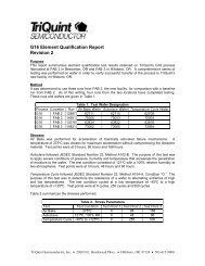
<strong>0.13</strong> <strong>um</strong> <strong>pHEMT</strong> (TQP13) Process Cross-section<br />
Self-align<br />
Ohmic<br />
<strong>pHEMT</strong><br />
General Description<br />
Air Bridge Global Plated Metal (5 <strong>um</strong>)<br />
Bell Metal Bell Metal MIM Bottom<br />
(1 <strong>um</strong>) (1 <strong>um</strong>)<br />
N+<br />
Pseudomorphic channel<br />
N+ Epi<br />
Resistor<br />
Semi-Insulating GaAs Substrate<br />
<strong>0.13</strong> <strong>um</strong> <strong>pHEMT</strong> Device Cross-Section<br />
Limited Release Process<br />
TQP13<br />
<strong>0.13</strong> <strong>um</strong> D <strong>pHEMT</strong> <strong>Foundry</strong> <strong>Service</strong><br />
Bell Metal<br />
Damage<br />
Isolation Implant<br />
MIM Capacitor<br />
<strong>TriQuint</strong>'s TQP13 process is a unique, low-cost 150mm wafer,<br />
optical lithography <strong>0.13</strong><strong>um</strong> <strong>pHEMT</strong> process used for low noise<br />
and medi<strong>um</strong> power applications in Ku-band through V-band applications.<br />
The process features a highly repeatable <strong>0.13</strong><strong>um</strong><br />
self-aligned gate <strong>pHEMT</strong> FET coupled with high density capacitors,<br />
epi resistors and 3 layers of gold interconnect. With typical<br />
Ft of 95 GHz, the process is used for V-band automotive radar<br />
and high frequency point to point radio applications. With typical<br />
NF < .5dB in Ku-band, the process is used for low cost LNB<br />
amplifier and convert blocks in cons<strong>um</strong>er Direct Broadcast Satellite<br />
dish systems. Simple to use, repeatable and highly competitive<br />
TQP13 is ideal for emerging cons<strong>um</strong>er mmWave applications.<br />
Page 1 of 4; Rev 0.1 1.0 2/09/2004<br />
11/8/2006<br />
Features<br />
• Low cost Optical Lithography<br />
<strong>0.13</strong><strong>um</strong> Gate<br />
• High Ft, ~95 GHz<br />
• Low Noise, < 0.5 dB in Ku-band<br />
• Interconnects: 2 Global (1 Airbridge)<br />
• High Value MIM Capacitor; 0.34<br />
fF/<strong>um</strong> 2<br />
• Epi Resistor; 105 Ώsq.<br />
• Backside Vias<br />
• High Vol<strong>um</strong>e 150 mm Wafers<br />
• Production Status<br />
• Design Kit available for Microwave<br />
Office (AWR)<br />
Applications<br />
• DBS LNB and Down Convert<br />
• Automotive Radar<br />
• Satellite Communications<br />
• Low Noise Point to Point/Point to<br />
Multipoint Radio LNA<br />
• High Frequency Medi<strong>um</strong> Power<br />
• High Frequency Mixer<br />
• Fiber Optic TIA and Driver,<br />
10Gb/s - 40Gb/s
TQP13<br />
Process<br />
Details<br />
Maxim<strong>um</strong><br />
Ratings<br />
<strong>TriQuint</strong> <strong>Semiconductor</strong><br />
2300 NE Brookwood Pkwy<br />
Hillsboro, Oregon 97124<br />
Limited Production Release Process<br />
TQP13<br />
<strong>0.13</strong> <strong>um</strong> D <strong>pHEMT</strong> <strong>Foundry</strong> <strong>Service</strong><br />
Process Details (Typical Specifications)<br />
Element Parameter Value Units<br />
D-Mode <strong>pHEMT</strong> Vp (1uA/<strong>um</strong>) -0.30 V<br />
Idss 100 mA/mm<br />
Gm (max) 700 mS/mm<br />
Breakdown, Vds 8 (typical)<br />
5.5 (min)<br />
Ft @ 250mA/mm 95 GHz<br />
Imax (Vgs=0.7 V) 450 mA/mm<br />
NF (12 GHz) < 0.5 dB<br />
Common Process Element Details<br />
Gate Length <strong>0.13</strong> μm<br />
Interconnect 2 Metal Layers<br />
MIM Caps Value 340 pF/mm2<br />
Resistors Epi 105 Ohms/sq<br />
Vias Yes<br />
Mask Layers No Vias 11<br />
With Vias 13<br />
Storage Temperature Range -65 to +150 Deg C<br />
Operating Temperature Range -55 to +150 Deg C<br />
<strong>Semiconductor</strong>s for Communications<br />
www.triquint.com<br />
Page Page 2 of 2 of 4; Rev 5; Rev 0.1 1.0 2.0 2/09/2004<br />
11/8/2006<br />
7/22/03<br />
V<br />
Phone: 503-615-9000<br />
Fax: 503-615-8905<br />
Email: info@triquint.com
TQP13<br />
Gm vs. Vgs<br />
TQP13<br />
Ft vs. Id<br />
<strong>TriQuint</strong> <strong>Semiconductor</strong><br />
2300 NE Brookwood Pkwy<br />
Hillsboro, Oregon 97124<br />
Gm (mS/mm)<br />
Limited Production Release Process<br />
TQP13<br />
<strong>0.13</strong> <strong>um</strong> D <strong>pHEMT</strong> <strong>Foundry</strong> <strong>Service</strong><br />
<strong>Semiconductor</strong>s for Communications<br />
www.triquint.com<br />
Page Page 3 of 3 of 4; Rev 5; Rev 0.1 1.0 2.0 2/09/2004<br />
11/8/2006<br />
7/22/03<br />
Phone: 503-615-9000<br />
Fax: 503-615-8905<br />
Email: info@triquint.com
Prototyping and Development<br />
• Prototype Development Quickturn (PDQ):<br />
• One-Quarter of a Shared Mask Set<br />
• Priority Start in Queue<br />
• See <strong>TriQuint</strong> website for bimonthly schedule<br />
• Prototype Wafer Option (PWO):<br />
• Customer-specific Masks, Customer Schedule<br />
• 2 wafers delivered<br />
• Priority Start in Queue<br />
Design Tool Status<br />
• Complete Design Manual Now<br />
• Device Library of circuit elements: FETs, diodes, bulk<br />
resistors, capacitors, inductors<br />
• Design Kit for ADS and Microwave Office (AWR)<br />
• Layout Library in GSD II format for Microwave Office<br />
and IC Editors<br />
• Layout Rule Sets for Design Rule Check in IC Editors<br />
• Package models for supported package styles<br />
Training<br />
• GaAs Design Classes:<br />
• Half Day Introduction; Upon Request<br />
• Three Day Technical Training; Fall & Spring at<br />
<strong>TriQuint</strong> Oregon facility<br />
• For Training & PDQ Schedules, please visit:<br />
www.triquint.com/foundry/<br />
<strong>TriQuint</strong> <strong>Semiconductor</strong><br />
2300 NE Brookwood Pkwy<br />
Hillsboro, Oregon 97124<br />
Limited Production Release Process<br />
TQP13<br />
<strong>0.13</strong> <strong>um</strong> D <strong>pHEMT</strong> <strong>Foundry</strong> <strong>Service</strong><br />
<strong>Semiconductor</strong>s for Communications<br />
www.triquint.com<br />
Page Page 4 of 4 of 4; Rev 5; Rev 1.0 2.0 11/8/2006 7/22/03<br />
Process Qualification Status<br />
• Mature, 150-mm process<br />
• Process released to production<br />
• Full 150mm wafer Process Qualification complete<br />
• For more information on Quality and Reliability, contact<br />
<strong>TriQuint</strong> or visit:<br />
www.triquint.com/manufacturing/QR/<br />
Applications Support <strong>Service</strong>s<br />
• Tiling of GDSII stream files including PCM<br />
• Design Rule Check services<br />
• Packaged Part Test Development Engineering:<br />
• Thermal Analysis Engineering<br />
• Yield Enhancement Engineering<br />
• Part Qualification <strong>Service</strong>s<br />
• Failure Analysis<br />
Manufacturing <strong>Service</strong>s<br />
• Mask Making<br />
• Production 150 Wafer Fab<br />
• Wafer Thinning; 10-, 7-, & 4-mil<br />
• Wafer Sawing<br />
• Substrate Vias– only with 4-mil wafer thickness<br />
• Vol<strong>um</strong>e DC Die Sort Testing<br />
• High Vol<strong>um</strong>e Plastic Packaging<br />
• High Vol<strong>um</strong>e RF Packaged Part Testing<br />
Please contact your local <strong>TriQuint</strong> <strong>Semiconductor</strong> Representative/ Distributor<br />
or Commercial <strong>Foundry</strong> <strong>Service</strong>s Marketing for Additional information:<br />
E-mail: sales@triquint.com; Phone: (503) 615-9000 Fax: (503) 615-8905<br />
Phone: 503-615-9000<br />
Fax: 503-615-8905<br />
Email: info@triquint.com