VPIN (Vertical P-I-N) GaAs Diode - TriQuint Semiconductor
VPIN (Vertical P-I-N) GaAs Diode - TriQuint Semiconductor
VPIN (Vertical P-I-N) GaAs Diode - TriQuint Semiconductor

You also want an ePaper? Increase the reach of your titles
YUMPU automatically turns print PDFs into web optimized ePapers that Google loves.
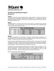
Contacts<br />
n-<strong>GaAs</strong>, 0.75 µm<br />
Semi-insulating <strong>GaAs</strong><br />
General Description<br />
500 West Renner Road<br />
Richardson, Texas 75080<br />
Ti/Pt/Au, 0.6 µm<br />
p-<strong>GaAs</strong>, 0.25 µm<br />
i-<strong>GaAs</strong>, 1.2 µm<br />
<strong>VPIN</strong> Structure Cross-Section<br />
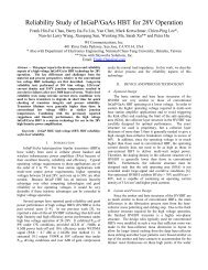
The <strong>VPIN</strong> (<strong>Vertical</strong> P-I-N) <strong>GaAs</strong> <strong>Diode</strong> process is excellent<br />
for low-loss limiters, switches, and phase shifters. Using<br />
this process, <strong>TriQuint</strong> has produced switches with high<br />
power handling capability, low on-state resistance, and low<br />
off-state capacitance. The higher cutoff frequency of the<br />
PIN diode element makes this switch ideal for broadband<br />
electronic components and communication systems. Passives<br />
include 2 thick-metal interconnect layers, precision<br />
TaN resistors, <strong>GaAs</strong> resistors, MIM capacitors and<br />
through-substrate vias. The via-under-cap process aids in<br />
size compaction and offers excellent grounds at higher frequencies.<br />
Air bridges produce minimal interconnect capacitance.<br />
<strong>VPIN</strong> (<strong>Vertical</strong> P-I-N) <strong>GaAs</strong> <strong>Diode</strong><br />
Process Data Sheet<br />
<strong>Semiconductor</strong>s for Communications, Space and Military<br />
www.<strong>TriQuint</strong>.com<br />
Page 1 of 3; 9/24/02<br />
Specifications are subject to change.<br />
Features<br />
• Multiple P-I-N diode sizes<br />
• Low on-state resistance<br />
• Low off-state capacitance<br />
• Device passivation<br />
• High Q passives<br />
• MIM capacitors<br />
• TaN resistors<br />
• 2 metal layers<br />
• Air bridges<br />
• Substrate vias<br />
Applications<br />
• Communications<br />
• Space<br />
• Military<br />
• Phase shifters<br />
• Limiters<br />
• Switches<br />
• Variable attenuators<br />
Phone: 972-994-8200<br />
Foundry: 972-994-4545<br />
Email: info@triquint.com
500 West Renner Road<br />
Richardson, Texas 75080<br />
<strong>VPIN</strong> (<strong>Vertical</strong> P-I-N) <strong>GaAs</strong> <strong>Diode</strong><br />
Process Data Sheet<br />
Element<br />
<strong>Diode</strong>s<br />
Parameter Typical Value Units<br />
MIM capacitors density 300 pF/mm 2<br />
<strong>VPIN</strong> Process Details<br />
Capacitors over vias yes<br />
TaN resistors sheet resistance 50 Ω/sq<br />
Vias yes<br />
Substrate thickness 100 µm<br />
<strong>VPIN</strong> Models Available<br />
Size (µm) Layout Type Substrate (µm)<br />
15 round 100<br />
25 round 100<br />
30 round 100<br />
Application Examples<br />
DC to 20 GHz SP4T PIN Switch TGS 2304-SCC:<br />
The <strong>TriQuint</strong> TGA2304-SCC is a <strong>GaAs</strong> monolithic P-I-N diode single-pole, four-throw switch that<br />
operates from DC to 20 GHz. At a bias current of 10 mA per output arm, typical midband performance<br />
is 0.6 dB insertion loss with 40 dBm isolation in the off-arms. Isolation and insertion loss can<br />
be adjusted by varying the output arm bias current of the switch.<br />
Wideband Dual Stage Limiter TGL 2201:<br />
This limiter is a 3 to 25 GHz limiter with less than 0.75 dB loss at X-band and 15 dB return losses.<br />
The limiter's RF leakage is less than 18 dBm at 1 W Pin and it has an input power survivability<br />
greater than 5 W.<br />
<strong>Semiconductor</strong>s for Communications, Space and Military<br />
www.<strong>TriQuint</strong>.com<br />
Page 2 of 3; 9/24/02<br />
Specifications are subject to change.<br />
Phone: 972-994-8200<br />
Foundry: 972-994-4545<br />
Email: info@triquint.com
Prototyping and Development<br />
• Prototype Wafer Option (PWO)<br />
• Customer-specific masks<br />
• Customer schedule<br />
• 2 wafers delivered<br />
• Backside via process included<br />
• PCM (process control monitor) qualified<br />
wafers<br />
Design Tools<br />
• Device libraries of circuit elements:<br />
• <strong>Diode</strong>s<br />
• Thin-film resistors<br />
• Capacitors<br />
• Inductors<br />
• Agilent ADS design kit<br />
Training<br />
• <strong>GaAs</strong> design classes:<br />
• Half-day introduction upon request<br />
• 3-day technical training upon request at<br />
the <strong>TriQuint</strong> Texas facility<br />
500 West Renner Road<br />
Richardson, Texas 75080<br />
<strong>VPIN</strong> (<strong>Vertical</strong> P-I-N) <strong>GaAs</strong> <strong>Diode</strong><br />
Process Data Sheet<br />
<strong>Semiconductor</strong>s for Communications, Space and Military<br />
www.<strong>TriQuint</strong>.com<br />
Page 3 of 3; 9/24/02<br />
Specifications are subject to change.<br />
Process Status<br />
• <strong>VPIN</strong> (<strong>Vertical</strong> P-I-N) <strong>GaAs</strong> <strong>Diode</strong> is fully released<br />
and qualified<br />
Contact <strong>TriQuint</strong> or visit<br />
http://www.triquint.com/company/quality/<br />
for more information on quality and reliability.<br />
Applications Services<br />
• Tiling of GDSII stream files including PCM<br />
(process control monitor)<br />
• Design rule checking<br />
• Layout versus schematic checking<br />
• Engineering:<br />
• On-wafer DC test<br />
• On-wafer RF test<br />
• Thermal analysis<br />
• Yield enhancement<br />
• Part qualification<br />
• Failure analysis<br />
• Space Qualification<br />
Manufacturing Services<br />
• Mask making<br />
• Wafer thinning<br />
• Wafer dicing<br />
• Substrate vias<br />
• DC die-sort testing<br />
• RF die-sort testing<br />
• Final visual testing<br />
Phone: 972-994-8200<br />
Foundry: 972-994-4545<br />
Email: info@triquint.com