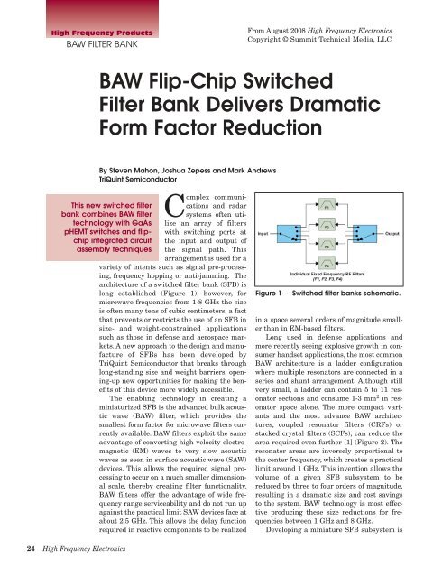
BAW Flip-Chip Switched Filter Bank Delivers Dramatic Form Factor ...
BAW Flip-Chip Switched Filter Bank Delivers Dramatic Form Factor ...
BAW Flip-Chip Switched Filter Bank Delivers Dramatic Form Factor ...

Create successful ePaper yourself
Turn your PDF publications into a flip-book with our unique Google optimized e-Paper software.
High Frequency Products<br />
<strong>BAW</strong> FILTER BANK<br />
24 High Frequency Electronics<br />
<strong>BAW</strong> <strong>Flip</strong>-<strong>Chip</strong> <strong>Switched</strong><br />
<strong>Filter</strong> <strong>Bank</strong> <strong>Delivers</strong> <strong>Dramatic</strong><br />
<strong>Form</strong> <strong>Factor</strong> Reduction<br />
By Steven Mahon, Joshua Zepess and Mark Andrews<br />
TriQuint Semiconductor<br />
Complex communi-<br />
This new switched filter cations and radar<br />
bank combines <strong>BAW</strong> filter systems often uti-<br />
technology with GaAs lize an array of filters<br />
pHEMT switches and flip- with switching ports at<br />
chip integrated circuit the input and output of<br />
assembly techniques the signal path. This<br />
arrangement is used for a<br />
variety of intents such as signal pre-processing,<br />
frequency hopping or anti-jamming. The<br />
architecture of a switched filter bank (SFB) is<br />
long established (Figure 1); however, for<br />
microwave frequencies from 1-8 GHz the size<br />
is often many tens of cubic centimeters, a fact<br />
that prevents or restricts the use of an SFB in<br />
size- and weight-constrained applications<br />
such as those in defense and aerospace markets.<br />
A new approach to the design and manufacture<br />
of SFBs has been developed by<br />
TriQuint Semiconductor that breaks through<br />
long-standing size and weight barriers, opening-up<br />
new opportunities for making the benefits<br />
of this device more widely accessible.<br />
The enabling technology in creating a<br />
miniaturized SFB is the advanced bulk acoustic<br />
wave (<strong>BAW</strong>) filter, which provides the<br />
smallest form factor for microwave filters currently<br />
available. <strong>BAW</strong> filters exploit the same<br />
advantage of converting high velocity electromagnetic<br />
(EM) waves to very slow acoustic<br />
waves as seen in surface acoustic wave (SAW)<br />
devices. This allows the required signal processing<br />
to occur on a much smaller dimensional<br />
scale, thereby creating filter functionality.<br />
<strong>BAW</strong> filters offer the advantage of wide frequency<br />
range serviceability and do not run up<br />
against the practical limit SAW devices face at<br />
about 2.5 GHz. This allows the delay function<br />
required in reactive components to be realized<br />
From August 2008 High Frequency Electronics<br />
Copyright © Summit Technical Media, LLC<br />
Figure 1 · <strong>Switched</strong> filter banks schematic.<br />
in a space several orders of magnitude smaller<br />
than in EM-based filters.<br />
Long used in defense applications and<br />
more recently seeing explosive growth in consumer<br />
handset applications, the most common<br />
<strong>BAW</strong> architecture is a ladder configuration<br />
where multiple resonators are connected in a<br />
series and shunt arrangement. Although still<br />
very small, a ladder can contain 5 to 11 resonator<br />
sections and consume 1-3 mm 2 in resonator<br />
space alone. The more compact variants<br />
and the most advance <strong>BAW</strong> architectures,<br />
coupled resonator filters (CRFs) or<br />
stacked crystal filters (SCFs), can reduce the<br />
area required even further [1] (Figure 2). The<br />
resonator areas are inversely proportional to<br />
the center frequency, which creates a practical<br />
limit around 1 GHz. This invention allows the<br />
volume of a given SFB subsystem to be<br />
reduced by three to four orders of magnitude,<br />
resulting in a dramatic size and cost savings<br />
to the system. <strong>BAW</strong> technology is most effective<br />
producing these size reductions for frequencies<br />
between 1 GHz and 8 GHz.<br />
Developing a miniature SFB subsystem is
High Frequency Products<br />
<strong>BAW</strong> FILTER BANK<br />
Figure 2 · CRF or SCF Bulk Acoustic<br />
Wave <strong>Filter</strong> (1.5 x 0.75 mm)<br />
enabled by combining three different<br />
technologies: <strong>BAW</strong> <strong>Filter</strong>s, GaAs<br />
pHEMT switches and Au/Sn flip-chip<br />
assembly. A configuration of an SFB<br />
with 4 filters is approximately 5 × 5 ×<br />
1 mm in a surface mount module<br />
package. Using E/D pHEMT technology<br />
affords the capability of adding<br />
digital switch decoders to minimize<br />
the number of control lines required.<br />
Configuration<br />
<strong>BAW</strong> filter die are fabricated for<br />
the specific frequency responses<br />
desired. The die can be tested in<br />
advance of assembly to assure a<br />
known good filter. The switch IC die<br />
is designed such that there is a top<br />
level metal pattern matching the solder<br />
ring and I/O of the acoustic filter.<br />
A key requirement of a <strong>BAW</strong> filter is<br />
the necessity for a hermetic cavity<br />
environment to allow proper acoustic<br />
resonance and long-term stability. A<br />
hermetic seal can be accomplished<br />
with a high temperature solder<br />
stand-off that can be made as part of<br />
the <strong>BAW</strong> filter itself. This standoff is<br />
electroplated around the perimeter of<br />
the die and provides I/O and ground<br />
connections (Figure 2). The switch die<br />
can also be pre-tested to assure functionality.<br />
The <strong>BAW</strong> die is flip-chip<br />
assembled to its matching pattern on<br />
the switch IC and put through a solder<br />
reflow process. The flip-chip<br />
26 High Frequency Electronics<br />
Figure 3 · Switch die with filter mating<br />
patterns. <strong>BAW</strong> filters (rectangular<br />
devices to the left and right of<br />
the pHEMT switch die), are flipped<br />
for mounting to their receiving<br />
points on the GaAs circuits.<br />
attach not only provides the hermetic<br />
capability but provides for minimal<br />
parasitics. The resulting assembly is<br />
then ready for the next level of board<br />
or module chip and wire assembly.<br />
A miniature SFB offers several<br />
key benefits that resolve size, weight<br />
and performance challenges compared<br />
to existing, large form factor<br />
SFB assemblies. Currently, the most<br />
“compact” approach is to use existing<br />
filters of various architectures and<br />
route to external switches in a module<br />
or printed circuit board. Using<br />
die-to-die, flip-chip assembly solves<br />
three issues at the same time. First,<br />
the size can be made much smaller,<br />
which allows several orders of magnitude<br />
in volume reduction. Second, the<br />
close proximity of the filter to the<br />
switch allows for a minimization of<br />
parametric losses in the RF circuit<br />
where switch-to-filter routing is an<br />
issue. Third, minimizing the list of<br />
materials and the smaller size will<br />
result in a lower cost per filter bank<br />
function.<br />
Two major challenges, one in system<br />
design and the other in flip-chip<br />
assembly, had to be resolved in order<br />
to create fully functional miniature<br />
SFBs. An example of one system<br />
design challenge can be found in the<br />
fact that a <strong>BAW</strong> device requires<br />
Figure 4 · The assembled miniature<br />
switched filter bank with two filters<br />
robust grounding, as common ground<br />
inductance can degrade the filter performance.<br />
The pHEMT switch die<br />
creates one more interface between<br />
the filter and the application board,<br />
thus creating a potential problem.<br />
This was addressed by using a significant<br />
number of through-wafer via<br />
ground connections, available as a<br />
benefit of using the pHEMT process.<br />
The assembly process offers challenges<br />
due to the small scale and the<br />
requirement for a complete seal<br />
around the perimeter of the filter.<br />
The exact metallurgical balance of<br />
the gold and tin must be maintained<br />
as well as time, temperature and<br />
attach pressure. An example of the<br />
importance of balance in this situation<br />
can be found in the fact that<br />
excessive tin can cause shorting<br />
between ground and I/O nodes,<br />
whereas insufficient tin will result in<br />
a weak mechanical attach. Modern<br />
IC and flip-chip assembly technology<br />
and equipment provide sufficient<br />
capability to maintain these process<br />
parameters to the tolerances<br />
required.<br />
Test Results<br />
A two-channel miniature SFB<br />
prototype was fabricated around the<br />
GPS L1 frequency (Figure 4) of 1.575<br />
GHz. Two SCF <strong>BAW</strong> filters were fabricated<br />
for frequencies 30 MHz apart.<br />
These filters are 1.50 × 0.75 mm in<br />
size. Their performance, when assembled<br />
with the pHEMT switches as a
High Frequency Products<br />
<strong>BAW</strong> FILTER BANK<br />
Figure 5a · Magnitude of S21 for<br />
both channels overlaid.<br />
two-filter system, is shown in Figure<br />
5. The stand alone <strong>BAW</strong> filters maintain<br />
an insertion loss (IL) of 1.5 dB.<br />
Each switch contributes about 0.6<br />
dB, resulting in a system insertion<br />
loss of less than 3 dB. The interconnection<br />
and other parasitics have little<br />
additional contribution to overall<br />
loss. The crossover interaction<br />
between filters is particularly low.<br />
This demonstration provides solid<br />
insight and direction as a means to<br />
build more complex SFB designs.<br />
Figure 6 shows the demonstrated<br />
wideband performance of a single<br />
channel.<br />
Summary<br />
The integration of TriQuint’s compact<br />
<strong>BAW</strong> filters and GaAs pHEMT<br />
switches has resulted in the creation<br />
of a miniature switched filter bank<br />
Fig. 6: Wideband performance of a<br />
single channel of the miniature<br />
switched filter bank<br />
28 High Frequency Electronics<br />
Figure 5b · S21 (passband magnification)<br />
for both channels overlaid.<br />
(SFB) that can enable new approaches<br />
to system architectures for<br />
advanced RF systems. Immediate<br />
applications expected to benefit from<br />
this advancement include a variety of<br />
intents such as signal pre-processing,<br />
frequency hopping or anti-jamming<br />
functions for defense and aerospace<br />
markets. Because such devices provide<br />
a dramatic reduction in size<br />
while retaining essential performance<br />
capabilities it’s possible to<br />
envision switched filter bank functionality<br />
in applications far beyond<br />
their current range. A miniature<br />
SFB’s size and performance also<br />
opens new doors for markets and<br />
applications by simplifying integration<br />
both at architecture and system<br />
levels.<br />
Cost and yield will improve as<br />
this technology advances. Such<br />
advances will also help enable new<br />
capabilities tied to the number of<br />
channels that can be switched by a<br />
single device. For example: pHEMT<br />
switches with single pole, nine-throw<br />
(SP9T) designs are now used in wireless<br />
handsets. As more designers are<br />
exposed to the possibilities of using<br />
miniature switched filter banks, one<br />
can imagine a standard pHEMT<br />
switch die that allows a wide range of<br />
custom filter combinations to be<br />
made with modest development. A<br />
limit on the number of filters possible<br />
in a bank is not set in a literal sense,<br />
but is typically governed by classical<br />
Figure 5c · Return Loss of both<br />
channels overlaid.<br />
system partitioning needs. Growing<br />
the number of channels that can be<br />
switched by a single device in mobile<br />
handset applications points to the<br />
possibility that miniature SFBs will<br />
also advance in such a way, offering<br />
new solutions to designers of<br />
advanced RF systems.<br />
The size and cost advantages provided<br />
by miniature SFBs compared to<br />
current technology leads the imagination<br />
to jump from obvious first-generation<br />
applications in defense and<br />
advanced aerospace markets to commercial<br />
intents. Competitive pressures<br />
in commercial markets will also<br />
drive development and speed product<br />
evolution. As the market has demonstrated<br />
with other breakthrough technologies,<br />
a range of initial applications<br />
grows very quickly once the<br />
ingenuity of systems designers is<br />
brought to bear, which will enable<br />
miniature SFBs to serve an everincreasing<br />
universe of applications.<br />
References<br />
1. K.M. Lakin, J. Belsick, J.F.<br />
McDonald, and K.T. McCarron,<br />
“High Performance Stacked Crystal<br />
<strong>Filter</strong>s for GPS and Wide Bandwidth<br />
Applications,” IEEE 2001 Ultrasonics<br />
Symposium, October 9, 2001<br />
TriQuint Semiconductor<br />
Tel: +1 541-382-6706<br />
E-mail: baw-sfb@tqs.com<br />
www.triquint.com