TQP15 40 GHz PA - TriQuint Semiconductor
TQP15 40 GHz PA - TriQuint Semiconductor
TQP15 40 GHz PA - TriQuint Semiconductor

Create successful ePaper yourself
Turn your PDF publications into a flip-book with our unique Google optimized e-Paper software.
A <strong>40</strong> <strong>GHz</strong> Power Amplifier Using a Low Cost High Volume 0.15 um<br />
Optical Lithography pHEMT Process<br />
Kenneth W. Mays<br />
<strong>TriQuint</strong> <strong>Semiconductor</strong>, Hillsboro, Oregon, 97224, USA<br />
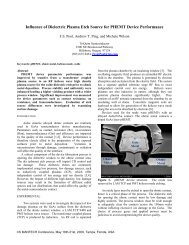
Abstract — A <strong>40</strong> <strong>GHz</strong> power amplifier is realized with a new<br />
0.15 um optical lithography pHEMT process developed for lowcost<br />
microwave and millimeter wave circuits. Several Ka and V<br />
Band market requirements have driven demand for higher<br />
bandwidth, low-cost, integrated circuits. A <strong>40</strong> <strong>GHz</strong> power<br />
amplifier is used to demonstrate the process capabilities, starting<br />
from the initial design phase and culminating with the<br />
fabrication and measurement of the solid state power amplifier.<br />
Index Terms — Microstrip components, millimeter wave power<br />
amplifier, pHEMT, impedance matching.<br />
I. INTRODUCTION<br />
A <strong>40</strong> <strong>GHz</strong> power amplifier has been designed and<br />
fabricated using a 0.15 um optical lithography pseudomorphic<br />
high electron mobility transistor (pHEMT). The high volume<br />
150 mm process named <strong>TQP15</strong>, has been developed by<br />
<strong>TriQuint</strong> <strong>Semiconductor</strong> to meet increased demand for<br />
microwave and millimeter wave integrated circuits with good<br />
power performance at higher frequencies. The amplifier has<br />
been designed for 15 dB of gain and 28 dBm of output power<br />
from a 3 V power supply. Related market applications<br />
include Automotive Radar, Point-to-Point Radio, VSAT, and<br />
other Ka and V band applications. Several papers have<br />
reported amplifier performance in the Ka and Q bands, [1] –<br />
[8], but these amplifiers use direct write e-beam gates and airbridge<br />
interconnect, technologies less suitable for high<br />
volume low cost manufacturing.<br />
The simulation, fabrication and measurement of the amplifier<br />
demonstrate the process capability. DC and RF measurements<br />
and load pull data, tuned for power, illustrating the gain and<br />
power added efficiency (<strong>PA</strong>E) are presented.<br />
A description of the design and performance of the 3-stage<br />
power amplifier (<strong>PA</strong>) is presented. Transistor cell DC and RF<br />
characteristics, impedance transformations and matching<br />
networks are described.<br />
II. PROCESS AND MODEL OVERVIEW<br />
The <strong>TriQuint</strong> <strong>TQP15</strong> process is a refractory gate technology<br />
that is fabricated on 150 mm diameter 100 um thick GaAs<br />
wafers with substrate via holes. <strong>TQP15</strong> is an extension of the<br />
work performed to develop the TQP25 [9] and TQP13 [10]<br />
process technologies. These processes use I-line steppers and<br />
sidewall spacer gate construction for high throughput and<br />
low-cost manufacturing.<br />
A summary of the process parameters is presented in Table<br />
I.<br />
TABLE I<br />
<strong>TQP15</strong> PROCESS SUMMARY<br />
Process Specifications, Vds = 3.0 V<br />
Parameter Typical Value Units<br />
Lg 0.15 um<br />
Vp -1.0 V<br />
BV min/typ 12/14 V<br />
Imax/Idss 550 / 310 mA/mm<br />
Gm 450 @ Idss mS/mm<br />
Ft / Fmax 65 / 125 @ Idss<br />
Process Passive Elements<br />
<strong>GHz</strong><br />
Parameter Typical Value Units<br />
Resistors 50 / 225 Ω/sq<br />
BLMET<br />
(0.62um)<br />
50 mΩ/sq<br />
Met 2 (4um) 6 mΩ/sq<br />
MIM Cap 0.62 fF/um 2<br />
The <strong>TQP15</strong> optical gate technology enables a less<br />
expensive solution for the design space. The refractory gate<br />
enhances the thermal stability and the long term reliability of<br />
the transistor. A scanning electron microscopy image of the<br />
gate structure is shown in figure 1.<br />
Fig. 1. Cross-Section Image of Gate<br />
This material is presented to ensure timely dissemination of scholarly and technical work. Copyright and all rights therein are<br />
retained by authors or by other copyright holders. All persons copying this information are expected to adhere to the terms and<br />
constraints invoked by each author's copyright. In most cases, these works may not be reposted without the explicit permission of<br />
the copyright holder."
The planarized benzocyclobutene (BCB) interlayer<br />
dielectric provides more uniform electrical performance for<br />
different packaging conditions, as compared to the more<br />
typical air-bridge process. A pictorial of the process cross<br />
section, with active and passive components, is shown in<br />
figure 2.<br />
Fig. 2. Process Cross-Section of <strong>TQP15</strong><br />
Initial device characterization and models were derived<br />
from the coplanar waveguide (CPW) ground-signal-ground<br />
(GSG) test configuration shown in figure 3.<br />
Fig. 3. 4 x 50 FET in a CPW Test Structure<br />
Further characterization and modeling were derived from<br />
test configurations using substrate via holes and microstrip<br />
launches. Associated on-wafer LRM calibration structures<br />
were included. Figure 4 shows a ten finger device with a gate<br />
width of 60 um.<br />
Fig. 4. 10 x 60 FET in Microstrip GSG Test Structure<br />
III. DESIGN METHODOLOGY<br />
The <strong>PA</strong> was designed using the <strong>TQP15</strong> Process Design Kit<br />
(PDK) with a commercially available harmonic balance<br />
simulator. The TOM4 pHEMT model was extracted from DC<br />
and multiple bias S-parameter measurements. The resulting<br />
component model accuracy improves agreement between<br />
simulation and measurement of the fabricated amplifier.<br />
A microstrip line approach was selected in place of CPW to<br />
avoid excessive metallization and potential transmission line<br />
modeling problems.<br />
The output stage was designed to deliver over 28 dBm of<br />
output power from eight unit cells of 10 x 80 um each. The<br />
driver and second stage use 10 x 60 um cells for appropriate<br />
gain and output power. The gate periphery ratio of stages 1,<br />
2, and 3 is 1:2:2.75. The die size is 3.1 mm by 3.1 mm, driven<br />
primarily by the size of the third stage transistor. A picture of<br />
the die is shown in figure 5.<br />
This material is presented to ensure timely dissemination of scholarly and technical work. Copyright and all rights therein are<br />
retained by authors or by other copyright holders. All persons copying this information are expected to adhere to the terms and<br />
constraints invoked by each author's copyright. In most cases, these works may not be reposted without the explicit permission of<br />
the copyright holder."
Fig. 5. Power Amplifier MMIC<br />
A larger output current is required to generate the required<br />
28 dBm of output power from the relatively low supply<br />
voltage of 3 V. In addition to the device size, the larger<br />
output current requirement results in low output impedance<br />
for the third stage transistor which must be impedance<br />
matched to a 50 Ohm system impedance. Microstrip<br />
transmission lines were designed to provide the proper<br />
impedance transformation between stages and for the<br />
specified 50 Ohm input and output impedances.<br />
The DC drain supply current feed is integrated into the<br />
output matching circuit which requires the microstrip<br />
transmission lines to be sized appropriately for the DC current<br />
as well as the impedance transformation. The biasing network<br />
is symmetrically fed to minimize phase differences. The<br />
matching and DC feed networks employ MIM capacitors and<br />
thin film resistors in addition to the microstrip transmission<br />
lines.<br />
The thin film resistors are used to suppress and prevent inband<br />
and odd mode oscillations, especially in power combing<br />
configurations as described in [2],[3], and [7]. The resistive<br />
elements are used in series between the parallel drains in the<br />
output cell.<br />
A low voltage high power design at high frequencies is<br />
complicated by the steep load line restrictions and the low<br />
impedance required for obtaining the required output power.<br />
The gate voltage is set to hold a predetermined drain current<br />
for power efficient deep class AB operation. Power efficient<br />
operation, matching circuit, and bandwidth limitations are<br />
more thoroughly addressed in [4].<br />
IV. MEASUREMENTS<br />
Two test transistors were used to compare simulated<br />
performance to measured performance. The simulated versus<br />
measured results are shown here. The simulated and<br />
measured performance of the complete three stage <strong>40</strong> <strong>GHz</strong><br />
amplifier will be shown in the oral presentation of this paper.<br />
The DC I-V characteristics of the 4 x <strong>40</strong> um pHEMT are<br />
simulated using the TOM4 model and compared to the<br />
measured characteristics. The results are shown in figure 6.<br />
Measurements were taken on a process nominal full thickness<br />
wafer at room temperature.<br />
This material is presented to ensure timely dissemination of scholarly and technical work. Copyright and all rights therein are<br />
retained by authors or by other copyright holders. All persons copying this information are expected to adhere to the terms and<br />
constraints invoked by each author's copyright. In most cases, these works may not be reposted without the explicit permission of<br />
the copyright holder."<br />
0.1<br />
<strong>TQP15</strong> D4x50<br />
Meas.<br />
Data<br />
Sim.<br />
Fig. 6. IV Curves for the 4 x 50 Depletion Mode pHEMT FET<br />
Simulated and measured transconductance and drain current<br />
versus gate voltages ( -1.2 V to +0.8 V) are shown in figure 7.<br />
Gm dc (S)<br />
Ids (A)<br />
0.1<br />
0.08<br />
0.06<br />
0.04<br />
0.02<br />
0.08<br />
0.06<br />
0.04<br />
0.02<br />
-0<br />
0 2 4 6<br />
<strong>TQP15</strong> D4x50<br />
Vds = 2V<br />
Gm_dc<br />
Vgs= + 0.4V<br />
Vds (V)<br />
Vgs=0V<br />
Vgs=-0.2V<br />
0<br />
0<br />
-1.2 -0.8 -0.4 0.0 0.4 0.8<br />
Vgs (V)<br />
Fig. 7. DC Drain Current and Transconductance at Vds=2V<br />
(measured data marked with symbols)<br />
Ids<br />
-0.4V<br />
-0.6V<br />
Vgs=-0.8V<br />
0.1<br />
0.08<br />
0.06<br />
0.04<br />
0.02<br />
Ids (A)
S-Parameter measurements for three volt operation through<br />
50 <strong>GHz</strong> are shown in figure 8.<br />
Simulation..S(2,2)<br />
Simulation..S(1,1)<br />
Measured..S(2,2)<br />
Measured..S(1,1)<br />
freq (500.0MHz to 50.00<strong>GHz</strong>)<br />
Fig. 8. S11 (Circles) and S22 (Squares) are Measured Data and S11<br />
(Crosses) and S22 (Triangles) are Model Simulations<br />
Additional S-parameter measurements were made using 100<br />
um thick wafers with substrate via holes at the ground pads<br />
and at the pHEMT source (figure 4). The Maximum<br />
Available Gain (MSG) from 500 MHz to 50 <strong>GHz</strong> is shown in<br />
Figure 9. The MSG/MAG transition is above 30 <strong>GHz</strong>, with<br />
the substrate via holes in the ground path.<br />
Fig. 9. Maximum Gain Plot to 50 <strong>GHz</strong><br />
Load pull data has been measured. Figure 10 shows the<br />
gain and Power Added Efficiency (<strong>PA</strong>E) performance at 21<br />
<strong>GHz</strong>.<br />
<strong>TQP15</strong> P‐out, Gain, <strong>PA</strong>E vs P_in (Max <strong>PA</strong>E, 21 <strong>GHz</strong>)<br />
This material is presented to ensure timely dissemination of scholarly and technical work. Copyright and all rights therein are<br />
retained by authors or by other copyright holders. All persons copying this information are expected to adhere to the terms and<br />
constraints invoked by each author's copyright. In most cases, these works may not be reposted without the explicit permission of<br />
the copyright holder."<br />
P_out (dBm), Gain (dB)<br />
25<br />
20<br />
15<br />
10<br />
5<br />
0<br />
300 um (6x50)<br />
21 <strong>GHz</strong>, 6V, 30 mA<br />
4 mil with SVIAs<br />
Gs=0.658,
Gain (dB) & Pout (dBm)<br />
<strong>40</strong><br />
35<br />
30<br />
25<br />
20<br />
15<br />
10<br />
5<br />
0<br />
8 10 12 14 16 18 20 22 24 26<br />
Pin (dBm)<br />
Fig. 12. Simulated Gain (Squares), <strong>PA</strong>E (Circles), and Pout<br />
(Triangles) for the 3 Stage Amplifier<br />
35<br />
30<br />
25<br />
20<br />
15<br />
10<br />
5<br />
<strong>PA</strong>E (%)<br />
REFERENCES<br />
[1] Jeffrey A. Lester, W. L. Jones, and P. D. Chow, “High<br />
Performance MMIC 20 <strong>GHz</strong> LNA and 44 <strong>GHz</strong> Power Amplifier<br />
Using Planar-Doped InGaAs HEMTs ”, 1991 IEEE MTT-S Int.<br />
Microwave Symp. Dig., vol. 2, pp 433-436, June 1991.<br />
[2] W. Boulais, R.S. Donahue, A. Platzker, J. Huang, L. Aucoin, S.<br />
Shanfield, and M. Vafiades, “A High Power Q-Band GaAs<br />
Pseudomorphic HEMT Monolithic Amplifier”, 1994 IEEE<br />
MTT-S Int. Microwave Symp. Dig., vol. 2, pp 649-652, June<br />
1994.<br />
[3] James C. L. Chi, J. A. Lester, Y. Hwang, P. D. Chow, and M. Y.<br />
Huang, “A 1-W High Efficiency Q-Band MMIC Power<br />
Amplifier ”, IEEE Microwave and Guided Wave Letters, vol. 5,<br />
no. 1, pp 21-23, January 1995.<br />
[4] Youngwoo Kwon, Kyungjin Kim, Emilio A. Sovero, and Don<br />
S. Deakin, “Watt-Level Ka- and Q-Band MMIC Power<br />
Amplifiers Operating at Low Voltages”, IEEE Transactions on<br />
Microwave Theory and Techniques, vol. 48, no. 6, pp 891-897,<br />
June 2000.<br />
V. SUMMARY [5] O. Houbloss, D. Bourreau, A. Peden, B. Della, and R. Jezequel,<br />
This work describes a three stage <strong>40</strong> <strong>GHz</strong> power amplifier<br />
design using the <strong>TQP15</strong> 0.15 um high volume optical<br />
lithography pHEMT process. The work presented in this<br />
paper was used as a vehicle to provide information for <strong>PA</strong><br />
applications at <strong>40</strong> <strong>GHz</strong> and to demonstrate the ability to<br />
design and fabricate a <strong>PA</strong> through a standard design flow<br />
using a low-cost high-volume manufacturing process.<br />
A 28 dBm output power amplifier operating at 3 volts with<br />
a small signal gain of over 15 dB has been demonstrated.<br />
Simulated and measured performance of the circuit<br />
components has been shown. Simulated and measured<br />
performance of the complete three stage amplifiers will be<br />
shown in the oral presentation. Future work includes the<br />
investigation of performance improvement from slotted<br />
substrate via holes directly under the source contacts, and<br />
integrated active bias networks.<br />
ACKNOWLEDGEMENT<br />
I would like to thank my colleagues at <strong>TriQuint</strong> in<br />
Richardson and Hillsboro for their assistance, support, and<br />
patience.<br />
“Design of Broadband Ka Band Spatial Power Amplifiers”,<br />
2005 European Microwave Conference, vol. 1, 4 pp, October<br />
This material is presented to ensure timely dissemination of scholarly and technical work. Copyright and all rights therein are<br />
retained by authors or by other copyright holders. All persons copying this information are expected to adhere to the terms and<br />
constraints invoked by each author's copyright. In most cases, these works may not be reposted without the explicit permission of<br />
the copyright holder."<br />
2005.<br />
[6] Francois Y. Colomb and Aryeh Platzker, “2 and 4 Watt Ka-band<br />
GaAs PHEMT Power Amplifier MMICs”, 2003 IEEE MTT-S<br />
Int. Microwave Symp. Dig., vol. 2, pp 843-846, June 2003.<br />
[7] Shuoqi Chen, Sabyasachi Nayak, Ming-Yih Kao, and Joseph<br />
Delaney, “A Ka/Q-Band 2 Watt MMIC Power Amplifier Using<br />
Dual Recess 0.15 um PHEMT Process”, 2004 IEEE MTT-S Int.<br />
Microwave Symp. Dig., vol. 3, pp 1669-1672, June 2004.<br />
[8] A. Bessemoulin, S. Mahon, A. Dadello, G. McCulloch, and J.<br />
Harvey, “Compact and Broadband Microstrip Power Amplifier<br />
MMIC with <strong>40</strong>0-mW Output Power using 0.15-um GaAs<br />
PHEMTs”, 2005 European Gallium Arsenide and Other<br />
<strong>Semiconductor</strong> Application Symposium, pp 41-44, October<br />
2005.<br />
[9] Andrew T. Ping, Wolfgang Liebl, Gerard Mahoney, Steve<br />
Mahon, and Otto Berger, “A High-Performance 0.13-um<br />
AlGaAs/InGaAs pHEMT Process Using Sidewall Spacer<br />
Technology”, 2005 CS Mantech.<br />
[10] Corey Nevers, Andrew T. Ping, Tertius Rivers, Sumir Varma,<br />
Fred Pool, Moreen Minkoff, Ed Etzkorn, and Otto Berger,<br />
“High-Volume 0.25 um AlGaAs/InGaAs E/D pHEMT Process<br />
Utilizing Optical Lithography”, 2008 CS Mantech.