

End-Coupled, Half-Wavelength Resonator Filters - Design theory
End-Coupled, Half-Wavelength Resonator Filters - Design theory
End-Coupled, Half-Wavelength Resonator Filters - Design theory

You also want an ePaper? Increase the reach of your titles
YUMPU automatically turns print PDFs into web optimized ePapers that Google loves.
Microwave Filter <strong>Design</strong><br />
Chp. 5 Bandpass Filter<br />
Prof. Tzong-Lin Wu<br />
Department of Electrical Engineering<br />
National Taiwan University<br />
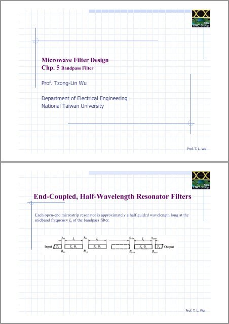
<strong>End</strong>-<strong>Coupled</strong>, <strong>Half</strong>-<strong>Wavelength</strong> <strong>Resonator</strong> <strong>Filters</strong><br />
Each open-end microstrip resonator is approximately a half guided wavelength long at the<br />
midband frequency f 0 of the bandpass filter.<br />
Prof. T. L. Wu<br />
Prof. T. L. Wu
<strong>End</strong>-<strong>Coupled</strong>, <strong>Half</strong>-<strong>Wavelength</strong> <strong>Resonator</strong> <strong>Filters</strong><br />
- Equivalent model<br />
What kind of resonator ? Why?<br />
<strong>End</strong>-<strong>Coupled</strong>, <strong>Half</strong>-<strong>Wavelength</strong> <strong>Resonator</strong> <strong>Filters</strong><br />
- <strong>Design</strong> <strong>theory</strong><br />
1. Find J-inverter values (half-wavelength resonator)<br />
Z in<br />
Z L<br />
Prof. T. L. Wu<br />
Prof. T. L. Wu
<strong>End</strong>-<strong>Coupled</strong>, <strong>Half</strong>-<strong>Wavelength</strong> <strong>Resonator</strong> <strong>Filters</strong><br />
- <strong>Design</strong> <strong>theory</strong><br />
Zin ZL ⎛ ω ⎞<br />
ZL + jZ0<br />
tan ⎜π ⎟<br />
ω0<br />
1 1<br />
Zin = Z<br />
⎝ ⎠<br />
0<br />
= =<br />
⎛ ω ⎞<br />
ω ( )<br />
Z0 Z tan<br />
jY0<br />
tan( )<br />
jB ω<br />
+ j<br />
π<br />
L ⎜π ⎟<br />
⎝ ω ω<br />
0 ⎠<br />
0 ZL<br />
= ∞<br />
ω near ω0<br />
Susceptance slope parameters<br />
ω dB 0 ( ω)<br />
ω0 1 π<br />
0π 0<br />
ω ω<br />
Y0b1FBW Y0FBW π π FBW<br />
bi = = Y = Y<br />
J01 = = Y0 = Y0<br />
2 2 2<br />
Ω g g Ω g g 2 2 g g<br />
d ω= ω0<br />
2. Find the susceptance of series gap capacitance<br />
0<br />
c 0 1 c 0 1 Ω 1<br />
0 1<br />
c =<br />
FBW b b π FBW<br />
J = = Y<br />
i i+<br />
1<br />
i, i+<br />
1<br />
Ωc<br />
gig i+ 1 i, i+<br />
1<br />
0<br />
2 gig i+<br />
1<br />
Y b FBW Y FBW π π FBW<br />
J = = Y = Y<br />
0 n<br />
0<br />
n, n+<br />
1<br />
Ωcg ng n+ 1 Ωcg<br />
ng n+ 1<br />
0<br />
2<br />
Ω c = 1<br />
0<br />
2 gng n+<br />
1<br />
<strong>End</strong>-<strong>Coupled</strong>, <strong>Half</strong>-<strong>Wavelength</strong> <strong>Resonator</strong> <strong>Filters</strong><br />
- <strong>Design</strong> <strong>theory</strong><br />
The physical lengths of resonators<br />
The second term on the righthand side of the 2nd equation indicates the absorption of the<br />
negative electrical lengths of the J-inverters associated with the jth half-wavelength resonator.<br />
1<br />
Prof. T. L. Wu<br />
Prof. T. L. Wu
Example<br />
a microstrip end-coupled bandpass filter is designed to have a fractional bandwidth FBW =<br />
0.028 or 2.8% at the midband frequency f 0 = 6 GHz. A three-pole (n = 3) Chebyshev lowpass<br />
prototype with 0.1 dB passband ripple is chosen.<br />
1.<br />
2.<br />
Example<br />
3. Microstrip implementation<br />
How to determine the physical dimension of the coupling gap?<br />
• Use the closed-form expressions for microstrip gap given in Chapter 4.<br />
However, the dimensions of the coupling gaps for the filter seem to be outside<br />
the parameter range available for these closed-form expressions. This will be<br />
the case very often when we design this type of microstrip filter.<br />
• Utilize the EM simulation<br />
Arrows indicate the reference planes for deembedding<br />
to obtain the two-port parameters of the microstrip gap.<br />
Prof. T. L. Wu<br />
Prof. T. L. Wu
Example<br />
by interpolation<br />
Example<br />
Prof. T. L. Wu<br />
Prof. T. L. Wu
Parallel-<strong>Coupled</strong>, <strong>Half</strong>-<strong>Wavelength</strong> <strong>Resonator</strong><br />
<strong>Filters</strong><br />
They are positioned so that adjacent resonators are parallel to each other along half of their<br />
length.<br />
This parallel arrangement gives relatively large coupling for a given spacing between resonators,<br />
and thus, this filter structure is particularly convenient for constructing filters having a wider<br />
bandwidth as compared to the structure for the endcoupled microstrip filters described in the<br />
last section.<br />
Parallel coupled line filters<br />
− j<br />
Z11 = Z22 = Z33 = Z44 = ( Zoe + Zoo<br />
) cotθ<br />
2<br />
− j<br />
Z12 = Z21 = Z34 = Z43 = ( Zoe − Zoo<br />
) cotθ<br />
2<br />
− j<br />
Z13 = Z21 = Z24 = Z42 = ( Zoe + Zoo<br />
) cscθ<br />
2<br />
− j<br />
Z14 = Z41 = Z23 = Z32 = ( Zoe − Zoo<br />
) cscθ<br />
2<br />
Apply boundary<br />
⎡V1 ⎤ ⎡Z11 Z14 ⎤ ⎡ I1<br />
⎤<br />
=<br />
condition (open-end)<br />
⎢<br />
V<br />
⎥ ⎢<br />
4 Z41 Z<br />
⎥ ⎢<br />
44 I<br />
⎥<br />
⎣ ⎦ ⎣ ⎦ ⎣ 4 ⎦<br />
Z Z<br />
⎡ − j − j<br />
⎤<br />
⎢ ( Z + Z ) cotθ ( Z − Z ) cscθ<br />
⎥<br />
oe oo oe oo<br />
⎡ 11 14 ⎤ 2 2<br />
⎢ ⎥ = ⎢ ⎥<br />
⎣Z 41 Z44 ⎦ ⎢ − j − j<br />
( Z − ) csc ( + ) cot ⎥<br />
oe Zoo θ Zoe Zoo<br />
θ<br />
⎢⎣ 2 2<br />
⎥⎦<br />
2 2 2 2<br />
( oe oo ) cot βl ( oe oo ) csc θ<br />
2 ( ) cscθ<br />
⎡ Z Z ⎤ ⎡<br />
11 Z + − − ⎤<br />
oe + Z Z Z Z Z<br />
oo<br />
⎢ ⎥ ⎢ cosθ<br />
⎥<br />
⎡ A B⎤ ⎢<br />
Z41 Z41 ⎥ ⎢ Zoe − Zoo j Zoe − Zoo<br />
= =<br />
⎥<br />
⎢ ⎥<br />
⎣C D⎦ ⎢ 1 Z ⎥ ⎢ j Z + Z<br />
⎥<br />
2 sinθ cosθ<br />
44<br />
oe oo<br />
⎢ ⎥ ⎢ ⎥<br />
⎣ Z41 Z41 ⎦ ⎢⎣ Zoe − Zoo Zoe − Zoo<br />
⎥⎦<br />
1<br />
2<br />
1<br />
θ<br />
Z oe, Z oo<br />
θ<br />
Z oe, Z oo<br />
Prof. T. L. Wu<br />
3<br />
4<br />
4<br />
Prof. T. L. Wu
Parallel coupled line filters<br />
1<br />
Left<br />
Right<br />
θ<br />
Z oe, Z oo<br />
4<br />
≈<br />
θ<br />
1 4<br />
Z o<br />
2 2 2 2<br />
( Zoe − Zoo ) csc θ − ( Zoe + Zoo<br />
) cot θ<br />
2( ) cscθ<br />
⎡ Z ⎤<br />
oe + Zoo<br />
⎢ cosθ<br />
j<br />
⎥<br />
⎡ A B⎤ ⎢ Zoe − Zoo Zoe − Zoo<br />
=<br />
⎥<br />
⎢ ⎥<br />
⎣C D⎦ ⎢ j Z +<br />
⎥<br />
oe Zoo<br />
⎢2 sinθ cosθ<br />
⎥<br />
⎢⎣ Zoe − Zoo Zoe − Zoo<br />
⎥⎦<br />
⎡ cosθ jZo sinθ ⎤ ⎡ 1 ⎤ ⎡ cosθ jZo<br />
sinθ<br />
⎤<br />
⎡ A B⎤ ⎢ 0 −<br />
= 1<br />
⎥ ⎢<br />
j<br />
⎥ ⎢<br />
1<br />
⎥<br />
⎢ ⎥ J<br />
⎣C D⎦<br />
⎢ j sinθ cosθ ⎥ ⎢ ⎥ ⎢ j sinθ cosθ<br />
⎥<br />
⎢⎣ Z ⎥⎦ ⎣− jJ 0<br />
o ⎦ ⎢⎣ Zo<br />
⎥⎦<br />
θ ≈ π/2 =><br />
2<br />
⎡ ⎛ 1 ⎞ ⎛ 2 2 cos θ ⎞⎤<br />
⎢ ⎜ JZo + ⎟cosθ sinθ j ⎜ JZo<br />
sin θ − ⎟⎥<br />
JZo J<br />
⎝ ⎠<br />
⎝ ⎠<br />
=<br />
⎢ ⎥<br />
⎢ ⎛ 1 2 2 ⎞ ⎛ 1 ⎞ ⎥<br />
⎢ j ⎜ sin θ − J cos θ + cos sin ⎥<br />
2<br />
⎟ ⎜ JZo<br />
⎟ θ θ<br />
⎣⎢ ⎝ JZo ⎠ ⎝ JZo<br />
⎠ ⎦⎥<br />
⎧ Zoe + Zoo<br />
1<br />
⎪<br />
= JZo<br />
+<br />
⎪ Z − Z JZ<br />
⎨<br />
⎪ Zoe − Zoo<br />
2<br />
= JZo<br />
⎪⎩ 2<br />
oe oo o<br />
=><br />
J<br />
( )<br />
⎧ ⎪Z<br />
+ Z = 2J Z + 2Z = 2Z 1+<br />
J Z<br />
⎨<br />
2<br />
⎪⎩ Zoe − Zoo = 2 JZo<br />
2 3 2 2<br />
oe oo o o o o<br />
=><br />
θ<br />
Z o<br />
( 1<br />
2 2 )<br />
( 1<br />
2 2 )<br />
⎧<br />
⎪Z<br />
= Z + JZ + J Z<br />
⎨<br />
⎪⎩<br />
Z = Z − JZ + J Z<br />
oe o o o<br />
oo o o o<br />
Prof. T. L. Wu<br />
Parallel-<strong>Coupled</strong>, <strong>Half</strong>-<strong>Wavelength</strong> <strong>Resonator</strong> <strong>Filters</strong><br />
-Theory<br />
Prof. T. L. Wu
Parallel-<strong>Coupled</strong>, <strong>Half</strong>-<strong>Wavelength</strong> <strong>Resonator</strong> <strong>Filters</strong><br />
-Example<br />
Step 1:<br />
Let us consider a design of five-pole (n = 5) microstrip bandpass filter that has a fractional<br />
bandwidth FBW = 0.15 at a midband frequency f0 = 10 GHz. Suppose a Chebyshev prototype<br />
with a 0.1-dB ripple is to be used in the design.<br />
Prof. T. L. Wu<br />
Parallel-<strong>Coupled</strong>, <strong>Half</strong>-<strong>Wavelength</strong> <strong>Resonator</strong> <strong>Filters</strong><br />
-Example<br />
Step 2:<br />
Find the dimensions of coupled microstrip lines that exhibit the desired even- and odd-mode<br />
impedances.<br />
Assume that the microstrip filter is constructed on a substrate with a relative dielectric<br />
constant of 10.2 and thickness of 0.635 mm.<br />
Prof. T. L. Wu
Parallel-<strong>Coupled</strong>, <strong>Half</strong>-<strong>Wavelength</strong> <strong>Resonator</strong> <strong>Filters</strong><br />
-Example<br />
Hairpin-Line Bandpass <strong>Filters</strong><br />
They may conceptually be obtained by folding the resonators of parallel-coupled, half-wavelength<br />
resonator filters.<br />
This type of “U” shape resonator is the so-called hairpin resonator.<br />
The same design equations for the parallel-coupled, half-wavelength resonator filters may be used.<br />
However, to fold the resonators, it is necessary to take into account the reduction of the coupled-line<br />
lengths, which reduces the coupling between resonators.<br />
If the two arms of each hairpin resonator are closely spaced, they function as a pair of coupled line<br />
themselves, which can have an effect on the coupling as well.<br />
To design this type of filter more accurately, a design approach employing full-wave EM simulation will<br />
be described.<br />
Prof. T. L. Wu<br />
Prof. T. L. Wu
Hairpin-Line Bandpass <strong>Filters</strong><br />
- Example<br />
A microstrip hairpin bandpass filter is designed to have a fractional bandwidth of 20% or FBW<br />
= 0.2 at a midband frequency f0 = 2 GHz. A five-pole (n = 5) Chebyshev lowpass prototype with<br />
a passband ripple of 0.1 dB is chosen.<br />
We use a commercial substrate (RT/D 6006) with a relative dielectric constant of 6.15 and a<br />
thickness of 1.27 mm for microstrip realization.<br />
Hairpin-Line Bandpass <strong>Filters</strong><br />
- Example<br />
Using a parameter-extraction technique described in Chapter 8, we then carry out full-wave<br />
EM simulations to extract the external Q and coupling coefficient M against the physical<br />
dimensions.<br />
Prof. T. L. Wu<br />
The hairpin resonators used have a line width of 1 mm and a separation of 2 mm between the<br />
two arms.<br />
Dimension of the resonator as indicated by L is about λ g0/4 long and in this case, L =<br />
20.4 mm.<br />
Prof. T. L. Wu
Hairpin-Line Bandpass <strong>Filters</strong><br />
- Example<br />
The filter is quite compact, with a substrate size of 31.2mm by 30 mm.<br />
The input and output resonators are slightly shortened to compensate for the effect of the<br />
tapping line and the adjacent coupled resonator.<br />
Hairpin-Line Bandpass <strong>Filters</strong><br />
- Example<br />
A design equation is proposed for estimating the tapping point t as<br />
Derivation on external Q e<br />
t<br />
=<br />
4<br />
g<br />
L λλλλ<br />
equivalent<br />
External quality factor for parallel L/C resonator:<br />
ω ∂B<br />
ω ⎛ 1 ⎞ ω<br />
b = = C + = ( C + C) = ω0C<br />
2 2 2<br />
Q<br />
0 0 0<br />
⎜ 2 ⎟<br />
∂ω ω= ω ω<br />
0 ⎝ 0 L ⎠<br />
ω C b<br />
G G<br />
0 = =<br />
Prof. T. L. Wu<br />
1 ⎛ 1 ⎞<br />
Yin = jωω ωω C + = j ⎜ωω ωω<br />
C − ⎟ = jB<br />
jωω ωω L ⎝ ωω<br />
ωω<br />
L ⎠<br />
Prof. T. L. Wu
Hairpin-Line Bandpass <strong>Filters</strong><br />
- Example<br />
External quality factor for hairpin line: t<br />
the hairpin line is 1.0 mm wide, which results in Z r = 68.3 ohm<br />
on the substrate used. Recall that L = 20.4 mm, Z 0 = 50 ohm,<br />
and the required Q e = 5.734. Substituting them into the eq.<br />
yields a t = 6.03 mm, which is close to the t of 7.625 mm found<br />
from the EM simulation above.<br />
Yin<br />
=<br />
4<br />
g<br />
L λλλλ<br />
{ } ( )<br />
( ) ( ) ( ) ( )<br />
Yin = jYr tan ⎡⎣ β L − t ⎤⎦ + jYr tan ⎡⎣ β L + t ⎤⎦ = jYr tan ⎡⎣ β L − t ⎤⎦ + tan ⎡⎣ β L + t ⎤⎦<br />
= jB ω<br />
ω ∂B ω ∂B ∂β<br />
ω Y<br />
2 ∂ω 2 ∂β ∂ω<br />
2 u<br />
ω= ω0 β = β0<br />
2 2<br />
{ ( ) sec ⎡β0 ( ) ⎤ ( ) sec ⎡β 0 ( ) ⎤}<br />
0 0 0 r<br />
b = = = L − t L − t + L + t L + t<br />
p<br />
⎣ ⎦ ⎣ ⎦<br />
0L<br />
=<br />
2<br />
π<br />
condition:<br />
β<br />
ω0 Yr 2 2 ω0L 1 π Yr π Yr<br />
= ⎡( L t) csc ( 0t) ( L t) csc ( 0t) Yr<br />
2<br />
2 u ⎣<br />
− β + + β ⎤<br />
⎦<br />
= = =<br />
p up sin ( β0t ) 2 ⎛ 2 2π ⎞ 2 2 ⎛ πt<br />
⎞<br />
sin ⎜ t sin ⎜ ⎟<br />
π Y<br />
⎜ ⎟ 2<br />
r<br />
λ ⎟ ⎝ L ⎠<br />
⎝ g ⎠<br />
2 2 ⎛ πt<br />
⎞<br />
sin<br />
b<br />
⎜ ⎟<br />
2L<br />
π Z0<br />
Q<br />
⎝ ⎠<br />
2L −1<br />
π Z0 Zr<br />
e = = =<br />
t = sin<br />
G 1<br />
2 ⎛ πt<br />
⎞<br />
π 2 Qe<br />
2Z r sin<br />
Z<br />
⎜ ⎟<br />
0<br />
⎝ 2L<br />
⎠<br />
Example:<br />
Interdigital Filter<br />
- Concept<br />
Prof. T. L. Wu<br />
The filter configuration, as shown, consists of an array of n TEM-mode or quasi-TEM-mode<br />
transmission line resonators, each of which has an electrical length of 90° at the midband frequency<br />
and is short-circuited at one end and open-circuited at the other end with alternative orientation.<br />
Parallel coupled-line BPF<br />
Folding λ/2<br />
resonator<br />
Interdigital line filter with tapped line<br />
Y1 = Yn denotes the single microstrip characteristic<br />
impedance of the input/output resonator. Prof. T. L. Wu
Interdigital Filter<br />
- Concept<br />
BPF with short-circuited stubs<br />
Interdigital Filter<br />
- <strong>Design</strong> Equations<br />
−Yu<br />
θ<br />
θ<br />
Yu J<br />
−Yu<br />
θ<br />
Yoe<br />
θ<br />
θ<br />
Y oe, Y oo<br />
θ<br />
Yoo − Yoe<br />
2<br />
j sinθ j sinθ<br />
1 0 j sinθ ⎡ ⎤ ⎡ ⎤<br />
⎡ ⎤ ⎡ ⎤ 1 0 cosθ 1 0 0<br />
cosθ ⎡ ⎤ ⎢ j<br />
Y ⎥ ⎡ ⎤ ⎢ 0<br />
u Y ⎥ ⎡ ⎤<br />
⎢ u<br />
jY<br />
⎥ ⎢ Y ⎥ ⎢<br />
u<br />
u jY<br />
⎥ = ⎢ ⎥ ⎢ J<br />
u jY<br />
⎥ = ⎢ ⎥ = ⎢ ⎥<br />
⎢ u<br />
1⎥ ⎢ ⎥ ⎢ 1⎥ jY 1<br />
u jYu<br />
tanθ jY sin cos tan 0 tan<br />
0 jJ 0<br />
u θ θ<br />
⎢ ⎥ ⎢ ⎥ ⎢ ⎥ ⎢ ⎥<br />
⎣ ⎦ ⎢⎣ ⎥⎦<br />
⎣ θ ⎦ ⎢ ⎣ θ ⎦ ⎣ ⎦<br />
⎣sinθ ⎥⎦ ⎢⎣ sinθ<br />
⎥⎦<br />
Yoe<br />
θ<br />
Prof. T. L. Wu<br />
Yu<br />
J =<br />
sinθ<br />
Prof. T. L. Wu
Interdigital Filter<br />
- <strong>Design</strong> Equations<br />
Transform the lowpass prototype filter to the highpass prototype filter<br />
Highpass<br />
Transformation<br />
J<br />
0,1<br />
=<br />
Y0<br />
L g g<br />
p1<br />
0 1<br />
J<br />
i, i+<br />
1<br />
=<br />
1<br />
LpiL ( 1)<br />
gig p i+<br />
i+<br />
1<br />
i= 1 to n=<br />
1<br />
J<br />
n, n+<br />
1<br />
=<br />
Yn+<br />
1<br />
L g g<br />
pn n n+<br />
1<br />
BPF Response<br />
Richard’s Transformation to decide the inductor value at edge frequency<br />
of passband<br />
θ<br />
ω1 ω2 1<br />
Y =<br />
Lpi<br />
pLpi<br />
p = jω<br />
1 Y1<br />
Y = =<br />
jω1L pi j tanθ<br />
Y1<br />
Y =<br />
t Y1<br />
t = j tanθ<br />
1 Y1<br />
=<br />
L pi tanθ<br />
FBW ω1 ω0<br />
⎛ FBW ⎞<br />
ω1= ω0 − ω0 => θ = l = l⎜1<br />
− ⎟<br />
2 up up<br />
⎝ 2 ⎠<br />
π ⎛ FBW ⎞<br />
= ⎜1 −<br />
2 Prof. 2 T. ⎟<br />
⎝ ⎠L.<br />
Wu<br />
Interdigital Filter<br />
- <strong>Design</strong> Equations<br />
J-inverter value for the BPF<br />
J<br />
1<br />
Y Y<br />
1<br />
i, i+<br />
1 = = =<br />
LpiL ( 1) gig i 1 tanθ<br />
gig p i i 1 g<br />
1 1 ig + + + i 1<br />
i 1 to n 1<br />
i to n +<br />
= =<br />
= = i= 1 to n=<br />
1<br />
From Richard’s transformation and previous derivations on interdigital filter<br />
Input part:<br />
Internal part:<br />
Output part:<br />
Y = Y + Y<br />
1 a1<br />
12<br />
Y = Y + Y + Y<br />
1 ai i− 1, i i, i+<br />
1<br />
Y = Y + Y −<br />
1 an n 1, n<br />
Y = Y -Y<br />
a1<br />
1 12<br />
Y = Y -Y -Y<br />
ai 1 i− 1, i i, i+<br />
1<br />
Y = Y -Y<br />
−<br />
an 1 n 1, n<br />
Y 1 denotes the characteristic<br />
impedance of the short-circuited stubs.<br />
Y ai denotes the characteristic<br />
impedance you have to find<br />
from the interdigital filter .<br />
Prof. T. L. Wu
Interdigital Filter<br />
- <strong>Design</strong> Equations<br />
Self- and mutual capacitances per unit length are used to find the corresponding physical dimensions<br />
Y = Y -Y<br />
a1<br />
1 12<br />
Y = Y -Y -Y<br />
ai 1 i− 1, i i, i+<br />
1<br />
Y = Y -Y<br />
−<br />
an 1 n 1, n<br />
Connecting line Y i,i+1<br />
C C Y -Y<br />
Y = × = u C = Y -Y<br />
=> C =<br />
1 1 1 12<br />
a1 L1 C1 p 1 1 12 1<br />
up<br />
Y -Y -Y<br />
Yai = Y1-Yi − 1, i-Yi , i+ 1 => Ci<br />
=<br />
up<br />
Y1-Yn −1,<br />
n<br />
Yan = Y1-Y n−1, n => Cn<br />
=<br />
up<br />
Yi,<br />
i+<br />
1<br />
Ci,<br />
i+<br />
1<br />
u<br />
= for i=1 to n-1<br />
p<br />
1 i− 1, i i, i+<br />
1<br />
Approximate design approach to find a pair of parallel-coupled lines<br />
Interdigital Filter<br />
- <strong>Design</strong> <strong>theory</strong><br />
Prof. T. L. Wu<br />
Prof. T. L. Wu
Interdigital Filter<br />
- <strong>Design</strong> <strong>theory</strong><br />
Full-wave electromagnetic (EM) simulation technique can be employed to extract such even- and odd-mode<br />
impedances for the filter design,<br />
Some commercial EM simulators such as em can automatically extract ε re and Z c.<br />
For the even-mode excitation, the average<br />
even-mode impedance is then found by<br />
the average odd-mode impedance is<br />
determined by<br />
Interdigital Filter<br />
- <strong>Design</strong> Example<br />
Prof. T. L. Wu<br />
the design is worked out using an n = 5 Chebyshev lowpass prototype with a passband ripple 0.1 dB. The bandpass<br />
filter is designed for a fractional bandwidth FBW = 0.5 centered at the midband frequency f0 = 2.0 GHz.<br />
The prototype parameters are<br />
using the design equations above given the table 5.7<br />
A commercial dielectric substrate (RT/D 6006) with a relative dielectric constant of 6.15 and a thickness of<br />
1.27 mm is chosen for the filter design, and table 5.8 is obtained.<br />
Prof. T. L. Wu
<strong>Design</strong> Example with asymmetric coupled lines<br />
Next, we need to decide the lengths of microstrip interdigital resonators.<br />
unequal effective dielectric constants for the both modes<br />
there is a capacitance C t that needs to be loaded to the input and output resonators<br />
capacitive loading may be achieved by an open-circuit stub, namely, an extension in length of the<br />
resonators.<br />
<strong>Design</strong> Example with asymmetric coupled lines<br />
Prof. T. L. Wu<br />
Prof. T. L. Wu
Combline <strong>Filters</strong><br />
The combline bandpass filter is comprised of an array of coupled resonators.<br />
The resonators consist of line elements 1 to n, which are short-circuited at one end, with a<br />
lumped capacitance C Li loaded between the other end of each resonator line element and<br />
ground.<br />
Not resonator, but input and output of the filter<br />
through the coupled line elements.<br />
The input and output of the filter are<br />
through coupled-line elements 0 and n + 1, which are not resonators.<br />
The larger the loading capacitances C Li, the shorter<br />
the resonator lines, which results in a more compact<br />
filter structure with a wider stopband between the<br />
first passband (desired) and the second passband<br />
(unwanted).<br />
The minimum resonator line length could be limited<br />
by the decrease of the unloaded quality factor of<br />
resonator and a requirement for heavy capacitive<br />
loading.<br />
Combline <strong>Filters</strong><br />
- <strong>Design</strong> Concept<br />
resonators<br />
Prof. T. L. Wu<br />
Prof. T. L. Wu
1<br />
Y = υυυυ C<br />
a<br />
oe a<br />
Y − Y<br />
Y =<br />
2<br />
Constraint:<br />
Combline <strong>Filters</strong><br />
- <strong>Design</strong> Concept<br />
Combline <strong>Filters</strong><br />
- <strong>Design</strong> Concept<br />
a a<br />
oo oe<br />
Y<br />
L<br />
in1<br />
θθθθ<br />
a a<br />
Yoo −Yoe<br />
= υυυυ C<br />
2<br />
Y + Y<br />
2<br />
ab<br />
a a<br />
oo oe<br />
Y<br />
s<br />
in1<br />
b<br />
θθθθ Yoe = υυυυ Cb<br />
θθθθ<br />
= Y<br />
Y in1<br />
A<br />
( + )<br />
Y Y<br />
Y = G / / Y = +<br />
N j tanθ<br />
2 s<br />
Yin2<br />
in2 T<br />
s<br />
in2<br />
A<br />
2<br />
s<br />
Yin2 Y = υυυυ C<br />
a<br />
oe a<br />
θθθθ<br />
a a<br />
Yoo −Yoe<br />
= υυυυ C<br />
2<br />
ab<br />
b<br />
θθθθ Yoe = υυυυ Cb<br />
θθθθ<br />
Prof. T. L. Wu<br />
a<br />
L Yoe<br />
Yin1 = YA<br />
+<br />
j tanθ<br />
a a<br />
⎛ Y ⎞ ⎛ ⎞<br />
oe a Yoe<br />
⎜YA + + tan + + + tan<br />
tan<br />
⎟ jY θ ⎜Y Yoe tan<br />
⎟ jY θ<br />
L<br />
s Yin1 + jY tanθ<br />
⎝ j θ ⎠ ⎝ j θ<br />
Y<br />
⎠<br />
in1 = Y = Y = Y<br />
L a<br />
a<br />
Y + jYin1 tanθ ⎛ Y ⎞<br />
Y + Yoe + jYA<br />
tanθ<br />
oe<br />
Y + j ⎜YA + tan<br />
tan<br />
⎟ θ<br />
⎝ j θ ⎠<br />
a ⎛ 1 ⎞<br />
Y ( 1+ j tanθ ) + Yoe<br />
⎜1 +<br />
2<br />
tan<br />
⎟<br />
a<br />
=<br />
⎝ j θ ⎠ Y YYoe<br />
Y<br />
= +<br />
Y 1 j tanθ Y Y j tanθ<br />
A A A<br />
2 a b 2<br />
a<br />
Y YY 1 ⎛ ⎞<br />
oe Yoe Y YYoe<br />
b<br />
Yin1 = + + = + ⎜ + Yoe<br />
⎟<br />
YA YA j tanθ j tanθ YA j tanθ<br />
⎝ YA<br />
⎠<br />
Y = Y<br />
in1 in2<br />
YA 2YA<br />
N = =<br />
Y Y −Y<br />
a a<br />
oo oe<br />
a a<br />
YY ⎛ ⎞<br />
oe YYoe Y<br />
Y = + Y = + Y − Y + Y = Y ⎜1 + ⎟ − Y + Y<br />
YA YA ⎝ YA<br />
⎠<br />
b a a b a a b<br />
s oe oe oe oe oe oe oe<br />
2 2 2<br />
⎛ Y ⎞ ⎛ ⎞ A + Y YA −Y ⎛ N −1<br />
⎞<br />
= ( Y −Y ) ⎜ ⎟ − Y + Y = ⎜ ⎟ − Y + Y = Y ⎜ − +<br />
2 ⎟ Y Y<br />
⎝ YA ⎠ ⎝ YA ⎠<br />
⎝ NProf.<br />
⎠T.<br />
L. Wu<br />
a b a b a b<br />
A oe oe oe oe A oe oe
Combline <strong>Filters</strong><br />
- <strong>Design</strong> Concept<br />
Combline <strong>Filters</strong><br />
- Formulation<br />
<strong>Design</strong> formula for coupled-line:<br />
2<br />
⎛ N −1<br />
⎞ a b<br />
a1 = A − + +<br />
2 oe oe 12<br />
Y Y ⎜ ⎟ Y Y Y<br />
⎝ N ⎠<br />
2<br />
⎡ ⎛υC ⎞ ⎤<br />
01<br />
A ⎢1 ⎜ ⎟ ⎥<br />
YA<br />
( )<br />
= Y − + υ − C + C + C<br />
⎢⎣ ⎝ ⎠ ⎥⎦<br />
0 1 12<br />
( )<br />
Yaj = Y j + Y j− 1, j + Y j, j+ 1 = υ C j + C j− 1, j + Prof. C j, j+<br />
T. 1 L. Wu<br />
j= 2 to n−<br />
1<br />
A design procedure starts with choosing the resonator susceptance slope parameters bi<br />
a<br />
Y = υC<br />
oe a<br />
b<br />
Y = υC<br />
oe b<br />
( 2 )<br />
a<br />
Yoo = υ Ca + Cab<br />
N =<br />
υ C<br />
2YA<br />
+ 2C<br />
− C<br />
YA<br />
=<br />
υC<br />
( )<br />
ab<br />
B ( ω) = ωC −Y<br />
cotθ<br />
i Li ai<br />
0 0 Li ai 0<br />
0<br />
a<br />
b<br />
a ab a<br />
(Parallel LC)<br />
Q<br />
B( ω ) = ω C −Y cotθ ≡ 0<br />
∴ C = Y<br />
Li ai<br />
cotθ<br />
0<br />
ω<br />
Prof. T. L. Wu
Combline <strong>Filters</strong><br />
- Formulation<br />
<strong>Design</strong> Procedure (1/3)<br />
Find the g i (i = 1 to n) coefficients for the chosen prototype filter.<br />
Choose the admittance of each resonator, Y ai.<br />
Choose the midband electrical length of each resonator, θ 0.<br />
Obtain the susceptance slope parameter of each resonator using<br />
Obtain the required lumped capacitance using<br />
Prof. T. L. Wu<br />
Prof. T. L. Wu
<strong>Design</strong> Procedure (2/3)<br />
Obtain the J-inverter values using the formula<br />
Obtain the required self and mutual capacitance for n + 2 lines using<br />
<strong>Design</strong> Procedure (3/3)<br />
Prof. T. L. Wu<br />
Find the dimensions of the coupled lines, namely the width and<br />
spacing that gives the required self and mutual capacitance. (similar to<br />
the interdigital BPF)<br />
Prof. T. L. Wu
Combline filters<br />
- Another design approach<br />
Instead of working on the self- and mutual capacitances, an alternative design approach is to<br />
determine the dimensions in terms of another set of design parameters consisting of external<br />
quality factors and coupling coefficients.<br />
Combline filters<br />
- Another design approach<br />
As mentioned above, the combline resonators cannot be λ g0/4 long if they are realized with TEM<br />
transmission lines. However, this is not necessarily the case for a microstrip combline filter because the<br />
microstrip is not a pure TEM transmission line.<br />
The microstrip filter is designed on a commercial substrate (RT/D 6010) with a relative dielectric<br />
constant of 10.8 and a thickness of 1.27 mm.<br />
With the EM simulation we are able to work directly on the dimensions of the filters. Therefore, we<br />
first fix a line width W = 0.8 mm for the all line elements except for the terminating lines.<br />
The terminating lines are 1.1mm wide, which matches to 50 ohm terminating impedance.<br />
Prof. T. L. Wu<br />
For demonstration, we also let the microstrip resonators be λ g0/4 long and require no capacitive loading for<br />
this filter design.<br />
Prof. T. L. Wu
Combline filters<br />
Pseudocombline <strong>Filters</strong><br />
It is interesting to note that there is an attenuation pole near the high<br />
edge of the passband, resulting in a higher selectivity on that side.<br />
This attenuation pole is likely due to cross couplings between the<br />
nonadjacent resonators.<br />
Pseudocombline bandpass filter that is comprised of an array of coupled resonators. The resonators consist<br />
of line elements 1 to n, which are open-circuited at one end, with a lumped capacitance C Li loaded between<br />
the other end of each resonator line element and ground.<br />
Prof. T. L. Wu<br />
Prof. T. L. Wu
Pseudocombline <strong>Filters</strong><br />
Similar to the combline filter, if the capacitors were not present, the resonator lines would be a full λ g0/2<br />
long at resonance.<br />
The filter structure would have no passband at all when it is realized in stripline, due to a total cancellation<br />
of electric and magnetic couplings. For microstrip realization, this would not be the case<br />
The type of filter in Figure 5.22 can be designed with a set of bandpass design parameters consisting of<br />
external quality factors and coupling coefficients.<br />
Pseudocombline <strong>Filters</strong><br />
- Example<br />
Prof. T. L. Wu<br />
<strong>Design</strong> on commercial substrate (RT/D 6010) with a relative dielectric<br />
constant of 10.8 and a thickness of 1.27 mm. Fix a line width W = 0.8 mm.<br />
The tapped lines are 1.1mm wide, which matches to 50 ohm terminating<br />
impedance.<br />
Using the parameter extraction technique described in Chapter 8, the design curves for external quality<br />
factor and coupling coefficient against spacing s can be obtained<br />
Prof. T. L. Wu
Pseudocombline <strong>Filters</strong><br />
- Example<br />
Similar to the combline filter discussed previously, there is an attenuation pole near the high edge of the<br />
passband, resulting in a higher selective on that side.<br />
This attenuation pole is likely to be due to cross couplings between the nonadjacent resonators.<br />
However, the second passband of the pseudocombline filter is centered at about 4 GHz, which is only<br />
twice the midband frequency. This is expected because the λ g0/2 resonators are used without any lumped<br />
capacitor loading.<br />
Bandpass <strong>Filters</strong> Using Quarter-Wave <strong>Coupled</strong><br />
Quarter-Wave <strong>Resonator</strong>s<br />
Since quarter-wave short-circuited transmission line stubs look like parallel resonant<br />
circuits, they can be used as the shunt parallel LC resonators for bandpass filters.<br />
Quarter wavelength connecting lines between the stubs will act as admittance<br />
inverters, effectively converting alternate shunt stubs to series resonators.<br />
Prof. T. L. Wu<br />
For a narrow passband bandwidth (small ∆), the response of such a filter using N<br />
stubs is essentially the same as that of a lumped element bandpass filter of order N.<br />
The circuit topology of this filter is convenient in that only shunt stubs are used, but a<br />
disadvantage in practice is that the required characteristic impedances of the stub lines<br />
are often unrealistically low. A similar design employing open-circuited stubs can be<br />
used for bandstop filters<br />
How to design Z 0n ?<br />
Prof. T. L. Wu
Bandpass <strong>Filters</strong> Using Quarter-Wave <strong>Coupled</strong><br />
Quarter-Wave <strong>Resonator</strong>s<br />
Note that a given LC resonator has two degrees of freedom: L and C, or equivalently, ω 0,<br />
and the slope of the admittance at resonance.<br />
For a stub resonator the corresponding degrees of freedom are the resonant length and<br />
characteristic impedance of the transmission line Z 0n .<br />
Bandpass <strong>Filters</strong> Using Quarter-Wave <strong>Coupled</strong><br />
Quarter-Wave <strong>Resonator</strong>s<br />
Prof. T. L. Wu<br />
Prof. T. L. Wu
These two results are exactly equivalent for all frequencies if the following conditions are satisfied:<br />
Prof. T. L. Wu<br />
Prof. T. L. Wu
Prof. T. L. Wu<br />
Prof. T. L. Wu
Stub Bandpass <strong>Filters</strong><br />
Prof. T. L. Wu<br />
h is a dimensionless constant which may be assigned to<br />
another value so as to give a convenient admittance level in<br />
the interior of the filter.<br />
Prof. T. L. Wu
Derivation concept (1/6)<br />
Lowpass filter with only one kind of reactive element<br />
C ai is scaled by terminal<br />
impedance Y A!<br />
⎛ h ⎞<br />
C = ⎜ 1 − ⎟ g<br />
⎝ 2 ⎠<br />
'<br />
1 1<br />
C = g = C + C<br />
J<br />
C h<br />
C = = g<br />
2 2<br />
' "<br />
1 1 1 1<br />
12<br />
" a<br />
1 1<br />
=<br />
= Y<br />
C C<br />
g g<br />
A<br />
1 a<br />
1 2<br />
hg<br />
g<br />
2<br />
1<br />
J<br />
Ca = hg1<br />
k, k+ 1 2 to n−1 Derivation concept (2/6)<br />
For interior sections<br />
C h<br />
C = =<br />
g<br />
2 2<br />
" a<br />
1 1<br />
Y imag1<br />
Ca = hg1<br />
Y imag2<br />
=<br />
= Y<br />
Ca<br />
g g<br />
A<br />
Cai can be arbitrary chosen and the<br />
inverters J01 and Jn, n+1 are eliminated!<br />
k k+ 1<br />
hg1<br />
g g<br />
k k+ 1<br />
" Ca<br />
C1<br />
=<br />
2<br />
( / )<br />
' g g − h 2 g R<br />
Cn<br />
=<br />
Rn+<br />
1<br />
gn+<br />
1 ' "<br />
Cn = gn = Cn + Cn<br />
R<br />
J<br />
n−1, n<br />
n n+ 1 1 n+ 1<br />
=<br />
= Y<br />
n+ 1<br />
CaCn g g<br />
A<br />
" Ca<br />
C1<br />
=<br />
2<br />
n−1 n<br />
hg g<br />
g<br />
1 n+ 1<br />
n−1 Using image impedance<br />
Definition of image impedance<br />
Y<br />
Y<br />
imag1<br />
imag 2<br />
1 C D<br />
= =<br />
Z A B<br />
Prof. T. L. Wu<br />
1 1<br />
imag1<br />
1 1<br />
1 C D<br />
= =<br />
Z A B<br />
2 2<br />
imag 2 2 2<br />
Prof. T. L. Wu
Derivation concept (3/6)<br />
Derivations on the image parameters<br />
Y +<br />
s<br />
k, k 1<br />
1.<br />
2.<br />
Ca<br />
2<br />
Jk, k+1<br />
θθθθ<br />
Y k, k+<br />
1<br />
s<br />
θθθθ Y k, k+<br />
1 θθθθ<br />
=<br />
2<br />
π ω<br />
θ<br />
ω<br />
0<br />
Ca<br />
2<br />
A B<br />
⎡ 1 1 ⎤ ⎢ ⎥ k , k+ 1 k , k+<br />
1<br />
⎢ ⎥ ⎢ ⎥ ⎢ ⎥<br />
⎢ ⎥ = ωC J k , k+<br />
1 =<br />
2<br />
⎢ a<br />
1 1<br />
1 ⎢ ⎥ ωC<br />
⎥ ⎢ a<br />
⎣C D ⎦ j j 1⎥<br />
⎢ ( ωC ) − ⎥<br />
a ωC<br />
⎣ 2 ⎦ ⎣⎢ jJ , + 1 0 ⎦⎥<br />
a<br />
k k ⎣ 2 ⎦ ⎢ jJ k , k+<br />
1 − j ⎥<br />
J k , k+ 1 2J<br />
k , k+<br />
1<br />
C1D ⎛<br />
1<br />
ωC<br />
⎞<br />
a<br />
Yimag1 = = J k , k + 1 1−<br />
⎜ ⎟<br />
A1B 1 ⎝ 2J<br />
k, k + 1 ⎠<br />
Y<br />
⎡ −ωCa<br />
1 ⎤<br />
⎡ 1 0⎤ ⎡ 1 ⎤<br />
0<br />
⎡ 1 0⎤ ⎢<br />
j<br />
j<br />
2J<br />
J ⎥<br />
C D<br />
2 2<br />
imag 2 = =<br />
A2B 2<br />
Derivation concept (4/6)<br />
( ) 2<br />
s<br />
Y − Y + Y<br />
2 2<br />
k , k+ 1 k , k+ 1 k, k+<br />
1<br />
2<br />
sinθ<br />
cos θ<br />
⎢⎣ ⎥⎦<br />
⎡ j ⎤<br />
⎡ A2 B2<br />
⎤ ⎡ 1 0⎤ ⎢<br />
cosθ sinθ<br />
⎥ ⎡ 1 0⎤<br />
⎢ ⎥ = ⎢ , + 1<br />
2 2<br />
, + 1 cot 1<br />
⎥<br />
Y<br />
s k k<br />
⎢ ⎥ ⎢ s<br />
− − , + 1 cot 1<br />
⎥<br />
⎣C D ⎦ ⎣ jYk k θ ⎦ ⎢ , + 1 sin cos ⎥ ⎣ jYk<br />
k θ ⎦<br />
⎣ jYk<br />
k θ θ ⎦<br />
<strong>Design</strong> equations for interior sections<br />
Lowpass Bandpass<br />
' ( ω = 0)<br />
= ( ω = ω )<br />
Y Y<br />
imag1 imag 2 0<br />
' ' ( ω = ω ) = ( ω = ω )<br />
Y Y<br />
imag1 1 imag 2 1<br />
2<br />
=<br />
1<br />
J<br />
⎡ Y j ⎤<br />
s<br />
k , k+<br />
1<br />
⎢ cosθ + cosθ sinθ<br />
⎥<br />
⎢<br />
Yk , k+ 1 Yk<br />
, k+<br />
1 ⎥<br />
⎢ 2<br />
2 s<br />
2<br />
s ⎥<br />
⎢ s cos θ ( Yk , k+<br />
1 ) cos θ Yk<br />
, k + 1<br />
− 2 jYk , k + 1 + jYk , k+<br />
1 sinθ − j cosθ<br />
+ cosθ<br />
⎥<br />
⎢ sinθ Yk<br />
, k+<br />
1 sinθ<br />
Y ⎥<br />
k , k+<br />
1<br />
⎣ ⎦<br />
k, k+<br />
1<br />
⎝ k , k+<br />
1 ⎠<br />
1.<br />
2.<br />
( ) 2<br />
s<br />
Prof. T. L. Wu<br />
' ( ω = 0)<br />
= ( ω = ω )<br />
' ' ( ω = ω ) = ( ω = ω )<br />
Y Y<br />
2 2 2<br />
Yk , k + 1 − Yk , k+ 1 + Yk<br />
, k+<br />
1 cos<br />
⎛ ωC<br />
⎞<br />
a 1−<br />
⎜ ⎟ =<br />
2J sinθ<br />
( ) 2<br />
s<br />
Y Y<br />
imag1 imag2<br />
0<br />
imag1 1 imag 2 1<br />
k, k+<br />
1<br />
2<br />
' ⎛ ω1C<br />
⎞ a 1−<br />
⎜ ⎟ =<br />
⎝ 2J k , k+<br />
1 ⎠<br />
2<br />
Yk , k + 1 − Yk , k+ 1 + Yk<br />
, k+<br />
1<br />
sinθ1<br />
2<br />
cos θ1<br />
2<br />
⎡ '<br />
2 ⎛ ω1C<br />
⎞ ⎤<br />
a<br />
2<br />
J , 1 sin ⎢ 1 1 ⎥<br />
k k+ θ − ⎜ ⎟ = Yk , k+ 1 −<br />
⎢ 2J<br />
k, k+<br />
1 ⎥<br />
s<br />
2<br />
2<br />
Yk , k + 1 + Yk<br />
, k+<br />
1 cos θ1<br />
J<br />
( ) ( )<br />
⎣ ⎝ ⎠ ⎦<br />
'<br />
s 2 2 2 ⎛ ω1Ca sinθ1<br />
⎞<br />
+ = − + ⎜ ⎟<br />
⎝ 2 ⎠<br />
2<br />
( J k , k+ 1 Yk , k + 1) cos θ1 J k , k+<br />
1 ( 1 sin θ1)<br />
θ<br />
2<br />
J = Y<br />
k, k+ 1 k , k+<br />
1<br />
Prof. T. L. Wu
C h<br />
C = = g<br />
2 2<br />
Derivation concept (5/6)<br />
'<br />
s 2 2 2 ⎛ ω1Ca sinθ1<br />
⎞<br />
+ = − + ⎜ ⎟<br />
⎝ 2 ⎠<br />
' '<br />
2<br />
2. Yimag1 ( ω = ω1 ) = Yimag<br />
2 ( ω = ω1<br />
) ( J k , k+ 1 Yk , k + 1) cos θ1 J k , k+<br />
1 ( 1 sin θ1)<br />
" a<br />
1 1<br />
Ca = hg1<br />
'<br />
s<br />
2<br />
2 ⎛ ω1Ca tanθ1<br />
⎞<br />
J k , k+ 1 + Yk , k+ 1 = J k, k+<br />
1 + ⎜<br />
2<br />
⎟<br />
⎝ ⎠<br />
( )<br />
'<br />
2 2<br />
s 2 ⎛ ω1C tan ⎞ a θ1 2 ⎛ YAhg1 tanθ1<br />
⎞<br />
k , k+ 1 = k, k+ 1 + − k , k+ 1 = k, k+ 1 + − k , k+<br />
1<br />
Y J ⎜ ⎟ J J ⎜ ⎟ J<br />
⎝ 2 ⎠<br />
⎝ 2 ⎠<br />
2 2<br />
⎛ J k , k+<br />
1 ⎞ ⎛ hg1<br />
tanθ1<br />
⎞<br />
A ⎜ ⎟ ⎜ ⎟ k , k+ 1 A k , k+ 1 k, k+<br />
1<br />
YA<br />
⎝ 2 ⎠<br />
= Y + − J = Y N − J<br />
⎝ ⎠<br />
Required stub admittance<br />
Derivation concept (6/6)<br />
<strong>Design</strong> equations for end sections<br />
Y in1<br />
Take input end for example<br />
{ }<br />
{ }<br />
{ }<br />
{ }<br />
Im Y Im Y<br />
=<br />
Re Y Re Y<br />
in1 in2<br />
in1 in2<br />
Required stub admittance for Y 1<br />
0<br />
0 0<br />
2<br />
( ) ( )<br />
Y = Y + Y = Y N − J + Y N − J<br />
s s<br />
k k− 1, k k , k+ 1 A k -1, k k -1, k A k , k+ 1 k, k+<br />
1<br />
= Y<br />
⎛<br />
N + N<br />
J<br />
-<br />
J<br />
-<br />
⎞<br />
⎝ ⎠<br />
k -1, k k , k+<br />
1<br />
A ⎜ k -1, k k , k+<br />
1<br />
⎟<br />
YA YA<br />
Assume ω 1 ’ =1<br />
π ω1 π ( ω0 − ω0FBW<br />
/ 2)<br />
π ⎛ FBW ⎞<br />
Note: θ1<br />
= = = ⎜1 − ⎟<br />
2 ω 2 ω 2 ⎝ 2 ⎠<br />
Y in2<br />
for k = 2 to n −1<br />
' ' '<br />
ω1C1 Y1<br />
cotθ1<br />
' ' '<br />
h<br />
=<br />
Y1 = YAg 0ω1C1 tan θ1 = YAg 0g1(1 − ) tanθ<br />
1/ R Y<br />
2<br />
A<br />
2<br />
Prof. T. L. Wu<br />
' s<br />
h h ⎛ J ⎞ 12<br />
Y1 = Y1 + Y12 = YAg 0g1(1 − ) tan θ + YAN12 − J12 = YAg 0g1(1 − ) tanθ<br />
+ YA ⎜ N12<br />
− ⎟<br />
2 2 ⎝ YA<br />
⎠<br />
Since h can be assigned to be arbitrary number, the best way to simplify the calculation process is h = 2.<br />
Prof. T. L. Wu
Stub Bandpass <strong>Filters</strong><br />
- Example<br />
<strong>Design</strong> a stub bandpass filter using five-order chebyshev prototype with a passband ripple<br />
L Ar = 0.1 dB at f 0 = 2 GHz with a fractional bandwidth of 0.5. A 50 ohm terminal impedance<br />
is chosen.<br />
Using previous equations to find the required Y i and Y i, i+1<br />
Stub Bandpass <strong>Filters</strong><br />
- Example<br />
fabricated on a substrate with a relative dielectric constant of 10.2 and a<br />
thickness of 0.635 mm.<br />
f 0<br />
2f 0<br />
Prof. T. L. Wu<br />
3f 0<br />
Prof. T. L. Wu
Stub Bandpass <strong>Filters</strong> without shorting via<br />
Additional passbands in the vincity of f = 0<br />
and f = 2f 0<br />
Better passband response with transmission<br />
zeros<br />
If Y ia = Y ib<br />
at f 0/2 and 3f 0/2<br />
If Y ia ≠ Y ib<br />
transmission zeros are controlled<br />
<strong>Design</strong> equation:<br />
<strong>Design</strong> Equation<br />
Y in1<br />
Y<br />
in1<br />
Yi<br />
=<br />
j tanθ<br />
Equivalence of the two input admittance using assumption of Yib = αiYia Yin1 = Yin<br />
2<br />
Yi = Yia<br />
j tanθ jYib tanθ + jYia<br />
tanθ<br />
2<br />
Y −Y<br />
tan θ<br />
Transmission zero in the λ g/2 case<br />
Yin<br />
2<br />
= ∞<br />
where f zi is the assigned transmission zero at the lower edge of passband<br />
ia ib<br />
( i + )<br />
2<br />
Y j α 1 tanθ<br />
i = Yia<br />
j tanθ 1− α tan θ<br />
2<br />
2<br />
Yia − Yib tan θ = 0 Yia iYia i<br />
Y in2<br />
Y L<br />
Prof. T. L. Wu<br />
Y = jY tanθ<br />
L ib<br />
Y + jY tanθ jY tanθ + jY tanθ<br />
Y = Y = Y<br />
θ θ<br />
L ia ib ia<br />
in2 ia<br />
Yia + jYL tan<br />
ia<br />
2<br />
Yia − Yib<br />
tan<br />
Y jα Y tanθ + jY tanθ<br />
= Y<br />
j tanθ Y α Y tan θ<br />
Y<br />
i i ia ia<br />
ia<br />
ia − i ia<br />
2<br />
ia<br />
− α tan θ = 0<br />
Y<br />
=<br />
2 ( α tan θ −1)<br />
i i<br />
2<br />
1 αi tan θ<br />
( + )<br />
i<br />
⎛ 2 2 2π<br />
λ ⎞<br />
0<br />
2 ⎛ π f ⎞ z<br />
= cot = cot = cot<br />
⎜ ⎟ ⎜ ⎟<br />
4 ⎟<br />
⎝ λg<br />
⎠Prof.<br />
T. L. ⎝ 2Wu<br />
f0<br />
⎠<br />
α θ
Stub Bandpass <strong>Filters</strong> without shorting via<br />
- Example<br />
Specifications for the λ g/2 stubs are the same as the ones using λ g/4 stubs . Choose the f zi = 1<br />
GHz.<br />
Using previous equations to find the required Y ia, Y ib and Y i, i+1<br />
fabricated on a substrate with a relative dielectric constant of 10.2 and a<br />
thickness of 0.635 mm.<br />
Stub Bandpass <strong>Filters</strong> without shorting via<br />
- Example<br />
Open-end effect<br />
0<br />
f 0/2<br />
f 0<br />
2f 0<br />
3f 0/2<br />
Prof. T. L. Wu<br />
Prof. T. L. Wu
HW III<br />
Please design a BPF based on Chebyshev prototype with following specifications using endcoupled<br />
and parallel-coupled half-wavelength resonators:<br />
1. Passband ripple < 0.1 dB<br />
2. Center frequency : 5 GHz<br />
3. FBW : 0.1<br />
4. Insertion loss > 20 dB at 4 GHz and 6 GHz.<br />
The properties of the substrate is ε r = 4.4 and loss tangent of 0. The substrate thickness is 1.6 mm.<br />
a. Please decide the order of the BPF and calculate the J-inverter values.<br />
b. Find out the required series capacitances for end-coupled resonator case and the even- and<br />
odd-mode characteristic impedances of the coupled-line for parallel-coupled resonator case.<br />
c. Plot the return loss and insertion loss for the designed BPF using HFSS and ADS.<br />
d. Considering the discontinuities in the two cases, and using HFSS and ADS again to compare<br />
the results with those in (c). Please also discuss the reasons for the discrepancy between them.<br />
e. Discuss the sizes and frequency responses using the two methods.<br />
HW IV<br />
Prof. T. L. Wu<br />
1. According to the specification on HW III, design a interdigital filter. Let Y 1 = 1/49.74 mho.<br />
a. Calculate the per unit length self- and mutual-capacitances.<br />
b. Obtain the required even- and odd-mode impedance.<br />
c. Using EM solver to find corresponding dimensions based on problem (b).<br />
d. Considering the discontinuities and using EM solver to plot the return loss and insertion<br />
loss.<br />
e. Discuss the sizes and frequency responses for the three methods. (interdigital filter, endcoupled,<br />
and parallel-coupled resonator)<br />
2. Please derive the Ys and turns ratio N for the equivalence of the short-circuted parallel<br />
coupled-line and a transformer with short-circuited stub in combline filter.<br />
θθθθ<br />
Y = υυυυ C<br />
a<br />
oe a<br />
a a<br />
Yoo −Yoe<br />
= υυυυ C<br />
2<br />
ab<br />
b<br />
θθθθ Yoe = υυυυ Cb<br />
θθθθ<br />
Prof. T. L. Wu