Address Index Following the Form Number - Acceed
Address Index Following the Form Number - Acceed
Address Index Following the Form Number - Acceed

You also want an ePaper? Increase the reach of your titles
YUMPU automatically turns print PDFs into web optimized ePapers that Google loves.
,<br />
Series<br />
ioSCADA - 1 - : 1.0<br />
SUNIX Co., Ltd.<br />
TEL : +886-2-8913-1987<br />
Email : info@sunix.com.tw<br />
Modbus RS485 Network I/O Modules<br />
Sunix Group copyright: All <strong>the</strong> information mentioned<br />
in this manual is <strong>the</strong> intellectual property of <strong>the</strong> Sunix<br />
Group. Any transfer, printing, translation to o<strong>the</strong>r language<br />
action would be illegal without special declare.This<br />
document should under Sunix’s official warrant while be<br />
used outside.<br />
The hardware and software of ioSCADA are not special<br />
designed for human monitoring and processing, unavailable<br />
to be used for any rescue device.<br />
Version 1.0 , Sept 2007<br />
User’s Manual
Warranty and ServicePolicy<br />
Product Warranty<br />
ioSCADA - 2 - : 1.0<br />
SUNIX Co., Ltd.<br />
TEL : +886-2-8913-1987<br />
Email : info@sunix.com.tw<br />
Sunix Group warrants all <strong>the</strong> products mentioned in this manual well-qualified from manufacture to <strong>the</strong> delivery.<br />
The warranty can take effect only when <strong>the</strong> products down by normal working. Don’t include of improper used (<strong>the</strong> work<br />
environment is out of <strong>the</strong> specication definition) and recomposed. The warranty time limit would be 2-year after delivery or<br />
1-year after scene installation, judging by <strong>the</strong> earlier one. Sunix promises to change or repaire <strong>the</strong><br />
broken products.<br />
Sunix Group will keep <strong>the</strong> right of replace or modify <strong>the</strong> specification of <strong>the</strong> products in case of not affect <strong>the</strong> products<br />
performance.<br />
With RMA, <strong>the</strong> deal of <strong>the</strong> new products can be canceled within 30-days after consignment from factory, and it must be<br />
returned within 30-days after obtaining <strong>the</strong> RMA.. The ones with integrity packing should be deducted <strong>the</strong> process fee with at<br />
most 20% of <strong>the</strong> order price (for re-storage and testing), all <strong>the</strong> delivery and process expense will be paid by <strong>the</strong> customer. The<br />
ones which are special order form, packing broken and exceeded 30-days after consignment can’t be returns.<br />
Warranty doesn’t include goods losing or damage during <strong>the</strong> delivery,or caused by improper installation and maintenance,<br />
misuses and <strong>the</strong> negligence normal commercial and industrial application etc. Limited warranty is much more powerful than<br />
any o<strong>the</strong>r nuncupation; rules in written or concealment, <strong>the</strong> responsibility paid by Sunix shouldn’t exceed <strong>the</strong> sole product value.<br />
No matter under what situation, Sunix Group would not be responsible for any material or immaterial loss, such as equipment<br />
or income loss.<br />
This manual would be reedited before prior notice. Sunix Group doesn’t warrant any serviceability for any special application.<br />
Maybe <strong>the</strong> content of this manual has mistakes, don’t guarantee immediately updating or providing <strong>the</strong> latest data.<br />
Service Policy<br />
Repairation, testing and adjustment of <strong>the</strong> products won’t be charged during <strong>the</strong> warranty time. But <strong>the</strong> product carriage and <strong>the</strong><br />
materials expenses should be paid by <strong>the</strong> customer own. If it’s surpasses <strong>the</strong> warrant time, all <strong>the</strong> expenses would be taken from<br />
<strong>the</strong> customer .According to different cases and customer requirement, customer will be noticed before reparation if <strong>the</strong><br />
reparation fee exceeds <strong>the</strong> 50% of <strong>the</strong> product price. Generally <strong>the</strong> repair, test, adjustment cost would be around 25% of <strong>the</strong><br />
product price. Bidirectional carriage will be paid by <strong>the</strong> customer.<br />
Please make sure <strong>the</strong> product needed reparation provides <strong>the</strong> following data:<br />
1. Returned goods authorization code RMA, clearly marks outside <strong>the</strong> wrapping.
2. The company bill and delivery address<br />
3. Detail description for <strong>the</strong> problem<br />
4. Contact telephone number<br />
5. Purchase order number needed enclosed for <strong>the</strong> returned goods out of <strong>the</strong> warranty time<br />
ioSCADA - 3 - : 1.0<br />
SUNIX Co., Ltd.<br />
TEL : +886-2-8913-1987<br />
Email : info@sunix.com.tw<br />
The returned goods needed to be wrapped by <strong>the</strong> original material or <strong>the</strong> similar firm package during <strong>the</strong> delivery<br />
Content<br />
CHAP 1. INTRODUCTION.........................................................FEHLER! TEXTMARKE NICHT DEFINIERT.<br />
PRODUCT OVERVIEW...................................................................FEHLER! TEXTMARKE NICHT DEFINIERT.<br />
DESCRIPTION ................................................................................FEHLER! TEXTMARKE NICHT DEFINIERT.<br />
APPLICATION FLAMEWORK......................................................FEHLER! TEXTMARKE NICHT DEFINIERT.<br />
Connect to SCADA (SCADA IO) ..........................................................Fehler! Textmarke nicht definiert.<br />
Worked with PLC/PAC/DCS or o<strong>the</strong>r host syestem (PLC/PAC/DCS remote IO)... Fehler! Textmarke<br />
nicht definiert.<br />
IOSCADA’S INNOVATION DESIGN .....................................................FEHLER! TEXTMARKE NICHT DEFINIERT.<br />
IOSCADA’S APPLICATION AREA .......................................................FEHLER! TEXTMARKE NICHT DEFINIERT.<br />
GENERAL FEATURES :........................................................................FEHLER! TEXTMARKE NICHT DEFINIERT.<br />
SM_DI_116P MODULE FEATURES: ..................................................FEHLER! TEXTMARKE NICHT DEFINIERT.<br />
SM_DO_108/SM_DO_116 MODULE FEATURES :...........................FEHLER! TEXTMARKE NICHT DEFINIERT.<br />
SM_DIO_116P MODULE FEATURES : ..............................................FEHLER! TEXTMARKE NICHT DEFINIERT.<br />
SM_AI_108I MODULE FEATURES :..................................................FEHLER! TEXTMARKE NICHT DEFINIERT.<br />
SM_RTD_108I MODULE FEATURES :..............................................FEHLER! TEXTMARKE NICHT DEFINIERT.<br />
SM_TH_108I MODULE FEATURES: ................................................FEHLER! TEXTMARKE NICHT DEFINIERT.<br />
SM_UI_108I MODULE FEATURES :..................................................FEHLER! TEXTMARKE NICHT DEFINIERT.<br />
SM_AO_102I MODULE FEATURES : ................................................FEHLER! TEXTMARKE NICHT DEFINIERT.<br />
SM_CNT_102 MODULE FEATURES : .................................................FEHLER! TEXTMARKE NICHT DEFINIERT.<br />
CHAP 2. INSTALLATION..........................................................FEHLER! TEXTMARKE NICHT DEFINIERT.<br />
UNPACKING AND INSPECTION ..................................................FEHLER! TEXTMARKE NICHT DEFINIERT.<br />
PREPARE WORK .............................................................................FEHLER! TEXTMARKE NICHT DEFINIERT.<br />
Host computer.........................................................................................Fehler! Textmarke nicht definiert.<br />
Power supply...........................................................................................Fehler! Textmarke nicht definiert.<br />
Communication Wiring .........................................................................Fehler! Textmarke nicht definiert.<br />
ioCFG Configuration Software .............................................................Fehler! Textmarke nicht definiert.<br />
ioSCADA RS485 transfer speed and Modbus address assigned by <strong>the</strong> DIP,default: ............... Fehler!<br />
Textmarke nicht definiert.
ioSCADA - 4 - : 1.0<br />
SUNIX Co., Ltd.<br />
TEL : +886-2-8913-1987<br />
Email : info@sunix.com.tw<br />
Isolation RS232/RS485 converter (optional)........................................Fehler! Textmarke nicht definiert.<br />
RS485 Repeater (optional)) ...................................................................Fehler! Textmarke nicht definiert.<br />
SETTING AND CONNECTION ......................................................FEHLER! TEXTMARKE NICHT DEFINIERT.<br />
Setting Baud Rate...................................................................................Fehler! Textmarke nicht definiert.<br />
Setting Slave No ......................................................................................Fehler! Textmarke nicht definiert.<br />
Setting Protocol (RTU/ASCII) ..............................................................Fehler! Textmarke nicht definiert.<br />
Back to default (INIT)............................................................................Fehler! Textmarke nicht definiert.<br />
Power communication connection ........................................................Fehler! Textmarke nicht definiert.<br />
Syetem LED for normal start................................................................Fehler! Textmarke nicht definiert.<br />
Terminal resistance( Rt) ......................................................................Fehler! Textmarke nicht definiert.<br />
PE.............................................................................................................Fehler! Textmarke nicht definiert.<br />
INSTALL SOFRWARE IOCFG .....................................................FEHLER! TEXTMARKE NICHT DEFINIERT.<br />
EXECUTE IOCFG .............................................................................FEHLER! TEXTMARKE NICHT DEFINIERT.<br />
COM and Baud rate Selection: .................................................................................................................27<br />
Auto scan screen: Communication parameter setting done,enter auto scan screen Fehler! Textmarke<br />
nicht definiert.<br />
Online/Offline switch: ..........................................................................Fehler! Textmarke nicht definiert.<br />
Data monitoring Drawing......................................................................Fehler! Textmarke nicht definiert.<br />
DI channel parameter setting..............................................................Fehler! Textmarke nicht definiert.<br />
DO channel parameter setting ....................................................................................................................32<br />
ALL parameter setting...........................................................................Fehler! Textmarke nicht definiert.<br />
Timing diagram..................................................................................FEHLER! TEXTMARKE NICHT DEFINIERT.<br />
SM_DI_116P、SM_DIO_116P............................................................................................................................34<br />
SM_DO_108、SM_DO_116、SM_DIO_116P...................................................................................................36<br />
SM_AI_108I、SM_UI_108I、SM_RTD_108I、SM_TH_108I ........FEHLER! TEXTMARKE NICHT DEFINIERT.<br />
SM_AO_102I ......................................................................................FEHLER! TEXTMARKE NICHT DEFINIERT.<br />
SM_CNT_102 .....................................................................................FEHLER! TEXTMARKE NICHT DEFINIERT.<br />
CHAP 3. CONFIGURATION....................................................FEHLER! TEXTMARKE NICHT DEFINIERT.<br />
MODBUS REGISTER MAP.............................................................FEHLER! TEXTMARKE NICHT DEFINIERT.<br />
IOSCADA MODBUS ADDRESS:.........................................................FEHLER! TEXTMARKE NICHT DEFINIERT.<br />
SM_DIO_116P - DI DATA PROCESSING .......................................FEHLER! TEXTMARKE NICHT DEFINIERT.<br />
SM_DIO_116P - DO DATA PROCESSING .......................................FEHLER! TEXTMARKE NICHT DEFINIERT.<br />
SM_DIO_116P INSTANT DATA.........................................................FEHLER! TEXTMARKE NICHT DEFINIERT.<br />
SM_DIO_116P MODULE PARAMETER ..............................................................................................................48<br />
SM_DI_116P DATA PROCESSING..................................................FEHLER! TEXTMARKE NICHT DEFINIERT.<br />
SM_DI_116P INSTANT DATA ..........................................................FEHLER! TEXTMARKE NICHT DEFINIERT.
ioSCADA - 5 - : 1.0<br />
SUNIX Co., Ltd.<br />
TEL : +886-2-8913-1987<br />
Email : info@sunix.com.tw<br />
SM_DI_116P MODULE PARAMETER..................................................FEHLER! TEXTMARKE NICHT DEFINIERT.<br />
SM_DO_116、SM_DO_108 DATA PROCESSING ...........................FEHLER! TEXTMARKE NICHT DEFINIERT.<br />
SM_DO_116 INSTANT DATA ..............................................................................................................................56<br />
SM_DO_116 MODULE PARAMETER..................................................................................................................57<br />
SM_DO_108 INSTANT DATA..............................................................................................................................59<br />
SM_DO_108 MODULE PARAMETER .................................................................................................................60<br />
SM_AI_108I DATA PROCESSING....................................................FEHLER! TEXTMARKE NICHT DEFINIERT.<br />
SM_AI_108I INSTANT DATA .............................................................FEHLER! TEXTMARKE NICHT DEFINIERT.<br />
SM_AI_108I MODULE PARAMETER..................................................................................................................63<br />
SM_RTD_108I DATA PROCESSING.................................................FEHLER! TEXTMARKE NICHT DEFINIERT.<br />
SM_RTD_108I INSTANT DATA .........................................................FEHLER! TEXTMARKE NICHT DEFINIERT.<br />
SM_RTD_108I MODULE PARAMETER.............................................FEHLER! TEXTMARKE NICHT DEFINIERT.<br />
SM_TH_108I DATA PROCESSING..................................................FEHLER! TEXTMARKE NICHT DEFINIERT.<br />
SM_TH_108I INSTANT DATA...........................................................FEHLER! TEXTMARKE NICHT DEFINIERT.<br />
SM_TH_108I MODULE PARAMETER ...............................................FEHLER! TEXTMARKE NICHT DEFINIERT.<br />
SM_UI_108I DATA PROCESSING ....................................................FEHLER! TEXTMARKE NICHT DEFINIERT.<br />
SM_UI_108I INSTANT DATA .............................................................FEHLER! TEXTMARKE NICHT DEFINIERT.<br />
SM_UI_108I MODULE PARAMETER.................................................FEHLER! TEXTMARKE NICHT DEFINIERT.<br />
SM_AO_102I DATA PROCESSING...................................................FEHLER! TEXTMARKE NICHT DEFINIERT.<br />
SM_AO_102I INSTANT DATA.............................................................................................................................78<br />
SM_AO_102I MODULE PARAMETER ...............................................FEHLER! TEXTMARKE NICHT DEFINIERT.<br />
SM_CNT_102 - CI DATA PROCESSING.........................................FEHLER! TEXTMARKE NICHT DEFINIERT.<br />
SM_CNT_102 - DO DATA PROCESSING.........................................FEHLER! TEXTMARKE NICHT DEFINIERT.<br />
SM_CNT_102 INSTANT DATA ............................................................FEHLER! TEXTMARKE NICHT DEFINIERT.<br />
SM_CNT_102 MODULE PARAMETER ................................................FEHLER! TEXTMARKE NICHT DEFINIERT.<br />
CHAP 4. MODBUS RTU PROTOCOL......................................FEHLER! TEXTMARKE NICHT DEFINIERT.<br />
MODBUS DATA FRAME FORMAT:..............................................FEHLER! TEXTMARKE NICHT DEFINIERT.<br />
CODE EXPLAINATION ..................................................................FEHLER! TEXTMARKE NICHT DEFINIERT.<br />
Function Code 01(01H) : READ Coil STATUS .......................................................................................86<br />
Function Code 02(02H) : READ Input STATUS.....................................................................................87<br />
Function Code 03(03H) : READ Holding Register .................................................................................87<br />
Function Code 04(04H) : READ Input Register .....................................................................................88<br />
Function Code 05(05H) : READ Coil / Output STATUS........................................................................88<br />
Function Code 06(06H) : READ SINGE Register .................................................................................89<br />
Function Code 08(08H) : Loop back ........................................................................................................89<br />
Function Code 15(0FH) : FORCE MULTIPLE CoilS ...........................................................................91
ioSCADA - 6 - : 1.0<br />
SUNIX Co., Ltd.<br />
TEL : +886-2-8913-1987<br />
Email : info@sunix.com.tw<br />
Function Code 16(10H) :PRESET MULTIPLE REGS..........................................................................91<br />
Function Code 17(11H) : REPORT SLAVE I D .....................................................................................92<br />
MODBUS ERROR CODE( EXCEPTIONS) ................................FEHLER! TEXTMARKE NICHT DEFINIERT.<br />
CRC-16 CHECKING CODE ( CLANGUAGE)..............................FEHLER! TEXTMARKE NICHT DEFINIERT.<br />
APPENDIX 1. IOSCADA SPECIFICATION FORM ...................................................................................94<br />
GENERAL SPECIFICATION : .......................................................FEHLER! TEXTMARKE NICHT DEFINIERT.<br />
MODULE SPECIFICATION:..........................................................FEHLER! TEXTMARKE NICHT DEFINIERT.<br />
SM_DI_116p (16 CHANNELS 24V DIGTAL INPUT MODULE)Fehler! Textmarke nicht definiert.<br />
SM_DIO_116p (16CHANNELS 24V DIGTAL INPUT/OUTPUT MODULE) ....... Fehler! Textmarke<br />
nicht definiert.<br />
SM_DO_116 (16 CHANNELS RELAY OUTPUT MODULE)......Fehler! Textmarke nicht definiert.<br />
SM_DO_108 (8 CHANNELS REALY OUTPUT MODULE)........Fehler! Textmarke nicht definiert.<br />
SM_AI_108i (8 CHANNELS VOlTAGE / CURRENT ISOLATION INPUT MODULE) ........ Fehler!<br />
Textmarke nicht definiert.<br />
SM_UI_108i (8 CHANNELS GENERAL ISOLATION ANALOG INPUT MODULE) ........... Fehler!<br />
Textmarke nicht definiert.<br />
SM_RTD_108i (8 CHANNELS RTD ISOLATION INPUT)...........Fehler! Textmarke nicht definiert.<br />
SM_TH_108i (8 CHANNELS Thermister ISOLATION INPUT MODULE) ...... Fehler! Textmarke<br />
nicht definiert.<br />
SM_AO_102i (2 CHANNELS VOlTAGE / CURRENT ISOLATION OUTPUT MODULE). Fehler!<br />
Textmarke nicht definiert.<br />
SM_CNT_102 (2 CHANNELS COUNTER / FREQUENCY INPUT MODULE)... Fehler! Textmarke<br />
nicht definiert.<br />
IOSCADA MODULE POWER CONSUMPTION ..........................FEHLER! TEXTMARKE NICHT DEFINIERT.<br />
APPENDIX 2. SITE PLAN AND DIAGRAM..............................................................................................108<br />
HORIZONTAL INSTALLATION DIAGRAM: ...........................FEHLER! TEXTMARKE NICHT DEFINIERT.<br />
VERTICAL INSTALLATION DIAGRAM : ..................................FEHLER! TEXTMARKE NICHT DEFINIERT.<br />
PANEL INSTALLATION DIAGRAM (FRONT): .......................FEHLER! TEXTMARKE NICHT DEFINIERT.<br />
PANEL INSTALLATION DIAGRAM (BACK):..........................FEHLER! TEXTMARKE NICHT DEFINIERT.<br />
APPENDIX 3. CIRCUIT AND WIRING DIAGRAM.................................................................................113<br />
SM_UI_108 ( I ) EXTERNAL WIRING DIAGRAM ......................FEHLER! TEXTMARKE NICHT DEFINIERT.<br />
SM_AI_108I EXTERNAL WIRING DIAGRAM.......................FEHLER! TEXTMARKE NICHT DEFINIERT.<br />
SM_RTD_108I EXTERNAL WIRING DIAGRAM .....................FEHLER! TEXTMARKE NICHT DEFINIERT.<br />
SM_TH_108I EXTERNAL WIRING DIAGRAM.......................FEHLER! TEXTMARKE NICHT DEFINIERT.
ioSCADA - 7 - : 1.0<br />
SUNIX Co., Ltd.<br />
TEL : +886-2-8913-1987<br />
Email : info@sunix.com.tw<br />
SM_AO_102I EXTERNAL WIRING DIAGRAM ......................FEHLER! TEXTMARKE NICHT DEFINIERT.<br />
SM_DIO_116P EXTERNAL WIRING DIAGRAM......................FEHLER! TEXTMARKE NICHT DEFINIERT.<br />
SM_DO_108 EXTERNAL WIRING DIAGRAM ......................FEHLER! TEXTMARKE NICHT DEFINIERT.<br />
SM_DO_116 EXTERNAL WIRING DIAGRAM ......................FEHLER! TEXTMARKE NICHT DEFINIERT.<br />
SM_CNT_102 EXTERNAL WIRING DIAGRAM.......................FEHLER! TEXTMARKE NICHT DEFINIERT.<br />
APPENDIX 4. IOSCADA MODBUS ADDRESS FORM............................................................................124<br />
SM_DIO_116P INSTANT DATA (40001- 40028) ...............................FEHLER! TEXTMARKE NICHT DEFINIERT.<br />
SM_DIO_116P MODULE PARAMETER (49001-49064)....................FEHLER! TEXTMARKE NICHT DEFINIERT.<br />
SM_DIO_116P MODULE PARAMETER (49065-49120)....................FEHLER! TEXTMARKE NICHT DEFINIERT.<br />
SM_DI_116P INSTANT DATA (40001- 40028) ..................................FEHLER! TEXTMARKE NICHT DEFINIERT.<br />
SM_DI_116P MODULE PARAMETER (49001- 49064) ......................FEHLER! TEXTMARKE NICHT DEFINIERT.<br />
SM_DI_116P MODULE PARAMETER (49065-49080) .......................FEHLER! TEXTMARKE NICHT DEFINIERT.<br />
SM_DO_108 INSTANT DATA (40001-40026) ...................................FEHLER! TEXTMARKE NICHT DEFINIERT.<br />
SM_DO_108 MODULE PARAMETER (49001-49056) .......................FEHLER! TEXTMARKE NICHT DEFINIERT.<br />
SM_DO_108 MODULE PARAMETER (49065- 49104).......................FEHLER! TEXTMARKE NICHT DEFINIERT.<br />
SM_DO_116 INSTANT DATA (40001-40026) ...................................FEHLER! TEXTMARKE NICHT DEFINIERT.<br />
SM_DO_116 MODULE PARAMETER (49001-49064) .......................FEHLER! TEXTMARKE NICHT DEFINIERT.<br />
SM_DO_116 MODULE PARAMETER (49065-49112) .......................FEHLER! TEXTMARKE NICHT DEFINIERT.<br />
SM_RTD_108I/SM_RTD_108 INSTANT DATA (40001-40035) ......FEHLER! TEXTMARKE NICHT DEFINIERT.<br />
SM_RTD_108I/SM_RTD_108 MODULE PARAMETER (49001-49056) ..............FEHLER! TEXTMARKE NICHT<br />
DEFINIERT.<br />
SM_UI_108I/SM_UI_108 INSTANT DATA (40001-40035) ................FEHLER! TEXTMARKE NICHT DEFINIERT.<br />
SM_UI_108I/SM_UI_108 MODULE PARAMETER (49001-49056) ..FEHLER! TEXTMARKE NICHT DEFINIERT.<br />
SM_TH_108I/SM_TH_108 INSTANT DATA (40001-40035)............FEHLER! TEXTMARKE NICHT DEFINIERT.<br />
SM_TH_108I/SM_TH_108 MODULE PARAMETER (49001-49056) FEHLER! TEXTMARKE NICHT DEFINIERT.<br />
SM_AI_108I/SM_AI_108 INSTANT DATA (40001-40035) ..............FEHLER! TEXTMARKE NICHT DEFINIERT.<br />
SM_AI_108I/SM_AI_108 MODULE PARAMETER (49001-49056) ..FEHLER! TEXTMARKE NICHT DEFINIERT.<br />
SM_AO_102I/SM_AO_102 INSTANT DATA (40001- 40006) ..........FEHLER! TEXTMARKE NICHT DEFINIERT.<br />
SM_AO_102I/SM_AO_102 MODULE PARAMETER (49001- 49024) ..................FEHLER! TEXTMARKE NICHT<br />
DEFINIERT.<br />
SM_CNT_102 INSTANT DATA (40001-40011).................................FEHLER! TEXTMARKE NICHT DEFINIERT.<br />
SM_CNT_102 MODULE PARAMETER (49001-49032) .....................FEHLER! TEXTMARKE NICHT DEFINIERT.<br />
☉ APPENDIX 5. CONFIGURATION EXAMPLE ........................................................................................151<br />
SM_DIO_116P SELF-TESTING,(TPC) ........................................FEHLER! TEXTMARKE NICHT DEFINIERT.<br />
SM_DIO_116P SELF-TESTING, ( INVERT ).............................FEHLER! TEXTMARKE NICHT DEFINIERT.
ioSCADA - 8 - : 1.0<br />
SUNIX Co., Ltd.<br />
TEL : +886-2-8913-1987<br />
Email : info@sunix.com.tw<br />
DO TRANSFER BELT ORDER CONTROL................................FEHLER! TEXTMARKE NICHT DEFINIERT.<br />
☉ APPENDIX 6. MODBUS REFERENCE ....................................................................................................156
Products overview<br />
Chapter 1 Introduction<br />
ioSCADA series module ,includes <strong>the</strong> following<br />
Module Explaination<br />
SM_DI_116p 16 channels DC24V digital input( Sourcing )<br />
SM_DO_108 8 channels Relay output<br />
SM_DO_116 16 channels Relay output<br />
SM_DIO_116p 16 channels DC24V digital input/output ( Sourcing)<br />
SM_AI_108i 8 channels current/votage analog input<br />
SM_RTD_108i 8 channels RTD input<br />
SM_TH_108i 8 channels Thermister input<br />
SM_UI_108i 8 channels Universal analog input<br />
SM_AO_102i 2 channels current/votage analog output<br />
SM_CNT_102 2 channels counter/frequency input<br />
Description<br />
ioSCADA - 9 - : 1.0<br />
SUNIX Co., Ltd.<br />
TEL : +886-2-8913-1987<br />
Email : info@sunix.com.tw<br />
SUNIX ioSCADA product is a series of industrial SCADA IO module, supporting Modbus RTU/ASCII communication<br />
protocol, using <strong>the</strong> RS485 network to connect mutually, <strong>the</strong> module is <strong>the</strong> sub-station under <strong>the</strong> Modbus network, and it can<br />
exist with o<strong>the</strong>r module in <strong>the</strong> same network. The host station may be <strong>the</strong> SCADA computer, PLC, PAC, DCS or <strong>the</strong> o<strong>the</strong>r<br />
logical controller. Inside <strong>the</strong> module, <strong>the</strong>re is a microcontroller, containing EEPROM which can save datas, that may help to<br />
store module’s function parameter and singal revises parameter.Using ioCFG.exe software under Windows XP system,<br />
toge<strong>the</strong>r with RS485 and <strong>the</strong> simple graph setting interface, all kinds of <strong>the</strong> paremeter of <strong>the</strong> module can be set easily.<br />
SUNIX ioSCADA series module has various module types due to <strong>the</strong> different IO interface, mainly dividing into 5 kinds:<br />
digital input, digital output, analog input, analog output, high-speed counter module etc. Each kind has <strong>the</strong> independence<br />
industrial plastic shell protection, two group of DIP switch, one of which sets <strong>the</strong> baud rate and communication protocol, <strong>the</strong><br />
o<strong>the</strong>r sets <strong>the</strong> module address and default setting. The module has RS485 network terminal resistance internal, used when is<br />
located at <strong>the</strong> end of <strong>the</strong> network.<br />
Different module has different LED signal display, besides <strong>the</strong> digital module IO channel LED signal, each kind of module has<br />
5 LED signals, <strong>the</strong>y are Power source (PWR), IO Access(IO_ACC), data receive (RX), data communication deliver (TX),<br />
terminal resistance ON(Rt). The main statuses of <strong>the</strong> module are all displayed by <strong>the</strong> LED signal, letting ioSCADA module<br />
easier to use and maintain.<br />
SUNIX ioSCADA module is different to IO module used in <strong>the</strong> general laboratory and commercial environment , it is<br />
especially designed for <strong>the</strong> hard industrial environment which is high interferential , including high-grade RFI, EMI, ESD, EFT<br />
and Surge protection , <strong>the</strong> temperature drifts compensation, extending operating environment, 3-way isolation (RS485 isolation,<br />
IO and PU isolation, IO channel to channels isolation). With <strong>the</strong> DIN Rail installation mode, it can be installed both<br />
horizontally and vertically (to save space), <strong>the</strong> lamp design let <strong>the</strong> status be seen clearly no matter it is installed horizontally or<br />
vertically.<br />
The terminal block uses <strong>the</strong> pull-out block. IO, power source and communication block designed independently, making it easy<br />
to connect and maintain, also can use different size cable.
ioSCADA - 10 - : 1.0<br />
SUNIX Co., Ltd.<br />
TEL : +886-2-8913-1987<br />
Email : info@sunix.com.tw<br />
The ioSCADA is designed with willowy function block, <strong>the</strong> timer function block may delay <strong>the</strong> output alarm and do <strong>the</strong><br />
sequential control, <strong>the</strong> i2o function block may do <strong>the</strong> alarm interlock control and <strong>the</strong> TPC output function block may control <strong>the</strong><br />
heater, suiting <strong>the</strong> SCADA application system so much, When <strong>the</strong> SCADA is shut-down or under repairation, it does not affect<br />
its control function.<br />
APPLICATION FRAMEWORK<br />
Connect to SCADA (SCADA IO)<br />
ioSCADA has a wide application area , a typical application framework is to connect several ioSCADA toge<strong>the</strong>r through one RS485 bus,<br />
<strong>the</strong>n connected with <strong>the</strong> SCADA/HMI, thus forms <strong>the</strong> PC-based computer monitor system. If <strong>the</strong> range of <strong>the</strong> control network is too large or<br />
too many <strong>the</strong> I/O connected, it can be solved by increase <strong>the</strong> number of serial port on PC, <strong>the</strong> application framework is as following.<br />
Worked with PLC/PAC/DCS or o<strong>the</strong>r host system (PLC/PAC/DCS remote IO)<br />
When <strong>the</strong> control application requests much higher level of reliable and stable, ioSCADA can worked with o<strong>the</strong>r company's PLC or o<strong>the</strong>r<br />
company's PAC/DCS, being used as <strong>the</strong> remote distributional IO of <strong>the</strong> primary control system.<br />
ioSCADA’s Innovation Design:<br />
1. The DIN Rail installation can choose horizontal or vertical style, considered different installation way, <strong>the</strong> LED signal designed to be seen<br />
both clearly. The IO mark panel is designed to be pull-out. While installed vertically, it can be pull-out to check and write.<br />
2. The module attaches <strong>the</strong> RS-485 network terminal resistance, which can be set by <strong>the</strong> switch. Also <strong>the</strong>re is some LED to display <strong>the</strong><br />
terminal resistance’s working status (On/Off), <strong>the</strong> lift-up design for <strong>the</strong> panel makes it easy to adjust baud rate and module address as well
as change <strong>the</strong> fuse.<br />
ioSCADA - 11 - : 1.0<br />
SUNIX Co., Ltd.<br />
TEL : +886-2-8913-1987<br />
Email : info@sunix.com.tw<br />
3. The terminal block of <strong>the</strong> module IO may has 24 PIN at most; it can isolate <strong>the</strong> 8 channels completely by using RTD module which is for<br />
channels isolation. The gerenal IO block only support 18PIN, and can just isolate 6 channels completely.<br />
4. The External cold-junction compensation (reference point) of <strong>the</strong> <strong>the</strong>rmocouple’s input signal keeps <strong>the</strong> precision and<br />
stability of <strong>the</strong> detection.<br />
5. The special electric circuit technology achieves <strong>the</strong> isolation between <strong>the</strong> IO channels, which makes <strong>the</strong> ioSCADA have 3<br />
level isolation abilities.<br />
6. The unique MODBUS 4-in-1 method of seeking address keeps <strong>the</strong> compatibility of <strong>the</strong> products, letting it can integrate with<br />
any o<strong>the</strong>r MODBUS Master or SCADA.<br />
7. The delay timer which is owned by PLC is also designed in ioSCADA, letting it be one intelligent data-collecting device.<br />
The counting ability of <strong>the</strong> DI reaches <strong>the</strong> 300HZ<br />
8. Having <strong>the</strong> control function of I to O that means <strong>the</strong> alarm signal on scene can connect to <strong>the</strong> output end of <strong>the</strong> module to do<br />
<strong>the</strong> lock control. That’s why module can process <strong>the</strong> alarm control function independently when <strong>the</strong> communication of <strong>the</strong><br />
module is totally shut down.<br />
9. The DO module has <strong>the</strong> TPC control function internal, may match SCADA to carry out <strong>the</strong> PID temperature control.<br />
The AO module has SLOP output control function internal, may match SCADA to realize <strong>the</strong> Ramp/Soak control.<br />
ioSCADA’s Application Area<br />
ioSCADA suits all kinds of industrial control domains, especially <strong>the</strong> high noise environment. From <strong>the</strong> complex control<br />
system to <strong>the</strong> simple data collecting and monitoring, each industrial application domain has its successful application stories.<br />
We list up some application domains which can use ioSCADA as following:<br />
� SCADA remote data collecting control system<br />
� Electricity factory DCS romote IO<br />
� Steel factory pudding,steel-making,steel roliing, transfer device,environment device and public service<br />
General Features:<br />
� Industrial product line automation<br />
� Landification factory process monitoring<br />
� Energy sources manage and match system<br />
� Security system application<br />
� Air and water pollution monitoring<br />
� Building automation<br />
� Lab information manage<br />
� Computer and communication room environment monitoring<br />
� Intelligence control system<br />
� O<strong>the</strong>r distributing type monitoring application
☉ Dual watch-dog:<br />
ioSCADA - 12 - : 1.0<br />
SUNIX Co., Ltd.<br />
TEL : +886-2-8913-1987<br />
Email : info@sunix.com.tw<br />
The CPU watch-dog and communication watch-dog. If <strong>the</strong> module stops working, <strong>the</strong> CPU watch-doy will automatically<br />
touch off. Letting CPU reset. The communication watch-dog,<strong>the</strong> module will detect <strong>the</strong> communication on line status, if<br />
<strong>the</strong>re is no data transfering and receving activity of all <strong>the</strong> online module, it regards it as off-line. Then module will set <strong>the</strong><br />
output option to default safe status.<br />
Dual communication protocol:<br />
Support Modbus RTU and Modbus ASCI communication protocol<br />
High noise immunity level<br />
IEC61000-4-4 EFT Level III<br />
Panel and Din rail install:<br />
Panel or DIN rail install. By using DIN rali installation, besides horizontal installation, it can be installed vertically with<br />
some vertical installation fittings in order to save room of <strong>the</strong> control box.<br />
RS485 termainal resister:<br />
With RS485 termainal resister internal, setting by DIP switch and displayed bye LED.<br />
Convenience DIP switch setting:<br />
ID address and parameters can be set by <strong>the</strong> DIP switch. Without softwares, making it easy to install and maintain.<br />
☉ Built-in 3-way isolation protection:<br />
RS485 isolation、IO and CPU isolation、IO channels isolation can offer high nose immunity and protect module<br />
Extend operation temperature:<br />
With industrial level accessory,well fit industrial environment operation,extending <strong>the</strong> temperature to -30 ~75<br />
Easy to install and maintain:<br />
Pull-out style terminal block, independent communication, power, IO terminal block<br />
User friendly LED display:<br />
LED power display, CPU operation, communication receiving and sending, I/O and terminal resister status<br />
Mark and instruction of <strong>the</strong> module:<br />
Easy lift design cover,letting user write channel tag and display connection images of <strong>the</strong> module.<br />
Reset to factory setting:<br />
Reset to default factory settings via DIP switch with proper steps,easy to use and maintain<br />
Software simulation mode:<br />
Can be set to be operation simulation mode, <strong>the</strong> input value of <strong>the</strong> module can be written into by master, but <strong>the</strong> output<br />
value doesn’t change by <strong>the</strong> master order. When it switches to <strong>the</strong> normal mode, <strong>the</strong> restored signal will update<br />
automatically.<br />
SM_DI_116p Module Features:
☉ Input Debounce:<br />
Setting <strong>the</strong> fastest change time of <strong>the</strong> signal, that can filtrate unnecessary nose signal<br />
Input Invert:<br />
ioSCADA - 13 - : 1.0<br />
SUNIX Co., Ltd.<br />
TEL : +886-2-8913-1987<br />
Email : info@sunix.com.tw<br />
When <strong>the</strong> actual singal is “True” ,<strong>the</strong> module displays “False”. Vice versa, it can be adjusted any time by <strong>the</strong> device<br />
connecter.<br />
Input On delay:<br />
When <strong>the</strong> actual input signal changes from Off (False) to On (True), <strong>the</strong> module can display On(True) after some certain<br />
time, that can be used as alarm delay function.<br />
Input Off delay:<br />
When <strong>the</strong> actual input signal changes from On(True) to Off(False),<strong>the</strong> module can display Off(False) after some certain<br />
time,that can be used as alarm delay function.<br />
Input Toggled:<br />
When <strong>the</strong> actual input signal changes from Off ( False) to On( True) , <strong>the</strong> module only changes <strong>the</strong> instant status once, that<br />
can be used as revert switch.<br />
Create Pulsed:<br />
When <strong>the</strong> actual input signal changes from Off( False) to On( True) , <strong>the</strong> module can create some pulse for some time, that<br />
can be used as ration output.<br />
Bypass Signal Disposal:<br />
The signal dealing process can be switched during <strong>the</strong> operation, ignore data process, easy to doing system testing and<br />
maintain.<br />
Input Counter:<br />
When <strong>the</strong> status of <strong>the</strong> module changes from Off(False) to On(True),<strong>the</strong> count plus one,that can be used as a counter<br />
On/Off Latch:<br />
When <strong>the</strong> input signal changes from Off( False) to On( True) ,On Latch will be set, when input signal changes from On<br />
( True) to Off( Flase) ,Off Latch will be set. The moment input status changes can be save to avoid missing any status<br />
change.<br />
SM_DO_108/SM_DO_116 Module Features:<br />
Fuse Protection:<br />
The module has fuse protection, when <strong>the</strong> current exceeded <strong>the</strong> bur<strong>the</strong>n, <strong>the</strong> fuse will be broken to protect <strong>the</strong> module<br />
Fail Safe:<br />
When communication is lost, <strong>the</strong> module enters safe mode, outputting <strong>the</strong> default value.( If <strong>the</strong> module detects <strong>the</strong>re is o<strong>the</strong>r<br />
on-line module active, it is not judgeed off line.)<br />
Output Debounce:<br />
Only after a certain time that module order is changed, <strong>the</strong> actual output activity will happen. Avoiding <strong>the</strong> device damage<br />
casued by <strong>the</strong> frequently switch.
Output Invert:<br />
ioSCADA - 14 - : 1.0<br />
SUNIX Co., Ltd.<br />
TEL : +886-2-8913-1987<br />
Email : info@sunix.com.tw<br />
When <strong>the</strong> module output status is On( True) ,actual output is Off( False) ,module status and actual output are reverse,<br />
that makes it can work with <strong>the</strong> device under control.<br />
Sequential ON:<br />
Each channel’s ON delay time can be set,send <strong>the</strong> order at <strong>the</strong> same time, but it starts sequentially. Time setting is 1~65535<br />
second<br />
Sequential Off:<br />
Each channel’s OFF delay time can be set,send <strong>the</strong> order at <strong>the</strong> same time, but it starts sequentially. Time setting is<br />
1~65535 second.<br />
Toggled:<br />
When <strong>the</strong> module output status changes from Off to On,tha actual ouput changes one moment status.<br />
Pulsed Output:<br />
When <strong>the</strong> module output changes from Off to On,<strong>the</strong> actual ouput will create a section pulse. The pulse time is set<br />
1~65535 second.<br />
Time Propotion Control:<br />
Let 0~100 % analog signal change to digital output automatically according to <strong>the</strong> set action cycle. The TPC cycle is set<br />
100ms~300s<br />
Manual Mode:<br />
In <strong>the</strong> manual mode, <strong>the</strong> ouput is controlled by <strong>the</strong> master directly, <strong>the</strong> module don’t control automaticly. When it changes<br />
to automation mode from <strong>the</strong> manual mode, <strong>the</strong> status will be reset.<br />
Power on output:<br />
The output status of <strong>the</strong> module cold start.<br />
SM_DIO_116p Module Features:<br />
☉ Input to Output:<br />
Input signal can do AND/OR control by connecting to ouput point by point. In <strong>the</strong> i2o mode, <strong>the</strong> master can’t control<br />
output. That can be used as Alarm interlock control to protect device. Any DO output can be decided by any 8 DI status<br />
(AND/OR).<br />
☉ Input Debounce:<br />
Setting <strong>the</strong> fastest change time of <strong>the</strong> signal, that can filtrate unnecessary nose signal<br />
☉ Input Invert:<br />
When <strong>the</strong> actual singal is “True” ,<strong>the</strong> module displays “False”. Vice versa, it can be adjusted any time by <strong>the</strong> device<br />
connecter.<br />
Input On delay:<br />
When <strong>the</strong> actual input signal changes from Off (False) to On (True), <strong>the</strong> module can display On(True) after some certain<br />
time, that can be used as alarm delay function.
Input Off delay:<br />
ioSCADA - 15 - : 1.0<br />
SUNIX Co., Ltd.<br />
TEL : +886-2-8913-1987<br />
Email : info@sunix.com.tw<br />
When <strong>the</strong> actual input signal changes from On(True) to Off(False),<strong>the</strong> module can display Off(False) after some certain<br />
time,that can be used as alarm delay function.<br />
Input Toggled:<br />
When <strong>the</strong> actual input signal changes from Off ( False) to On( True) , <strong>the</strong> module only changes <strong>the</strong> instant status once, that<br />
can be used as revert switch.<br />
Create Pulsed:<br />
When <strong>the</strong> actual input signal changes from Off( False) to On( True) , <strong>the</strong> module can create some pulse for some time, that<br />
can be used as ration output<br />
Bypass Signal Disposal:<br />
The signal dealing process can be switched during <strong>the</strong> operation, ignore data process, easy to doing system testing and<br />
maintain<br />
Input Counter:<br />
When <strong>the</strong> status of <strong>the</strong> module changes from Off(False) to On(True),<strong>the</strong> count plus one,that can be used as a counter<br />
On/Off Latch:<br />
When <strong>the</strong> input signal changes from Off( False) to On( True) ,On Latch will be set, when input signal changes from On<br />
( True) to Off( Flase) ,Off Latch will be set. The moment input status changes can be saved to avoid missing any status<br />
change.<br />
Fail Safe:<br />
When communication is lost, <strong>the</strong> module enters safe mode, outputting <strong>the</strong> default value.( If <strong>the</strong> module detects <strong>the</strong>re is o<strong>the</strong>r<br />
on-line module active, it is not judgeed off line.)<br />
Output Debounce:<br />
Only after a certain time that module order is changed, <strong>the</strong> actual output activity will happen. Avoiding <strong>the</strong> device damage<br />
casued by <strong>the</strong> frequently switch<br />
Output Invert:<br />
When <strong>the</strong> module output status is On( True) ,actual output is Off( False) ,module status and actual output are reverse,<br />
that makes it can work with <strong>the</strong> device under control.<br />
Sequential ON:<br />
Each channel’s ON delay time can be set,send <strong>the</strong> order at <strong>the</strong> same time, but it starts sequentially. Time setting is 1~65535<br />
second<br />
Sequential Off:<br />
Each channel’s OFF delay time can be set,send <strong>the</strong> order at <strong>the</strong> same time, but it starts sequentially. Time setting is<br />
1~65535 second<br />
Toggled:
When <strong>the</strong> module output status changes from Off to On,tha actual ouput changes one moment status.<br />
Pulsed Output:<br />
ioSCADA - 16 - : 1.0<br />
SUNIX Co., Ltd.<br />
TEL : +886-2-8913-1987<br />
Email : info@sunix.com.tw<br />
When <strong>the</strong> module output changes from Off to On,<strong>the</strong> actual ouput will create a section pulse. The pulse time is set 1~65535<br />
second.<br />
Time Propotion Control:<br />
Let 0~100 % analog signal change to digital output automatically according to <strong>the</strong> set action cycle. The TPC cycle is set<br />
100ms~300s<br />
Manual Mode:<br />
In <strong>the</strong> manual mode, <strong>the</strong> ouput is controlled by <strong>the</strong> master directly, <strong>the</strong> module don’t control automaticly. When it changes<br />
to automation mode from <strong>the</strong> manual mode, <strong>the</strong> status will be reset.<br />
Power on output:<br />
The output status of <strong>the</strong> module cold start.<br />
Fuse Protection:<br />
The module has fuse protection, when <strong>the</strong> current exceeded <strong>the</strong> bur<strong>the</strong>n, <strong>the</strong> fuse will be broken to protect <strong>the</strong> module<br />
SM_AI_108i Module Features:<br />
☉ Channel to channel isolation:<br />
Input signal channel to channel isolation, avoiding channels disturbance<br />
Voltage/Current switch by software:<br />
Input signal V or mA swtich,set by <strong>the</strong> software without hardware setting.<br />
7 kinds alarm for input signal range:<br />
Input signal over range has 7 kinds alarm: Over flow, over range, high alarm, low alarm, under range, under flow, Break<br />
Channel signal kinds select:<br />
Every channel’s input signal kind can be set separately, not dividing into groups.<br />
A/D Converter:<br />
16 bit A/D converter, resolution ±32000<br />
0.05% High Accuracy:<br />
Accurary ±0.05%,<br />
Automatic Self-Calibration:<br />
Built-in automatic self-calibration circuit decreases <strong>the</strong> temperature effect of <strong>the</strong> circuit,that pledges <strong>the</strong> accuracy under<br />
different environment temperature.<br />
Signal Smoothing:<br />
Each channel can set smooth value to filtrate surge, making <strong>the</strong> input signal smooth.<br />
Minimum/ Maximum Record:
Recording <strong>the</strong> MAX/MIN value automatically, without missing any abnormal data.<br />
Offset:<br />
ioSCADA - 17 - : 1.0<br />
SUNIX Co., Ltd.<br />
TEL : +886-2-8913-1987<br />
Email : info@sunix.com.tw<br />
Each channel can input instrument signal, setting offset value,that can make <strong>the</strong> on scene value keep <strong>the</strong> same<br />
Open Loop Detection Feature:<br />
If <strong>the</strong> input signal range is 4~20 mA,<strong>the</strong> one below 4 mA will be displayed as negative and below 3.84mA can be regarded<br />
as open loop.<br />
SM_RTD_108i Module Features:<br />
☉ Channel to channel isolation:<br />
Input signal channel to channel isolation, avoiding channels disturbance<br />
☉ 7 kinds alarm for input signal range:<br />
Input signal over range has 7 kinds alarm: Over flow, over range, high alarm, low alarm, under range, under flow, Break<br />
☉ A/D Converter:<br />
16 bit A/D converter, resolution 0.1<br />
☉ Automatic Self-Calibration:<br />
Built-in automatic self-calibration circuit decreases <strong>the</strong> temperature effect of <strong>the</strong> circuit,that pledges <strong>the</strong> accuracy under<br />
different environment temperature.<br />
☉ Signal Smoothing:<br />
Each channel can set smooth value to filtrate surge, making <strong>the</strong> input signal smooth.<br />
☉ Minimum/ Maximum Record:<br />
Recording <strong>the</strong> MAX/MIN value automatically, without missing any abnormal data.<br />
☉ Offset:<br />
Each channel can input instrument signal, setting offset value,that can make <strong>the</strong> on scene value keep <strong>the</strong> same.<br />
☉ Open Loop Detection Feature:<br />
If <strong>the</strong> input signal is open loop, it will display break alarm to make sure <strong>the</strong> validity of <strong>the</strong> collecting data .<br />
☉ High density isolation channel:<br />
8 absolutely isolation RTD channels( 3 wire connection,24 terminal blocks) , that can cut <strong>the</strong> sing channel cost.<br />
RTD linearization:<br />
Supporting PT100、PT200、PT500、PT1000、NI120、Cu100、Cu50 all kinds of resistance temperature sensor,built-in RTD<br />
temperature converter can translate <strong>the</strong> resistence value which measured automatically to temperature value.<br />
RTD temperature unit display:<br />
RTD can directly display <strong>the</strong> temperature value,-2000~8500 means -200.0 ~850.0 ℃, resolution 0.1<br />
SM_TH_108i Module Features:<br />
☉ Channel to channel isolation:
Input signal channel to channel isolation, avoiding channels disturbance<br />
☉ 7 kinds alarm for input signal range:<br />
ioSCADA - 18 - : 1.0<br />
SUNIX Co., Ltd.<br />
TEL : +886-2-8913-1987<br />
Email : info@sunix.com.tw<br />
Input signal over range has 7 kinds alarm: Over flow, over range, high alarm, low alarm, under range, under flow, Break.<br />
☉ A/D Converter:<br />
16 bit A/D converter, resolution 0.1<br />
☉ Automatic Self-Calibration:<br />
Built-in automatic self-calibration circuit decreases <strong>the</strong> temperature effect of <strong>the</strong> circuit,that pledges <strong>the</strong> accuracy under<br />
different environment temperature.<br />
☉ Signal Smoothing:<br />
Each channel can set smooth value to filtrate surge, making <strong>the</strong> input signal smooth.<br />
☉ Minimum/ Maximum Record:<br />
Recording <strong>the</strong> MAX/MIN value automatically, without missing any abnormal data.<br />
☉ Offset:<br />
Each channel can input instrument signal, setting offset value,that can make <strong>the</strong> on scene value keep <strong>the</strong> same.<br />
☉ Open Loop Detection Feature:<br />
If <strong>the</strong> input signal is open loop, it will display break alarm to make sure <strong>the</strong> validity of <strong>the</strong> collecting data.<br />
Thermister linearization:<br />
Built-in Thermister temperature converter can translate <strong>the</strong> resistence value which measured automatically to temperature<br />
value.<br />
Thermister temperature unit display:<br />
Thermister can directly display <strong>the</strong> temperature value,resolution 0.1
SM_UI_108i Module Features:<br />
☉ T/C Cold Junction sensor:<br />
ioSCADA - 19 - : 1.0<br />
SUNIX Co., Ltd.<br />
TEL : +886-2-8913-1987<br />
Email : info@sunix.com.tw<br />
T/C’s cold junction sensor is connected external in order to enhance T/C’s accuracy,it will not effected by <strong>the</strong> inequality<br />
temperature inside <strong>the</strong> module.<br />
Channel to channel isolation:<br />
Input signal channel to channel isolation, avoiding channels disturbance.<br />
Voltage/Current switch by software:<br />
Input signal V or mA swtich,set by <strong>the</strong> software without hardware setting.<br />
7 kinds alarm for input signal range:<br />
Input signal over range has 7 kinds alarm: Over flow, over range, high alarm, low alarm, under range, under flow, Break.<br />
Channel signal kinds select:<br />
Every channel’s input signal kind can be set separately, not dividing into groups.<br />
A/D Converter:<br />
16 bit A/D converter, resolution ±32000 or 0.1<br />
0.05% High Accuracy:<br />
Accuracy ±0.05%<br />
Automatic Self-Calibration:<br />
Built-in automatic self-calibration circuit decreases <strong>the</strong> temperature effect of <strong>the</strong> circuit,that pledges <strong>the</strong> accuracy under<br />
different environment temperature.<br />
Signal Smoothing:<br />
Each channel can set smooth value to filtrate surge, making <strong>the</strong> input signal smooth.<br />
Minimum/ Maximum Record:<br />
Recording <strong>the</strong> MAX/MIN value automatically, without missing any abnormal data.<br />
Offset:<br />
Each channel can input instrument signal, setting offset value,that can make <strong>the</strong> on scene value keep <strong>the</strong> same.<br />
Open Loop Detection Feature:<br />
If <strong>the</strong> input signal range is 4~20 mA,<strong>the</strong> one below 4 mA will be displayed as negative and below 3.84mA can be regarded<br />
as open loop.
SM_AO_102i Module Features:<br />
☉ Fail Safe:<br />
ioSCADA - 20 - : 1.0<br />
SUNIX Co., Ltd.<br />
TEL : +886-2-8913-1987<br />
Email : info@sunix.com.tw<br />
When communication is lost, <strong>the</strong> module enters safe mode, outputting <strong>the</strong> default value.( If <strong>the</strong> module detects <strong>the</strong>re is o<strong>the</strong>r<br />
on-line module active, it is not judgeed off line.)<br />
☉ Channel to channel isolation:<br />
Input signal channel to channel isolation, avoiding channels disturbance.<br />
☉ Voltage/Current switch by software:<br />
Input signal V or mA swtich,set by <strong>the</strong> software without hardware setting.<br />
☉ Output clamp:<br />
It can set low and high range of <strong>the</strong> output to limit <strong>the</strong> output in order to protect device and process.<br />
Slop output:<br />
It can be set to output linearly, how soon will <strong>the</strong> it take to go from moment value to target value (Ramp control).<br />
Power on output:<br />
When cold start,set <strong>the</strong> default output value. That can protect <strong>the</strong> process safe when power shut-down.<br />
SM_CNT_102 Module Features:<br />
High/low alarm relay:<br />
4 Relay junction alarm output<br />
Count Max value set:<br />
Reaches <strong>the</strong> max, <strong>the</strong> count will go back from 0.<br />
Initial count value set:<br />
The count can start from any number, not only 0.<br />
Falling/rising edge trig:<br />
Set to start count when it changes from high to low or from low to high.<br />
Frequency display:<br />
Available to set <strong>the</strong> display frequency mode.
Unpacking and inspection<br />
Chapter 2 Installation<br />
ioSCADA - 21 - : 1.0<br />
SUNIX Co., Ltd.<br />
TEL : +886-2-8913-1987<br />
Email : info@sunix.com.tw<br />
Please check <strong>the</strong> package situation when receive <strong>the</strong> product to see whe<strong>the</strong>r it was broken during <strong>the</strong> delivery. If <strong>the</strong> wrapping<br />
has <strong>the</strong> serious damage or has soaked in water, just ask <strong>the</strong> carrier to open <strong>the</strong> package on scene. If <strong>the</strong> carrier is not on scene<br />
when you open <strong>the</strong> package and <strong>the</strong> goods inside is damaged, you should keep <strong>the</strong> packing material for future reference. The<br />
damaged product caused by <strong>the</strong> delivery, <strong>the</strong> reparation should according to <strong>the</strong> warranty rules. Keeping <strong>the</strong> packing material is<br />
suggested for <strong>the</strong> future delivery use. Although <strong>the</strong> products have packing material outside during <strong>the</strong> delivery and<br />
static-against bag protection inside, Figuration rechecking is still needed when ready to connect to power.<br />
Packing inclued:<br />
ioSCADA module X 1<br />
Panels install accessory X 1<br />
Install CD X 1<br />
Quick install instruction X 1<br />
T/C Cold-Junction compensation wiring X 1 (SM_UI_108i Only)<br />
Prepare Work<br />
Before setting <strong>the</strong> ioSCADA’s parameters , <strong>the</strong> following devices are needed: PC( Windows XP)、Power supply (10~30V DC)、<br />
RS232/RS485 converter、ioCFG Configuration software.<br />
Host computer<br />
The PC should install <strong>the</strong> Windows<br />
XP system and it should has an<br />
available RS-232 or RS-485 to output character string for installing ioCFG. If <strong>the</strong> PC only has RS-232, one isolation<br />
RS-232/RS-485 converter is needed to change RS-232 to RS-485. The converter can also protect <strong>the</strong> PC by isolation as well.<br />
Power supply<br />
In order to easy to use ioSCADA in <strong>the</strong> industrial environment, <strong>the</strong> power supply is designed to be industrial standard (+24V<br />
DC power supply). When <strong>the</strong> power is between +10V and +30V DC, it can be kept working normally. (The fluctuant of <strong>the</strong><br />
power peak value should be under 5V). The range of power supply takes <strong>the</strong> module terminal as a gauge point, when <strong>the</strong> module<br />
is remote power supply, <strong>the</strong> voltage drop caused by <strong>the</strong> distance must be considered. Caution: when select <strong>the</strong> industrial<br />
standard power supply, it must conform IEC-61000-4-4 2KV specification.<br />
Communication Wiring<br />
ioSCADA uses 3-wring isolation RS-85 connection style, containing three junction T+, T-, COM.<br />
ioSCADA’s network uses <strong>the</strong> shielded twisted-pair to reduce <strong>the</strong> environment nose, it’s needed to obey EIA RS-485 standard,
ioSCADA - 22 - : 1.0<br />
SUNIX Co., Ltd.<br />
TEL : +886-2-8913-1987<br />
Email : info@sunix.com.tw<br />
using two groups twisted-pair, one is used to transfer data ,<strong>the</strong> o<strong>the</strong>r is used as COMMON. Caution: The COMMON end cannot<br />
connect to PE.<br />
ioCFG Configuration Software<br />
ioCFG is ioSCADA’s configuration software, working under Windows XP system. It’s <strong>the</strong> product’s accessory, free to<br />
customers.<br />
ioSCADA RS-485 baud rate and Modbus ID address is set by hardware switch, Default:<br />
Baud rate= 115.2K,No Parity,8 Data Bits,1 STOP Bit<br />
Module ID address = 1<br />
RS-232/RS-485 Isolation converter (Option)<br />
If <strong>the</strong> host computer doesn’t has RS-485 port, RS232/RS485 converter would be a must.<br />
RS-485 Repeater (Option)<br />
If <strong>the</strong> ioSCADA network’s max length exceeds 1200 meter, <strong>the</strong> RS485 Repeater would be a must,it can support at most 8<br />
repeaters.<br />
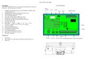
Setting and Connection<br />
Pull-out style<br />
TAG Panel<br />
Liftable cover<br />
System LED<br />
IO LED
After opening<br />
<strong>the</strong> cover<br />
DIP instruction<br />
Connection<br />
instruction<br />
Power<br />
ioSCADA - 23 - : 1.0<br />
SUNIX Co., Ltd.<br />
TEL : +886-2-8913-1987<br />
Email : info@sunix.com.tw<br />
Setting Baud Rate<br />
ioSCADA module has 4-PIN (SW-1’s 1~3,<strong>the</strong> fourth PIN is RTU/ASCII) ,through DIP switch can set o<strong>the</strong>r baud rate. Range:<br />
1200~11500 bps. Just like <strong>the</strong> images below, <strong>the</strong> value is set to baud rate 115200.<br />
The default factory baud rate is: 115200 bps<br />
Termianl<br />
Resistor<br />
IO<br />
Communication<br />
Baud Rate/RTU/ASCII<br />
Slave No./INIT<br />
Setting Slave No<br />
Before networking, checking <strong>the</strong> Slave No and baud rate’s DIP setting. The Slave No can’t be <strong>the</strong> same on one network. Each<br />
ioSCADA module has 7-PIN(SW-2’s1~6,<strong>the</strong> seventh PIN is INIT). Through DIP switch can set o<strong>the</strong>r Modbus Slave number,<br />
Fuse
ange: 1~63. Just like <strong>the</strong> images below, <strong>the</strong> value is set to NO.1。<br />
Slave NO calculation formula: NO = DIP1+DIP2*2+DIP3*4+DIP4*8+DIP5*16+DIP6*32<br />
ioSCADA - 24 - : 1.0<br />
SUNIX Co., Ltd.<br />
TEL : +886-2-8913-1987<br />
Email : info@sunix.com.tw<br />
Please every ioSCADA module on one RS-485 bus,make sure that <strong>the</strong>re is no same NO set to <strong>the</strong>m. If that happened, please<br />
adjust to avoid communication crash and data transfer failure caused by <strong>the</strong> modules.<br />
Protocol selection (RTU/ASCII)<br />
SW-1’s PIN4 can set to select Modbus RTU(OFF) or Modbus ASCII(ON)<br />
Reset Default Factiory Setting (INIT)<br />
The module function parameter can be reset to default factory setting by SW-2’s DIP7 switch,easy to maintain and inspection.<br />
Operaton order: 1. Cut-down <strong>the</strong> power supply<br />
2. Set DIP7 to ON<br />
3. Power supply on<br />
4. Set DIP back to OFF within 5 s( If failed to set DIP7 back to OFF within 5 s,do <strong>the</strong> whole process again)
ioSCADA - 25 - : 1.0<br />
SUNIX Co., Ltd.<br />
TEL : +886-2-8913-1987<br />
Email : info@sunix.com.tw<br />
Normal start LED display: After connect to Power supply : PWR bright、RX/TX flashes once,one second later,<br />
IO_ACC starts to flash after RX/TX flashs again<br />
INIT on start LED display: After connect to Power supply: PWR 亮、RX/TX flashes once,one second later, IO_ACC<br />
keeps bright after RX/TX flashes once again<br />
INIT off LED display: IO_ACC wink, 5 second later,IO_ACC starts to flash,system works normally<br />
Power Supply 、Communication Connection<br />
Basic install connection diagram:<br />
Normal Start System LED Display<br />
Cable mesh copper net<br />
After connect to Power supply : PWR bright、RX/TX flashes once,one second later,IO_ACC starts to flash after RX/TX flashes<br />
once again. When EEPROM value changed or failure, IO_ACC will slow down its flash speed.<br />
If RS485 terminal resistance has setting,Rt_ON will be bright.<br />
If RS485 is connected to <strong>the</strong> hose computer: RX is bright to display that <strong>the</strong> module has received <strong>the</strong> data, when TX is bright;<br />
it means <strong>the</strong> module has sent <strong>the</strong> data.<br />
When connected to <strong>the</strong> host computer,if RX flashes,TX doesn’t flash,<strong>the</strong> module ID address or baud rate maybe has a wrong<br />
setting.
Terminal Resistance( Rt)<br />
If ioSCADA is <strong>the</strong> terminal device of <strong>the</strong> RS-485 net, <strong>the</strong> Rt switch on <strong>the</strong> ioSCADA needs to be set ON<br />
PE<br />
ioSCADA - 26 - : 1.0<br />
SUNIX Co., Ltd.<br />
TEL : +886-2-8913-1987<br />
Email : info@sunix.com.tw<br />
PE is <strong>the</strong> most important in <strong>the</strong> ioSCADA system; PE offers <strong>the</strong> same reference point to <strong>the</strong> circuit, different device all needs to<br />
has its own PE stick. Such as computer system, power supply system, communication system, etc. RS-485’s COMMON point<br />
doesn't need to PE and <strong>the</strong> cable isolation net needs to PE with singl point.
Install Configure Software ioCFG<br />
ioSCADA - 27 - : 1.0<br />
SUNIX Co., Ltd.<br />
TEL : +886-2-8913-1987<br />
Email : info@sunix.com.tw<br />
ioCFG is <strong>the</strong> configure software which used to set different parameter of ioSCADA module, testing communication status and<br />
each channel connection situation. It’s free for users.<br />
Execute CD floder \ioCFG\Setup.exe to achieve installation.<br />
Caution:ioCFG.exe needs to work under Microsoft Windows .NET Framework 2.0 system or above, <strong>the</strong> install program will be<br />
recognized automatically and install itself.<br />
Execute ioCFG<br />
Execute ioCFG.exe application progame, after executing <strong>the</strong>re will be two windows coming out as following.<br />
Select RTU/ASCII: To make a choice of <strong>the</strong> communication protocol from <strong>the</strong> protocol hint window, you can choosed ei<strong>the</strong>r<br />
Modbus RTU or Modbus ASCII,Modbus TCP is now out of support. The module communication protocol can be set by DIP<br />
switch. The module won’t finish <strong>the</strong> connecton unless <strong>the</strong> protocol is chosen <strong>the</strong> same with <strong>the</strong> software.
COM and Baud Rate Selection:<br />
ioSCADA - 28 - : 1.0<br />
SUNIX Co., Ltd.<br />
TEL : +886-2-8913-1987<br />
Email : info@sunix.com.tw<br />
COM Port:: Select <strong>the</strong> COM of PC and ioSCADA<br />
Baud Rate: By <strong>the</strong> module DIP switch setting ,115200、57600、38400、19200、9600、4800、2400、1200 are available to<br />
be selected, or select <strong>the</strong> AUTO option to let software scan for you<br />
Lengh: The character length is 8 bit, choice disable<br />
Parity: None,choice disable<br />
Stop bit: 1,choice disable<br />
Timeout: The response from module to software is timeout, normal value is 100 ms,<strong>the</strong> longer time of timeout <strong>the</strong> longer<br />
time needed for scanning <strong>the</strong> 63 module.<br />
Delay between Poll: Set <strong>the</strong> delay time between two orders of <strong>the</strong> software,normal time would be 0 ms.
Autoscan screen: Communication parameter setting done,enter auto scan screen<br />
ioSCADA - 29 - : 1.0<br />
SUNIX Co., Ltd.<br />
TEL : +886-2-8913-1987<br />
Email : info@sunix.com.tw<br />
The autoscan can list <strong>the</strong> discovered module, such as 01-SM_DIO_116p VER:0.89, 01 is <strong>the</strong> module address, SM_DIO_116p<br />
is <strong>the</strong> module model, VER:0.89 is <strong>the</strong> firmware edition. If <strong>the</strong> module EEPROM is damaged, it will display <strong>the</strong> ERR code.<br />
Like <strong>the</strong> diagram 57-Scanning, it means that it has scanned 57 addresses at present, each station scaned once, it will start to scan<br />
<strong>the</strong> next station when timeout. The waiting time is like <strong>the</strong> timeout setting.<br />
It will wait for 3s before starting to scan from NODE 01.<br />
It will wait for 5s before starting to scan from NODE 01, if <strong>the</strong> screen changes back to scan diagram from <strong>the</strong> monitoring<br />
diagram. .<br />
Online/Offline Switch:<br />
Online can switch to Offline easily,it can do <strong>the</strong> offline edit during <strong>the</strong> Offline period, opening network or saving network,<br />
downloading and uploading datas.
Open Network: Reading module configure data,all <strong>the</strong> setting parameter of <strong>the</strong> network will be read<br />
Save Network: Saving <strong>the</strong> module parameter read online to files. One in network, on in every module.<br />
File name as: xxx.propect, xxx_ADDR_ID.module<br />
xxx: User save name<br />
XXX: User assigned Project file name<br />
ADDR: Module Slave NO<br />
ID: Module ID<br />
ioSCADA - 30 - : 1.0<br />
SUNIX Co., Ltd.<br />
TEL : +886-2-8913-1987<br />
Email : info@sunix.com.tw<br />
SM_AO_102(i) 327<br />
Attached file name.project saves <strong>the</strong> network configuration<br />
Attached file name.module saves <strong>the</strong> module configuration,each module has one, that be opened independently during module<br />
setting.<br />
Upload: Reading parameter data from module<br />
Download: Download all <strong>the</strong> network module data to module<br />
If switch to Online, all <strong>the</strong> offline data will lost.( Needing to remember to save <strong>the</strong> modified data)<br />
Module ID<br />
SM_DI_116p 297<br />
SM_DIO_116p 298<br />
SM_DO_108 299<br />
SM_DO_116 300<br />
SM_CNT_102 312<br />
SM_AI_108(i) 317<br />
SM_RTD_108(i) 317<br />
SM_TH_108(i) 317<br />
SM_UI_108(i) 317
Data Monitoring Overview Diagram<br />
Click <strong>the</strong> left-key of <strong>the</strong> mouse twice on <strong>the</strong> module scanned to enter <strong>the</strong> module setting diagram<br />
The screen will update by seconds,<strong>the</strong> real time curve section is 30s, <strong>the</strong> new data is on <strong>the</strong> right side.<br />
Whe choose Offline, <strong>the</strong> screen will stop update.<br />
DI Channel Parameter Setting<br />
Click DI0~DI7 to enter <strong>the</strong> DI channel setting diagram<br />
ioSCADA - 31 - : 1.0<br />
SUNIX Co., Ltd.<br />
TEL : +886-2-8913-1987<br />
Email : info@sunix.com.tw
ioSCADA - 32 - : 1.0<br />
SUNIX Co., Ltd.<br />
TEL : +886-2-8913-1987<br />
Email : info@sunix.com.tw<br />
The yellow field data can be modified and <strong>the</strong> green one can’t. The two colour can be exchanged under different mode.<br />
选The data selected to be modified will write into ioSCADA module directly,but it won’t save in EEPROM. It will come to<br />
defealt after power off. If you want it to change permanently, please click Save EEPROM.<br />
The number field instructions please take reference to Chapter 3 configuration setting.
DO Channel Parameter Setting<br />
Click DO0~DO7 to enter into DO channel setting diagram<br />
ioSCADA - 33 - : 1.0<br />
SUNIX Co., Ltd.<br />
TEL : +886-2-8913-1987<br />
Email : info@sunix.com.tw<br />
Power On-TPC and Fail Safe-TPC Safe is <strong>the</strong> same value. Click Logic to set i2o’s logical control,Select at least one DI input.<br />
The number field instructions please take reference to Chapter 3 configuration setting<br />
All Parameter Setting<br />
Click All to enter all channel parameter<br />
setting diagram<br />
Any modified data doesn’t write into <strong>the</strong> module directly, it needs to be click “Download” to save <strong>the</strong> changes into module. It
will execute Save EEPROM after download automatically.<br />
modifiy",<strong>the</strong> "Arrow" symbol means "Already Finish"<br />
I2O_Map value is between 0 ~ 255 ,that means 8 DI channels, 3 = CH0 and CH1 are selected<br />
ioSCADA - 34 - : 1.0<br />
SUNIX Co., Ltd.<br />
TEL : +886-2-8913-1987<br />
Email : info@sunix.com.tw<br />
Attention to <strong>the</strong> left "Pencil" symbol , it expresses "Failed to<br />
Save File can save <strong>the</strong> present parameter,Open File can read old files,Upload can upload data from <strong>the</strong> module.( When entering<br />
All screen,it will upload once automatically, Execute upload after download to make sure whe<strong>the</strong>r <strong>the</strong> download is<br />
successful) .<br />
File name is XXX.module.<br />
XXX is assigned file name by user.<br />
When execute Download,<strong>the</strong> modified data will be downloaded to <strong>the</strong> ioSCADA module, and save into EEPROM, it needs to<br />
wait 5 s to continue to do later operation.
Function block Timing Diagram<br />
SM_DI_116p、SM_DIO_116p<br />
ioSCADA - 35 - : 1.0<br />
SUNIX Co., Ltd.<br />
TEL : +886-2-8913-1987<br />
Email : info@sunix.com.tw<br />
Debounce : Filter nose, Only <strong>the</strong> on scene signal should keep <strong>the</strong> Debounce in <strong>the</strong> shortest time,<strong>the</strong> changed status can be confirmed. DI-in<br />
is <strong>the</strong> signal detected on scene; DI is <strong>the</strong> cognizance value of <strong>the</strong> module. If Debounce is set to be 100ms and one pulse is<br />
50ms,this pulse won’t be reveived. The pulse which is over 100ms can be received. The status read out is later than <strong>the</strong> actual<br />
by <strong>the</strong> Debounce time.<br />
Invert : Invert,to take <strong>the</strong> on scene signal as opposite,if <strong>the</strong> present singal is TRUE,<strong>the</strong> module will think it is FALSE,<br />
whereas,if <strong>the</strong> present signal is FALSE,<strong>the</strong> module will think it is TRUE. This is used for <strong>the</strong> normal open or normal<br />
close device junction adjustment.
ioSCADA - 36 - : 1.0<br />
SUNIX Co., Ltd.<br />
TEL : +886-2-8913-1987<br />
Email : info@sunix.com.tw<br />
On Delay / Off Delay: ON delay and OFF delay,you can choose one or both simultaneously of <strong>the</strong>m. The status recognized<br />
by <strong>the</strong> module will be later about a period set time than <strong>the</strong> realy present signal. The red line is <strong>the</strong> delay<br />
time set before, its unit is second.<br />
Toggle: Touched off by <strong>the</strong> detection upper, when <strong>the</strong> present signal changes from 0 to 1, <strong>the</strong> module status changes once, if it is OFF, it<br />
changeds to 1(ON),if it is ON, it changes to 0 (OFF).<br />
Pulse: Creating pulse signal, when <strong>the</strong> present signal changes from 0(OFF) to 1(ON), <strong>the</strong> module creats one fix baud pulse.<br />
If <strong>the</strong> present signal is always keeping 1(ON) status, it will change to 0(OFF) after.<br />
One Shot: Same as Pulse to produce pulse, but if <strong>the</strong> last springed pulse isn’t finish, <strong>the</strong> present signal springs again, <strong>the</strong> pulse<br />
time will count again, continuing to extend <strong>the</strong> pulse<br />
baud.
SM_DO_108、SM_DO_116、SM_DIO_116p<br />
ioSCADA - 37 - : 1.0<br />
SUNIX Co., Ltd.<br />
TEL : +886-2-8913-1987<br />
Email : info@sunix.com.tw<br />
Debounce: Filter nose, Only <strong>the</strong> on scene signal should keep <strong>the</strong> Debounce in <strong>the</strong> shortest time,<strong>the</strong> changed status can be confirmed. DO<br />
is <strong>the</strong> output order, Feedback is <strong>the</strong> module actual output status. If Debounce is set to be 100ms,DO order which<br />
wants to be confirmed needs to exceed 100ms.<br />
Invert : Invert,to take <strong>the</strong> on scene signal as opposite,if <strong>the</strong> present singal is TRUE,<strong>the</strong> module will think it is FALSE,<br />
whereas,if <strong>the</strong> present signal is FALSE,<strong>the</strong> module will think it is TRUE.
ioSCADA - 38 - : 1.0<br />
SUNIX Co., Ltd.<br />
TEL : +886-2-8913-1987<br />
Email : info@sunix.com.tw<br />
Delay: ON delay and OFF delay,you can choose one or both simultaneously of <strong>the</strong>m. The status recognized by <strong>the</strong><br />
module will be later about a period set time than <strong>the</strong> realy present signal. The red line is <strong>the</strong> delay time set before, its unit<br />
is second.<br />
Toggle: Touched off by <strong>the</strong> detection upper, when <strong>the</strong> present signal changes from 0 to 1, <strong>the</strong> module status changes once, if it is OFF, it<br />
changeds to 1(ON),if it is ON, it changes to 0 (OFF).<br />
Pulse: Creating pulse signal, when <strong>the</strong> present signal changes from 0(OFF) to 1(ON), <strong>the</strong> module creats one fix baud<br />
pulse. If <strong>the</strong> present signal is always keeping 1(ON) status, it will change to 0(OFF) after.<br />
One Shot: Same as Pulse to produce pulse, but if <strong>the</strong> last springed pulse isn’t finish, <strong>the</strong> present signal springs again, <strong>the</strong> pulse
time will count again, continuing to extend <strong>the</strong> pulse baud.<br />
ioSCADA - 39 - : 1.0<br />
SUNIX Co., Ltd.<br />
TEL : +886-2-8913-1987<br />
Email : info@sunix.com.tw<br />
Pulse & Clear: Just like Pulse, but when actual pulse turns to be 0(OFF) after finishing output,it will clear <strong>the</strong> order (DO) to<br />
0 (OFF) itself.<br />
One Shot & Clear: Same as One Shot, but when <strong>the</strong> actual pulse turns to be 0(OFF) after finishing output,it will clear <strong>the</strong><br />
order (DO) to 0(OFF) itself.
SM_AI_108i、SM_UI_108i、SM_RTD_108i、SM_TH_108i<br />
Smooth:<br />
<strong>Form</strong>ula: Y0 = (Y-X)/S + X<br />
Y0 : Present adjust value<br />
Y : Present value<br />
X : Previous value<br />
S : Smooth set value, when S=1, Smooth is ineffective.<br />
ioSCADA - 40 - : 1.0<br />
SUNIX Co., Ltd.<br />
TEL : +886-2-8913-1987<br />
Email : info@sunix.com.tw
Overflow alarm set value:<br />
SM_RTD_108i<br />
SM_UI_108i<br />
SM_TH_108i<br />
ioSCADA - 41 - : 1.0<br />
SUNIX Co., Ltd.<br />
TEL : +886-2-8913-1987<br />
Email : info@sunix.com.tw<br />
Name Over Flow Over Range Under Range Under Flow<br />
Pt100(385) 870 850 -200 -220<br />
Pt100(3902) 870 850 -200 -220<br />
Pt100(3916) 870 850 -200 -220<br />
Pt100(392) 870 850 -200 -220<br />
Pt100(3926) 870 850 -200 -220<br />
Pt200(385) 870 850 -200 -220<br />
Pt500(385) 870 850 -200 -220<br />
Pt 1000 (375) 870 850 -200 -220<br />
Pt 1000 (385) 870 850 -200 -220<br />
Ni120(672) 280 260 -80 -100<br />
Cu50(427) 280 260 -100 -120<br />
Cu100(427) 280 260 -100 -120<br />
Name Over Flow Over Range Under Range Under Flow<br />
+-100mV 32600 32000 -32000 -36000<br />
+-500mV 32600 32000 -32000 -36000<br />
+-5V 32600 32000 -32000 -36000<br />
+-10V 32600 32000 -32000 -36000<br />
1~5 V 32600 32000<br />
+-20mA 32600 32000 -32000 -36000<br />
4~20mA 32600 32000<br />
B 1840 1820 -260 240<br />
E 1020 1000 -200 -220<br />
J 1220 1200 -210 -230<br />
K 1392 1372 -200 -220<br />
N 1300 1320 -230 -250<br />
R 1788 1768 -50 -70<br />
S 1788 1768 -50 -70<br />
T 420 400 -260 -280<br />
Name Over Flow Over Range Under Range Under Flow
SM_AI_108i<br />
10K(TypeII/Z) 150 140 -45 -55<br />
10K(TypeIII/S) 150 140 -45 -55<br />
ioSCADA - 42 - : 1.0<br />
SUNIX Co., Ltd.<br />
TEL : +886-2-8913-1987<br />
Email : info@sunix.com.tw<br />
Name Over Flow Over Range Under Range Under Flow<br />
+-5V 32600 32000 -32000 -36000<br />
+-10V 32600 32000 -32000 -36000<br />
1~5 V 32600 32000 -32000 -36000<br />
+-20mA 32600 32000 -32000 -36000<br />
4~20mA 32600 32000
SM_AO_102i<br />
Clamp: Set AO high clamp and low clamp can limit output value within <strong>the</strong> special range.<br />
ioSCADA - 43 - : 1.0<br />
SUNIX Co., Ltd.<br />
TEL : +886-2-8913-1987<br />
Email : info@sunix.com.tw<br />
Slop Time: Slop Time is to define <strong>the</strong> request time to reach <strong>the</strong> target value, such as setting Slop Time to 100s, when <strong>the</strong> output<br />
changes from 0 to 4000, it will increase 40 per second. Slop Time will be ineffective when it is 0. Any target value<br />
( output) changes will be count again according to <strong>the</strong> formula, <strong>the</strong> origin point will take <strong>the</strong> present output point.<br />
Just as last example when <strong>the</strong> output changes to 1000, <strong>the</strong> target value will change to 3000 again, and <strong>the</strong>n <strong>the</strong><br />
output increase amount will be 30 per second. The renew output time will change once per 0.01s.
SM_CNT_102<br />
ioSCADA - 44 - : 1.0<br />
SUNIX Co., Ltd.<br />
TEL : +886-2-8913-1987<br />
Email : info@sunix.com.tw<br />
Cyclic/High Trigger: It will start to count when input changes to true from false, when it reaches Max-Count Value, <strong>the</strong> cyclic<br />
will count from 1.<br />
Cyclic/Low Trigger: It will start to count when input changes to false from true, when it reaches Max-Count Value, <strong>the</strong> cyclic<br />
will count from 1.<br />
Stop/High Trigger: It will start to count when input changes to true from false, when it reaches Max-Count Value, it stops<br />
count.<br />
Stop/Low Trigger: It will start to count when input changes to false from true, when it reaches Max-Count Value, it stops<br />
count.<br />
Alarm: When setting <strong>the</strong> Alarm Mode, <strong>the</strong> Alarm will output by <strong>the</strong> relatively DO.
Chatper 3 Configuration<br />
ioSCADA - 45 - : 1.0<br />
SUNIX Co., Ltd.<br />
TEL : +886-2-8913-1987<br />
Email : info@sunix.com.tw<br />
ioSCADA ‘s <strong>the</strong> parameter setting needs according to <strong>the</strong> application requirement. Besides <strong>the</strong> ioCFG.exe supported by<br />
SUNIX,any software which supports Modbsu RTU or Modbus ASCII communication protocol can set <strong>the</strong> module paremeter<br />
according to <strong>the</strong> Modbus address of <strong>the</strong> ioSCADA.<br />
Modbus Register Map<br />
Modbus’s internal data is divided into four kinds (0x、1x、3x、4x), <strong>the</strong> address is consist of two part, <strong>the</strong> first code can be 0、<br />
1、3、4, which is representative different internal block,<strong>the</strong> second part x can be 1~65535 according to different RAM size of<br />
different device,usually using three-code 01~999、four-code 001~9999 or five-code 001~99999 to display. ioSCADA can use<br />
four or five code address format.( It will be 5 or 6 code including <strong>the</strong> first code.)<br />
<strong>Address</strong> Instructions<br />
0x Write and read digital output Coil,bit data. Any 0x’s address can be both read and written, usually it is digital<br />
output or internal parameter<br />
1x Read only digital input state,bit data. Any 1x’s address can’t be written. Error code usually is digital state<br />
point.<br />
3x Read only analog input register, integer data. Any 3x’s address can’t be written,Error code usually is analog<br />
value point.<br />
4x Read and write hold register, integer data. Any 4x’s address can be both write and read, usually it is analog<br />
output or internal value parameter.<br />
Cautions:<br />
1. "x" expresses 1~65536,base-16 0~FFFF( 在传送命令时address 40001 will be divided into function code3 and address 0) .<br />
The first code of <strong>the</strong> Modbus protocol is hidden order function code, <strong>the</strong> last five is <strong>the</strong> actual address of different RAM. If<br />
<strong>the</strong> first code is 0 or 1, it means Bit region,its state is ei<strong>the</strong>r 0 or 1、16 Bit address form one word. If <strong>the</strong> first code is 3 or 4,<br />
it means WORD region. ioSCADA is used 4-in-1 register map design,0、1、3、4 four kinds of RAM region are actual<br />
homologous to one place. That means no matter what <strong>the</strong> first code is, it will be read out <strong>the</strong> same data if only <strong>the</strong> last four or<br />
five code assigned address is <strong>the</strong> same (<strong>the</strong> last five code of 0、1 divding 16 will come out <strong>the</strong> 3、4 Word address). Such as<br />
00001~00016(Bit) = 10001~10016(Bit) = 30001(Word) = 40001(Word)<br />
ioSCADA Modbus address:<br />
ioSACAD address is divided into two kinds, one is present data address which starts from1 (40001),<strong>the</strong> o<strong>the</strong>r is module<br />
parameter which stars from 9001(49001). The present data is created by <strong>the</strong> operation, it will loss when power off. The module<br />
parameter will be read from EEPROM when it starts operation. It can be read or modified during operation, also it can be set to<br />
read only, <strong>the</strong> modified parameter can be saved back to EEPROM according to <strong>the</strong> special steps, it will be saved into EEPROM
when power off.<br />
SM_DIO_116p - DI Data Process Diagram<br />
SM_DIO_116p - DO Data Process Diagram<br />
<strong>Address</strong> <strong>Index</strong> <strong>Following</strong> <strong>the</strong> <strong>Form</strong> <strong>Number</strong><br />
SM_DIO_116p Present Data<br />
ioSCADA - 46 - : 1.0<br />
SUNIX Co., Ltd.<br />
TEL : +886-2-8913-1987<br />
Email : info@sunix.com.tw<br />
NO. <strong>Address</strong> Instruction Data <strong>Form</strong>at Unit
1 00001~00008 (RO)<br />
10001~10008 (RO)<br />
30001 (RO)<br />
40001 (RO)<br />
2 0017~0024 (RW)<br />
10017~10024 (RO)<br />
30002 (RO)<br />
40002 (RW)<br />
3 00033~00040 (RO)<br />
10033~10040 (RO)<br />
30003 (RO)<br />
40003 (RO)<br />
4 00049~00056 (RO)<br />
10049~10056 (RO)<br />
30004 (RO)<br />
40004 (RO)<br />
5 00065~00072 (RO)<br />
10065~10072 (RO)<br />
30005 (RO)<br />
40005 (RO)<br />
6 00081~00088 (RO)<br />
10081~10088 (RO)<br />
30006 (RO)<br />
40006 (RO)<br />
7 30009 ~ 30016 (RO)<br />
40009 ~ 40016 (RO)<br />
8 30017 ~ 30024 (RW)<br />
40017 ~ 40024 (RW)<br />
9 00385 ~ 00040 (RW)<br />
10385 ~ 10040 (RO)<br />
30025 (RO)<br />
40025 (RW)<br />
10 00401 ~ 00416 (RW)<br />
10401 ~ 10416 (RO)<br />
30026 (RO)<br />
40026 (RW)<br />
ioSCADA - 47 - : 1.0<br />
SUNIX Co., Ltd.<br />
TEL : +886-2-8913-1987<br />
Email : info@sunix.com.tw<br />
DI0 ~ DI7 Status Digital input,occupying 8 bit of <strong>the</strong>16 bit<br />
Word( Low Byte), 1 is True (ON),0 is False<br />
(OFF)。<br />
10009 ~ 10016 meaningless,value=0<br />
The status is <strong>the</strong> value dealt with by <strong>the</strong><br />
signal process function block. Just like <strong>the</strong><br />
data process diagram display.<br />
DO0 ~ DO7 Output Digital output,occupying 8 bit of <strong>the</strong> 16 bit<br />
Word( Low Byte), 1 isTrue (ON),0 is False<br />
(OFF)。<br />
00025 ~ 00032 meaningless,value=0<br />
forvever<br />
DI0 ~ DI7 On Latch<br />
Status<br />
When DI Status changes to 1 from 0, DI On<br />
Latch Status is set to 1,Reset to clear to 0.<br />
DI0 ~ DI7 Off Latch Status When DI Status changes to 0 from 1,DI<br />
Off Latch Status is set to1,Reset to clear to 0. Bit<br />
DI0 ~ DI7 DI-in DI Status’s original data,coming directly<br />
from <strong>the</strong> hardware, hasn’t been processed by<br />
<strong>the</strong> function block.<br />
DO0 ~ DO7 Output<br />
Feedback Status<br />
Bit<br />
Bit<br />
Bit<br />
Bit<br />
DO actual output status feedback Bit<br />
0/1<br />
DI0 ~ DI7 Count Value DI Status’s count value,when DI Status<br />
changes to 1 from 0, <strong>the</strong> present value adds 1.<br />
It has <strong>the</strong> count function,only when <strong>the</strong><br />
Counter Active’s parameter is 1(Enable)<br />
When in <strong>the</strong> Simulatiopn Mode, <strong>the</strong> value<br />
can be wiritten in by <strong>the</strong> master.<br />
DO0 ~ DO7 TCP Output Used when <strong>the</strong> mode isTPC, toge<strong>the</strong>r with<br />
Duty Cycle can be changed to DO junction<br />
output by 0~100%.<br />
DI0 ~ DI7 Bypass<br />
DO0 ~ DO7 Manual<br />
DI0 ~ DI7 Simulation<br />
DO0 ~ DO7 Simulation<br />
40025 low byte 00385 ~ 00392 为DI0 ~ DI7<br />
Set Bypass<br />
1 = Bypass ,0 = Normal<br />
40025 high byte 00393 ~ 00040 为<br />
DO0~DO7 Set Manual<br />
1 = Manual ,0 = Manual<br />
40026 low byte 00401 ~ 00408 为DI0 ~ DI7<br />
Simulation<br />
40026 high byte 00409 ~ 00416 为DO0 ~<br />
DO7 Simulation<br />
1 = Simulation,0 = Normal<br />
WORD<br />
0~65535<br />
%<br />
0 ~ 100<br />
Bit<br />
Bit
11 00417 ~ 00424 (RW)<br />
10417 ~ 10424 (RO)<br />
30027 (RO)<br />
40027 (RW)<br />
12 00433 ~ 00440 (RW)<br />
10433 ~ 10440 (RO)<br />
30028 (RO)<br />
40028 (RW)<br />
DI0 ~ DI7 Latch Clear<br />
DI0 ~ DI7 Count Clear<br />
ioSCADA - 48 - : 1.0<br />
SUNIX Co., Ltd.<br />
TEL : +886-2-8913-1987<br />
Email : info@sunix.com.tw<br />
Let DI On Latch/Off Latch Status reset to 0<br />
1 = Clear,reset to 0(5s later)<br />
Let DI Count value reset to 0,when <strong>the</strong> Flag<br />
changes to 1 from 0,it’s active, and reset to 0<br />
after 5s .<br />
Bit<br />
Bit
SM_DIO_116p Module Parameter<br />
ioSCADA - 49 - : 1.0<br />
SUNIX Co., Ltd.<br />
TEL : +886-2-8913-1987<br />
Email : info@sunix.com.tw<br />
NO. <strong>Address</strong> Instruction Data Fomat Unit<br />
21 39001 (RO)<br />
49001 (RO)<br />
22 39002 (RO)<br />
49002 (RO)<br />
23 39003 (RO)<br />
49003 (RO)<br />
24 39005 (RO)<br />
49005 (RW)<br />
25 39006 (RO)<br />
49006 (RW)<br />
26 39007 (RO)<br />
49007 (RW)<br />
27 39009 (RO)<br />
49009 (RW)<br />
28 39010 (RO)<br />
49010 (RW)<br />
Product ID<br />
Module ID<br />
SM_DI_116p 297<br />
SM_DIO_116p 298<br />
SM_DO_108 299<br />
SM_DO_116 300<br />
SM_CNT_102 312<br />
SM_AI_108(i) 317<br />
SM_RTD_108(i) 318<br />
SM_TH_108(i) 319<br />
SM_UI_108(i) 320<br />
SM_AO_102(i) 327<br />
Product Version 100 = 1.00,<strong>the</strong> dual ending number is <strong>the</strong> formal version,<br />
<strong>the</strong> single ending number is <strong>the</strong> test version<br />
System error 0 = OK<br />
1 = Flash Read Error (If error stil after reboot,needing<br />
repairation)<br />
2 = Flash checksum Error ( expresses <strong>the</strong> set value or <strong>the</strong><br />
calibration is broken, needing to reset)<br />
Cation: The Flash may fail to be writen into but can be<br />
read, <strong>the</strong> system can’t judge this kind of error.<br />
Configuration Setup Set to 0,disable to modify any setting parameter.Set to 1.<br />
Able t be modified by Master, Set to 7 from 1, <strong>the</strong> data<br />
will be saved into EEPROM. When saving into<br />
EEPROM,<strong>the</strong> module will recover to work after 5s.<br />
During this time all function is disable.<br />
Reboot to go back to get default value 1<br />
Modbus Exception 0 = Command Exception Disable<br />
1 = Command Exception Enable<br />
Response Delay Time Sometime Master needs <strong>the</strong> slave delay a certain time to<br />
reply after get <strong>the</strong> order. The immediate respond will<br />
cause <strong>the</strong> <strong>the</strong> cmmunication errors.<br />
DI0 ~ DI7 Invert<br />
DO0 ~ DO7 Invert<br />
DI0 ~ DI7 Read<br />
Latch Clear<br />
Let actual DI input status input reversely or let DO order<br />
output reversely.<br />
Low Byte = DI0 ~ DI7 Invert<br />
High Byte = DO0 ~ DO7 Invert<br />
1=Invert,0=Normal<br />
After master read DI On/Off Status, it reset to 0, avoid<br />
reading <strong>the</strong> repetitive alarm data .<br />
Low Byte = DI0 ~ DI7 Read Latch Clear<br />
High Byte = Always 0<br />
1 = Clear,0 = Normal<br />
WORD<br />
WORD<br />
WORD<br />
WROD<br />
WORD<br />
ms<br />
0~65535<br />
Bit<br />
Bit
29 39011 (RO)<br />
49011 (RW)<br />
30 39012 (RO)<br />
49012 (RW)<br />
31 39013 (RO)<br />
49013 (RW)<br />
32 39014 (RO)<br />
49014 (RW)<br />
33 39016 (RO)<br />
49016 (RW)<br />
34 39017~39024(RO)<br />
49017~49024(RW)<br />
35 39025~39032(RO)<br />
49025~49032(RW)<br />
36 39033~39040(RO)<br />
49033~49040(RW)<br />
37 39041~39048(RO)<br />
49041~49048(RW)<br />
DI0 ~ DI7 Counter<br />
Enable<br />
DO0~DO7 i2o<br />
DO0 ~ DO7 Power<br />
On<br />
& i2o logic<br />
DO0 ~ DO7 Fail<br />
Latch<br />
Set to 1 to enable <strong>the</strong> count function<br />
Low Byte = DI0 ~ DI7 Counter Enable<br />
High Byte = DO0~DO7 input to output<br />
1 = i2o,0 = Normal<br />
ioSCADA - 50 - : 1.0<br />
SUNIX Co., Ltd.<br />
TEL : +886-2-8913-1987<br />
Email : info@sunix.com.tw<br />
On power,DO’s output value, ineffective in TPC mode.<br />
Low Byte = DO0 ~ DO7 Power On<br />
1 = On,0 = Off<br />
High Byte = DO0~DO7 i2o (AND/OR) logic<br />
0 = AND, 1=OR<br />
When communication watchdog is active, sing poion is<br />
ineffective, that means it will keep <strong>the</strong> original state<br />
when communication failure.<br />
Low Byte = DO0 ~ DO7 Fail Latch<br />
High Byte = Always 0<br />
1 = Latch,0 = Fail Safe<br />
DO0 ~ DO7 Fail Safe When watch dog detects communication broken, it is<br />
enforced to output ON or Off<br />
1 = On,0 = Off<br />
Low Byte = DO0 ~ DO7 Fail Safe<br />
High Byte = Always 0<br />
Fail Time The time of watch dog, 0 is Fail Safe Disable. All DO<br />
share one set value.<br />
DI0~DI7 Signal<br />
Processing Mode<br />
DO0~DO7 Signal<br />
Processing Mode<br />
0 = Direct<br />
1 = Delayed<br />
2 = Toggled<br />
3 = Pulsed<br />
4 = One Shot<br />
0 = Direct<br />
1 = Delayed<br />
2 = Toggled<br />
3 = Pulsed<br />
4 = One Shot 5 =<br />
Pulsed&Clear<br />
6 = One Shot&Clear<br />
7 = TPC<br />
DI0~DI7 Debounce Confirm <strong>the</strong> input status changed after input signal keeps<br />
a certain time.<br />
DO0~DO7 Debounce Confirm <strong>the</strong> output status changed after output signal<br />
keeps a certain time.<br />
Bit<br />
Bit<br />
Bit<br />
Bit<br />
ms<br />
0~65535<br />
WORD<br />
0~4<br />
WORD<br />
0~7<br />
5ms<br />
0~65535<br />
5ms<br />
0~65535
38 39049~39056(RO)<br />
49049~49056(RW)<br />
39 39057~39064(RO)<br />
49057~49064(RW)<br />
40 39065~39072(RO)<br />
49065~49072(RW)<br />
41 39073~39080(RO)<br />
49073~49080(RW)<br />
42 39081~39088(RO)<br />
49081~49088(RW)<br />
43 39097~390104(RO)<br />
49097~490104(RW)<br />
44 39113~39120(RO)<br />
49113~49120(RW)<br />
DI0~DI7 On Delay<br />
Time<br />
DO0~DO7 On Delay<br />
Time<br />
DI0~DI7 Off Delay<br />
Time/Pulse Time<br />
DO0~DO7 Off Delay<br />
Time/Pulse Time<br />
DO0~DO7 TPC Duty<br />
Cycle Time<br />
DO0~DO7 TPC Fail<br />
Safe/Power On<br />
Output<br />
DO0~DO7 i2o logic<br />
pattern select<br />
ioSCADA - 51 - : 1.0<br />
SUNIX Co., Ltd.<br />
TEL : +886-2-8913-1987<br />
Email : info@sunix.com.tw<br />
DI status changes to on from off, delay time s<br />
0~65535<br />
DO order changes to on from off, delay time s<br />
0~65535<br />
DI status changes to off from on, delay time or Pulse<br />
Mode’s Pulse baud<br />
DO order changes to off from on, delay time or Pulse<br />
Mode’s Pulse baud<br />
s<br />
0~65535<br />
s<br />
0~65535<br />
Do in TPC Mode,TPC duty cycle time. 0.1 s<br />
0~3000<br />
Do in TPC Mode,TPC output percent or <strong>the</strong> safe value of<br />
<strong>the</strong> communication error. If not set Fail Time,output<br />
will be 0% by power on.<br />
Using Low Byte 8 bit to express DI0~DI7<br />
0 = not selected; 1 = selected<br />
%<br />
0~100<br />
bit
SM_DI_116p Data Process Diagram<br />
ioSCADA - 52 - : 1.0<br />
SUNIX Co., Ltd.<br />
TEL : +886-2-8913-1987<br />
Email : info@sunix.com.tw
<strong>Address</strong> <strong>Index</strong> <strong>Following</strong> <strong>the</strong> <strong>Form</strong> <strong>Number</strong><br />
SM_DI_116p Present Data<br />
ioSCADA - 53 - : 1.0<br />
SUNIX Co., Ltd.<br />
TEL : +886-2-8913-1987<br />
Email : info@sunix.com.tw<br />
NO. <strong>Address</strong> Instruction Data Fomat Unit<br />
1 00001~00016 (RO)<br />
10001~10016 (RO)<br />
30001 (RO)<br />
40001 (RO)<br />
2 00017~00032 (RW)<br />
10017~10032 (RO)<br />
30002 (RO)<br />
40002 (RO)<br />
3 00033~00048 (RO)<br />
10033~10048 (RO)<br />
30003 (RO)<br />
40003 (RO)<br />
4 00049~00064 (RO)<br />
10049~10064 (RO)<br />
30004 (RO)<br />
40004 (RO)<br />
5 30009 ~30024 (RO)<br />
40009 ~ 400024 (RO)<br />
6 00385 ~ 00040 (RW)<br />
10385 ~ 10040 (RO)<br />
30025 (RO)<br />
40025 (RW)<br />
7 00401 ~ 00416 (RW)<br />
10401 ~ 10416 (RO)<br />
30026 (RO)<br />
40026 (RW)<br />
8 00417 ~ 00432 (RW)<br />
10417 ~ 10432 (RO)<br />
30027 (RO)<br />
40027 (RW)<br />
9 00433 ~ 00448 (RW)<br />
10433 ~ 10448 (RO)<br />
30028 (RO)<br />
40028 (RW)<br />
DI0 ~ DI15 Status Digtal input,occupying 8 bit of <strong>the</strong> 16 bit Word( Low Byte),<br />
1 is True (ON),0 isFalse (OFF)。<br />
The status is <strong>the</strong> value dealt with by <strong>the</strong> signal process<br />
function block. Just like <strong>the</strong> data process diagram display.<br />
DI0 ~ DI15 On<br />
Latch Status<br />
DI0 ~ DI15 Off<br />
Latch Status<br />
When DI Status changes to 1 from 0, DI On Latch Status<br />
will be set to 1,Reset to clear to 0.<br />
When DI Status changes to 0 from 1, DI Off Latch Status<br />
will be set to 1,Reset to clear to 0.<br />
DI0 ~ DI15 DI - in DI Status’s original data,directly value which comes from<br />
<strong>the</strong> hardware, hasn’t been dealt with by <strong>the</strong> function block.<br />
DI0 ~ DI15Count<br />
Value<br />
DI0 ~ DI15 Bypass<br />
DI0 ~ DI15<br />
Simulation<br />
DI0 ~ DI15 Latch<br />
Clear<br />
DI0 ~ DI15 Count<br />
Clear<br />
DI Status’s count value, when DI Status changes to 1 from 0,<br />
<strong>the</strong> present value adds 1. When Counter Active’s parameter<br />
is 1 , <strong>the</strong> count function is enable.<br />
In Simulatiopn Mode,this value can be input by <strong>the</strong> Master.<br />
00385 ~ 0040 为DI0 ~ DI15 Bypass<br />
1 = Bypass,0 = Normal<br />
00401 ~ 00416 为DI0 ~ DI15 Simulation<br />
1 = Simulation,0 = Normal<br />
Let DI On Latch/Off Latch Status reset to 0<br />
1 = Reset,reset to 0 after 5s itself.<br />
Let DI Count value reset to 0. It will be active when Flag<br />
changes to 1 from 0,and it will reset to 0 after 5s itself.<br />
Bit<br />
Bit<br />
Bit<br />
Bit<br />
WORD<br />
0~65535<br />
Bit<br />
Bit<br />
Bit<br />
Bit
SM_DI_116p Module Parameter<br />
ioSCADA - 54 - : 1.0<br />
SUNIX Co., Ltd.<br />
TEL : +886-2-8913-1987<br />
Email : info@sunix.com.tw<br />
NO. <strong>Address</strong> Instruction Data Fomat Unit<br />
21 39001 (RO)<br />
49001 (RO)<br />
22 39002 (RO)<br />
49002 (RO)<br />
23 39003 (RO)<br />
49003 (RO)<br />
24 39005 (RO)<br />
49005 (RW)<br />
25 39006 (RO)<br />
49006 (RW)<br />
26 39007 (RO)<br />
49007 (RW)<br />
27 39009 (RO)<br />
49009 (RW)<br />
28 39010 (RO)<br />
49010 (RW)<br />
Product ID<br />
Module ID<br />
SM_DI_116p 297<br />
SM_DIO_116p 298<br />
SM_DO_108 299<br />
SM_DO_116 300<br />
SM_CNT_102 312<br />
SM_AI_108(i) 317<br />
SM_RTD_108(i) 318<br />
SM_TH_108(i) 319<br />
SM_UI_108(i) 320<br />
SM_AO_102(i) 327<br />
Product Version 100 = 1.00, <strong>the</strong> dual ending number is <strong>the</strong> formal<br />
version, <strong>the</strong> single ending number is <strong>the</strong> test version<br />
System error 0 = OK<br />
1 = Flash Read Error (If error still after reboot,needing<br />
repairation)<br />
2 = Flash checksum Error ( expresses <strong>the</strong> set value or <strong>the</strong><br />
calibration is broken, needing to reset)<br />
Cation: The Flash may fail to be writen into but can be<br />
read, <strong>the</strong> system can’t judge this kind of error.<br />
Configuration Setup Set to 0,disable to modify any setting parameter . Set to<br />
1. Able t be modified by Master, Set to 7 from 1, <strong>the</strong> data<br />
will be saved into EEPROM. When saving into<br />
EEPROM,<strong>the</strong> module will recover to work after 5s.<br />
During this time all function is disable.<br />
Reboot to go back to get default value 1<br />
Modbus Exception 0 = Command Exception Disable<br />
1 = Command Exception Enable<br />
Response Delay Time Sometime Master needs <strong>the</strong> slave delay a certain time to<br />
reply after get <strong>the</strong> order. The immediate respond will<br />
cause <strong>the</strong> <strong>the</strong> cmmunication errors.<br />
DI0 ~ DI15 Invert<br />
DI0 ~ DI15 Read<br />
Latch Clear<br />
Let actual DI input status input reversely , Low Byte =<br />
DI0 ~ DI7 Invert, High Byte = DI8 ~ DI15 Invert<br />
After master read DI On/Off Status, it reset to 0, avoid<br />
reading <strong>the</strong> repetitive alarm data.<br />
1 = Read Clear,0 = Normal<br />
WORD<br />
WORD<br />
WORD<br />
WROD<br />
WORD<br />
ms<br />
0~6553<br />
5<br />
Bit<br />
Bit
29 39011 (RO)<br />
49011 (RW)<br />
30 39017~39032(RO)<br />
49017~49032(RW)<br />
31 39033~39048(RO)<br />
49033~49048(RW)<br />
32 39049~39064(RO)<br />
49049~49064(RW)<br />
33 39065~39080(RO)<br />
49065~49080(RW)<br />
DI0 ~ DI15 Counter<br />
Enable<br />
DI0~DI15 Signal<br />
Processing Mode<br />
ioSCADA - 55 - : 1.0<br />
SUNIX Co., Ltd.<br />
TEL : +886-2-8913-1987<br />
Email : info@sunix.com.tw<br />
设定为1 时才对有 计 数 功能 Bit<br />
0 = Direct<br />
1 = Delayed<br />
2 = Toggled<br />
3 = Pulsed<br />
4 = One Shot<br />
DI0~DI15 Debounce Confirm <strong>the</strong> input status changed after input signal keeps<br />
a certain time.<br />
DI0~DI15<br />
On Delay Time<br />
DI0~DI15 Off Delay<br />
Time/Pulse Time<br />
WORD<br />
0~4<br />
5ms<br />
0~6553<br />
5<br />
DI status changes to on from off, delay time s<br />
0~6553<br />
5<br />
DI status changes to off from on, delay time or Pulse<br />
Mode’s Pulse baud<br />
s<br />
0~6553<br />
5
SM_DO_116、SM_DO_108 Data Process Diagram<br />
ioSCADA - 56 - : 1.0<br />
SUNIX Co., Ltd.<br />
TEL : +886-2-8913-1987<br />
Email : info@sunix.com.tw
<strong>Address</strong> <strong>Index</strong> <strong>Following</strong> <strong>the</strong> <strong>Form</strong> <strong>Number</strong><br />
SM_DO_116 Present Data<br />
ioSCADA - 57 - : 1.0<br />
SUNIX Co., Ltd.<br />
TEL : +886-2-8913-1987<br />
Email : info@sunix.com.tw<br />
NO. <strong>Address</strong> Instruction Data Fomat Unit<br />
1 00001~00016 (RW)<br />
10001~10016 (RO)<br />
30001 (RO)<br />
40001 (RW)<br />
2 00017~00032 (RO)<br />
10017~10032 (RO)<br />
30002 (RO)<br />
40002 (RO)<br />
3 30009 ~ 30024 (RW)<br />
40009 ~ 40024 (RW)<br />
4 00385 ~ 00400 (RW)<br />
10385 ~ 10400 (RO)<br />
30025 (RO)<br />
40025 (RW)<br />
5 00401 ~ 00416 (RW)<br />
10401 ~ 10416 (RO)<br />
30026 (RO)<br />
40026 (RW)<br />
DO0 ~ DO15<br />
Output<br />
DO0 ~ DO15<br />
Output Feedback<br />
Status<br />
DO0 ~ DO15 TCP<br />
Output<br />
DO0 ~ DO15<br />
Manual<br />
DO0 ~ DO15<br />
Simulation<br />
Digital output, occupying 16 bit Word, 1 is True (ON),0 is<br />
False (OFF)。<br />
DO actual output status feedback Bit<br />
Used when <strong>the</strong> Mode isTPC,toge<strong>the</strong>r with Duty Cycle can be<br />
changed to DO junction output by 0~100%.<br />
DO0 ~ DO15 Manual<br />
1 = Manual,0 = Normal<br />
DO0 ~ DO15 Simulation<br />
1 = Simulation,0 = Normal<br />
Bit<br />
%<br />
0 ~ 100<br />
Bit<br />
Bit
SM_DO_116 Module Parameter<br />
ioSCADA - 58 - : 1.0<br />
SUNIX Co., Ltd.<br />
TEL : +886-2-8913-1987<br />
Email : info@sunix.com.tw<br />
NO. <strong>Address</strong> Instruction Data Fomat Unit<br />
21 39001 (RO)<br />
49001 (RO)<br />
22 39002 (RO)<br />
49002 (RO)<br />
23 39003 (RO)<br />
49003 (RO)<br />
24 39005 (RO)<br />
49005 (RW)<br />
25 39006 (RO)<br />
49006 (RW)<br />
26 39007 (RO)<br />
49007 (RW)<br />
27 39009 (RO)<br />
49009 (RW)<br />
28 39012 (RO)<br />
49012 (RW)<br />
Product ID<br />
Module ID<br />
SM_DI_116p 297<br />
SM_DIO_116p 298<br />
SM_DO_108 299<br />
SM_DO_116 300<br />
SM_CNT_102 312<br />
SM_AI_108(i) 317<br />
SM_RTD_108(i) 318<br />
SM_TH_108(i) 319<br />
SM_UI_108(i) 320<br />
SM_AO_102(i) 327<br />
Product Version 100 = 1.00,<strong>the</strong> dual ending number is <strong>the</strong> formal version,<br />
<strong>the</strong> single ending number is <strong>the</strong> test version<br />
System error 0 = OK<br />
1 = Flash Read Error (If error still after reboot,needing<br />
repairation)<br />
2 = Flash checksum Error ( expresses <strong>the</strong> set value or <strong>the</strong><br />
calibration is broken, needing to reset)<br />
Cation: The Flash may fail to be writen into but can be<br />
read, <strong>the</strong> system can’t judge this kind of error.<br />
Configuration Setup Set to 0,disable to modify any setting parameter. Set to 1.<br />
Able t be modified by Master, Set to 7 from 1, <strong>the</strong> data<br />
will be saved into EEPROM. When saving into<br />
EEPROM,<strong>the</strong> module will recover to work after 5s.<br />
During this time all function is disable.<br />
Reboot to go back to get default value 1<br />
Modbus Exception 0 = Command Exception Disable<br />
1 = Command Exception Enable<br />
Response Delay Time Sometime Master needs <strong>the</strong> slave delay a certain time to<br />
reply after get <strong>the</strong> order. The immediate respond will<br />
cause <strong>the</strong> <strong>the</strong> cmmunication errors.<br />
DO0 ~ DO15 Invert Let DO order output reversely<br />
Low Byte = DO0 ~ DO7 Invert<br />
High Byte = DO8 ~ DO15 Invert<br />
1 = Invert,0 = Normal<br />
DO0 ~ DO15 Power<br />
On<br />
On power,DO’s output value, ineffective in TPC mode. 1<br />
= On,0 = Off<br />
Low Byte = DO0 ~ DO7 Power On<br />
High Byte = DO8 ~ DO15 Power On<br />
WORD<br />
WORD<br />
WORD<br />
WROD<br />
WORD<br />
ms<br />
0~65535<br />
Bit<br />
Bit
29 39013 (RO)<br />
49013 (RW)<br />
30 39014 (RO)<br />
49014 (RW)<br />
31 39016 (RO)<br />
49016 (RW)<br />
32 39017~39032(RO)<br />
49017~49032(RW)<br />
33 39033~39048(RO)<br />
49033~49040(RW)<br />
34 39049~39064(RO)<br />
49049~49064(RW)<br />
35 39065~39080(RO)<br />
49065~49080(RW)<br />
36 39081~39096(RO)<br />
49081~49096(RW)<br />
37 39097~390112(RO)<br />
49097~490112(RW)<br />
DO0 ~ DO15 Fail<br />
Latch<br />
DO0 ~ DO15 Fail<br />
Safe<br />
ioSCADA - 59 - : 1.0<br />
SUNIX Co., Ltd.<br />
TEL : +886-2-8913-1987<br />
Email : info@sunix.com.tw<br />
When communication watchdog is active, sing poion is<br />
ineffective, that means it will keep <strong>the</strong> original state when<br />
communication failure.<br />
Low Byte = DO0 ~ DO7 Fail Latch<br />
High Byte = DO8 ~ DO15 Fail Latch<br />
1 = Latch,0 = Fail Safe<br />
When watch dog detects communication broken, it is<br />
enforced to output ON or Off<br />
Low Byte = DO0 ~ DO7 Fail Safe<br />
High Byte = DO8 ~ DO15 Fail Safe<br />
1 = On,0 = Off<br />
Fail Time 通讯Watch Dog 的时间,0 表示Fail Safe Disable。全部DO<br />
共享一个设定值。<br />
DO0~DO15 Signal<br />
Processing Mode<br />
DO0~DO15<br />
Debounce<br />
DO0~DO15 On<br />
Delay Time<br />
DO0~DO15 Off<br />
Delay Time/Pulse<br />
Time<br />
DO0~DO15 TPC<br />
Duty Cycle Time<br />
DO0~DO16 TPC Fail<br />
Safe/Power On<br />
Output<br />
0 = Direct<br />
1 = Delayed<br />
2 = Toggled<br />
3 = Pulsed<br />
4 = One Shot 5 =<br />
Pulsed&Clear<br />
6 = One Shot&Clear<br />
7 = TPC<br />
49017 = DO0 Mode 依次 49018=DO1 Mode<br />
Confirm <strong>the</strong> output status changed after output signal<br />
keeps a certain time<br />
49033 = DO0 Debounce 49034=DO1 Debounce<br />
DO order changes to on from off, delay time.<br />
49049 = DO0 On Delay Time<br />
DO order changes to off from on, delay time or Pulse<br />
Mode’s Pulse baud<br />
49065 = DO0 Off Delay Time<br />
Do in TPC Mode,TPC duty cycle time.<br />
49081 = DO0 Duty Cycle Time<br />
Do in TPC Mode,TPC outputs percent or <strong>the</strong> safe value<br />
of <strong>the</strong> communication error. If not set Fail Time,output<br />
will be 0% by power on.<br />
Fail Safe and Power On share <strong>the</strong> same parameter<br />
49097 = DO0 Fail Safe/Power On Output<br />
Bit<br />
Bit<br />
s<br />
0~65535<br />
WORD<br />
0~7<br />
5ms<br />
0~65535<br />
s<br />
0~65535<br />
s<br />
0~65535<br />
0.1 s<br />
1~3000<br />
%<br />
0~100
SM_DO_108 Present Data<br />
ioSCADA - 60 - : 1.0<br />
SUNIX Co., Ltd.<br />
TEL : +886-2-8913-1987<br />
Email : info@sunix.com.tw<br />
NO. <strong>Address</strong> Instruction Data Fomat Unit<br />
1 00001~00008 (RW)<br />
10001~10008 (RO)<br />
30001 (RO)<br />
40001 (RW)<br />
2 00017~00024 (RO)<br />
10017~10024 (RO)<br />
30002 (RO)<br />
40002 (RO)<br />
3 30009 ~ 30016 (RW)<br />
40009 ~ 40016 (RW)<br />
4 00385 ~ 00392 (RW)<br />
10385 ~ 10392 (RO)<br />
30025 (RO)<br />
40025 (RW)<br />
5 00401 ~ 00408 (RW)<br />
10401 ~ 10408 (RO)<br />
30026 (RO)<br />
40026 (RW)<br />
DO0 ~ DO7 Output Digital output,occupying 8 bit of <strong>the</strong> 16 bit Word 中的8 位<br />
( Low Byte), 1 is True (ON),0 is False (OFF)。<br />
DO0 ~ DO7 Output<br />
Feedback Status<br />
DO0 ~ DO7 TCP<br />
Output<br />
DO actual output status feedback Bit<br />
Used when <strong>the</strong> mode isTPC, toge<strong>the</strong>r with Duty Cycle can be<br />
changed to DO junction output by 0~100%.<br />
DO0 ~ DO7 Manual DO0 ~ DO7 Manual<br />
1 = Manual,0 = Normal<br />
DO0 ~ DO7<br />
Simulation<br />
DO0 ~ DO7 Simulation<br />
1 = Simulation,0 = Normal<br />
Bit<br />
%<br />
0 ~ 100<br />
Bit<br />
Bit
SM_DO_108 Module Parameter<br />
ioSCADA - 61 - : 1.0<br />
SUNIX Co., Ltd.<br />
TEL : +886-2-8913-1987<br />
Email : info@sunix.com.tw<br />
NO. <strong>Address</strong> Instruction Data Fomat Unit<br />
21 39001 (RO)<br />
49001 (RO)<br />
22 39002 (RO)<br />
49002 (RO)<br />
23 39003 (RO)<br />
49003 (RO)<br />
24 39005 (RO)<br />
49005 (RW)<br />
25 39006 (RO)<br />
49006 (RW)<br />
26 39007 (RO)<br />
49007 (RW)<br />
27 39009 (RO)<br />
49009 (RW)<br />
28 39012 (RO)<br />
49012 (RW)<br />
Product ID<br />
Module ID<br />
SM_DI_116p 297<br />
SM_DIO_116p 298<br />
SM_DO_108 299<br />
SM_DO_116 300<br />
SM_CNT_102 312<br />
SM_AI_108(i) 317<br />
SM_RTD_108(i) 318<br />
SM_TH_108(i) 319<br />
SM_UI_108(i) 320<br />
SM_AO_102(i) 327<br />
Product Version 100 = 1.00,<strong>the</strong> dual ending number is <strong>the</strong> formal version,<br />
<strong>the</strong> single ending number is <strong>the</strong> test version<br />
System error 0 = OK<br />
1 = Flash Read Error (If error still after reboot,needing<br />
repairation)<br />
2 = Flash checksum Error ( expresses <strong>the</strong> set value or <strong>the</strong><br />
calibration is broken, needing to reset)<br />
Cation: The Flash may fail to be writen into but can be<br />
read, <strong>the</strong> system can’t judge this kind of error.<br />
Configuration Setup Set to 0,disable to modify any setting parameter. Set to 1.<br />
Able t be modified by Master, Set to 7 from 1, <strong>the</strong> data<br />
will be saved into EEPROM. When saving into<br />
EEPROM,<strong>the</strong> module will recover to work after 5s.<br />
During this time all function is disable.<br />
Reboot to go back to get default value 1<br />
Modbus Exception 0 = Command Exception Disable<br />
1 = Command Exception Enable<br />
Response Delay Time Sometime Master needs <strong>the</strong> slave delay a certain time to<br />
reply after get <strong>the</strong> order. The immediate respond will<br />
cause <strong>the</strong> <strong>the</strong> cmmunication errors.<br />
DO0 ~ DO7 Invert Let DO order output reversely<br />
Low Byte = DO0 ~ DO7 Invert<br />
High Byte = 0<br />
1 = Invert,0 = Normal<br />
DO0 ~ DO7 Power<br />
On<br />
On power,DO’s output value, ineffective in TPC mode.<br />
1 = On,0 = Off<br />
Low Byte = DO0 ~ DO7 Power On<br />
High Byte = 0<br />
WORD<br />
WORD<br />
WORD<br />
WROD<br />
WORD<br />
ms<br />
0~65535<br />
Bit<br />
Bit
29 39013 (RO)<br />
49013 (RW)<br />
30 39014 (RO)<br />
49014 (RW)<br />
31 39016 (RO)<br />
49016 (RW)<br />
32 39017~39024(RO)<br />
49017~49024(RW)<br />
33 39033~39040(RO)<br />
49033~49040(RW)<br />
34 39049~39056(RO)<br />
49049~49056(RW)<br />
35 39065~39072(RO)<br />
49065~49072(RW)<br />
36 39081~39088(RO)<br />
49081~49088(RW)<br />
37 39097~390104(RO)<br />
49097~490104(RW)<br />
DO0 ~ DO7 Fail<br />
Latch<br />
ioSCADA - 62 - : 1.0<br />
SUNIX Co., Ltd.<br />
TEL : +886-2-8913-1987<br />
Email : info@sunix.com.tw<br />
When communication watchdog is active, sing poion is<br />
ineffective, that means it will keep <strong>the</strong> original state<br />
when communication failure.<br />
Low Byte = DO0 ~ DO7 Fail Latch<br />
High Byte = 0<br />
1 = Latch,0 = Fail Safe<br />
DO0 ~ DO7 Fail Safe When watch dog detects communication broken, it is<br />
enforced to output ON or Off<br />
1 = On,0 = Off<br />
Low Byte = DO0 ~ DO7 Fail Safe<br />
High Byte = 0<br />
Fail Time The time of watch dog, 0 is Fail Safe Disable. All DO<br />
share one set value.<br />
DO0~DO7 Signal<br />
Processing Mode<br />
0 = Direct<br />
1 = Delayed<br />
2 = Toggled<br />
3 = Pulsed<br />
4 = One Shot 5 =<br />
Pulsed&Clear<br />
6 = One Shot&Clear<br />
7 = TPC<br />
49017 = DO0 Mode, 49018=DO1 Mode<br />
DO0~DO7 Debounce Confirm <strong>the</strong> output status changed after output signal<br />
keeps a certain time.<br />
49033 = DO0 Debounce,49034=DO1 Debounce<br />
DO0~DO7 On Delay<br />
Time<br />
DO0~DO7 Off Delay<br />
Time/Pulse Time<br />
DO0~DO7 TPC Duty<br />
Cycle Time<br />
DO0~DO7 TPC Fail<br />
Safe/Power On<br />
Output<br />
DO order changes to on from off, delay time<br />
49049 = DO0 On Delay Time<br />
DO order changes to off from on, delay time or Pulse<br />
Mode’s Pulse baud<br />
49065 = DO0 Off Delay Time<br />
Do in TPC Mode,TPC duty cycle time.<br />
49081 = DO0 Duty Cycle Time<br />
Do in TPC Mode,TPC outputs percent or <strong>the</strong> safe value<br />
of <strong>the</strong> communication error. If not set Fail Time,output<br />
will be 0% by power on.<br />
Fail Safe and Power On share on parameter.<br />
49097 = DO0 Fail Safe/Power On Output<br />
Bit<br />
Bit<br />
s<br />
0~65535<br />
WORD<br />
0~7<br />
5ms<br />
0~65535<br />
s<br />
0~65535<br />
s<br />
0~65535<br />
0.1 s<br />
1~3000<br />
%<br />
0~100
SM_AI_108i Data Process Diagram<br />
<strong>Address</strong> <strong>Index</strong> <strong>Following</strong> <strong>the</strong> <strong>Form</strong> <strong>Number</strong><br />
SM_AI_108i Present Data<br />
ioSCADA - 63 - : 1.0<br />
SUNIX Co., Ltd.<br />
TEL : +886-2-8913-1987<br />
Email : info@sunix.com.tw<br />
NO. <strong>Address</strong> Instruction Data Fomat Unit<br />
1 30001~ 30008(RO)<br />
40001~ 40008 (RO)<br />
2 00129 ~ 00256(RO)<br />
10129 ~ 10256(RO)<br />
30009 ~ 300016(RO)<br />
40009 ~ 40016(RO)<br />
3 30017 ~ 30024 (RW)<br />
40017 ~ 40024 (RW)<br />
4 30025 ~ 30032 (RW)<br />
40025 ~ 40032 (RW)<br />
AI0 ~ AI7 Value Normal Range is -3200 ~ 3200,<strong>the</strong> exceeded ones is Over<br />
Range, <strong>the</strong> one lower than -32768 or higher than 32767 is<br />
Over Flow<br />
AI0 ~ AI7 Status AI0 ~ AI7 Alarm status,each AI point take one WORD,it has<br />
7 kinds of status: 0 is OK,only takes BIT0 ~ BIT6,<strong>the</strong> o<strong>the</strong>r<br />
bit is 0<br />
After alarm, <strong>the</strong> manual operation is needed to clear <strong>the</strong> alarm<br />
status<br />
BIT0 = High Alarm<br />
BIT1 = Low Alarm<br />
BIT2 = Over Range ( > 3200 )<br />
BIT3 = Under Range ( < 3200)<br />
BIT4 = Over Flow ( > 3260 )<br />
BIT5 = Under Flow ( < 3260 )<br />
BIT6 = Break<br />
1~5V and 4~20 mA has no Under Range and Under Flow<br />
alarm.<br />
AI0 ~ AI7 Max<br />
Value<br />
AI0 ~ AI7 Min<br />
Value<br />
WORD<br />
±32768<br />
AI0 ~ AI7 moment Max value WORD<br />
AI0 ~ AI7 moment Min value WORD<br />
Bit
5 00513 ~ 00520 (RW)<br />
10513 ~ 10520 (RO)<br />
30033 (RO)<br />
40033 (RW)<br />
6 00529 ~ 00536 (RW)<br />
10529 ~ 10536 (RO)<br />
30034 (RO)<br />
40034 (RW)<br />
7 00545 ~ 00552 (RW)<br />
10545 ~ 10552 (RO)<br />
30026 (RO)<br />
40026 (RW)<br />
AI0 ~ AI7<br />
Simulation<br />
AI0 ~ AI7 Max/Min<br />
Reset<br />
AI0 ~ AI7 Alarm<br />
Reset<br />
SM_AI_108i Module Parameter<br />
ioSCADA - 64 - : 1.0<br />
SUNIX Co., Ltd.<br />
TEL : +886-2-8913-1987<br />
Email : info@sunix.com.tw<br />
AI0 ~ AI7 Simulation, <strong>the</strong> actual input will not update in <strong>the</strong><br />
Simulation mode, <strong>the</strong> value can be set by <strong>the</strong> Host<br />
40033 的High Byte 为0<br />
Let AI0 ~ AI7 Max/Min value reset and count again.<br />
40034’s High Byte 为0<br />
Let AI0 ~ AI7’s alarm status be cleared<br />
40035’s High Byte 为0<br />
NO. <strong>Address</strong> Instruction Data Fomat Unit<br />
21 39001 (RO)<br />
49001 (RO)<br />
22 39002 (RO)<br />
49002 (RO)<br />
Product ID<br />
Module ID<br />
SM_DI_116p 297<br />
SM_DIO_116p 298<br />
SM_DO_108 299<br />
SM_DO_116 300<br />
SM_CNT_102 312<br />
SM_AI_108(i) 317<br />
SM_RTD_108(i) 318<br />
SM_TH_108(i) 319<br />
SM_UI_108(i) 320<br />
SM_AO_102(i) 327<br />
Product Version 100 = 1.00, <strong>the</strong> dual ending number is <strong>the</strong> formal<br />
version, <strong>the</strong> single ending number is <strong>the</strong> test version.<br />
Bit<br />
Bit<br />
Bit<br />
WORD<br />
WORD
23 39003 (RO)<br />
49003 (RO)<br />
24 39005 (RO)<br />
49005 (RW)<br />
25 39006 (RO)<br />
49006 (RW)<br />
26 39007 (RO)<br />
49007 (RW)<br />
27 39017~39024(RO)<br />
49017~49024(RW)<br />
28 39025~39032(RO)<br />
49025~49032(RW)<br />
29 39033~39040(RO)<br />
49033~49040(RW)<br />
90 39041~39048(RO)<br />
49041~49048(RW)<br />
31 39049~39056(RO)<br />
49049~49056(RW)<br />
ioSCADA - 65 - : 1.0<br />
SUNIX Co., Ltd.<br />
TEL : +886-2-8913-1987<br />
Email : info@sunix.com.tw<br />
System error 0 = OK<br />
1 = Flash Read Error (If error still after reboot,needing<br />
repairation)<br />
2 = Flash checksum Error ( expresses <strong>the</strong> set value or <strong>the</strong><br />
calibration is broken, needing to reset)<br />
Cation: The Flash may fail to be writen into but can be<br />
read, <strong>the</strong> system can’t judge this kind of error.<br />
Configuration Setup Set to 0,disable to modify any setting parameter. Set to 1.<br />
Able t be modified by Master, Set to 7 from 1, <strong>the</strong> data<br />
will be saved into EEPROM. When saving into<br />
EEPROM,<strong>the</strong> module will recover to work after 5s.<br />
During this time all function is disable.<br />
Reboot to go back to get default value 1<br />
Modbus Exception 0 = Command Exception Disable<br />
1 = Command Exception Enable<br />
Response Delay Time Sometime Master needs <strong>the</strong> slave delay a certain time to<br />
reply after get <strong>the</strong> order. The immediate respond will<br />
cause <strong>the</strong> <strong>the</strong> cmmunication errors.<br />
AI0~AI7 Signal Type<br />
Type Name<br />
7 +-5V<br />
8 +-10V<br />
9 1~5V<br />
20 +-20mA<br />
22 4~20mA<br />
AI0~AI7 Offset Measure accroding to <strong>the</strong> instrument offset value,offset<br />
range is -128 ~ 127<br />
AI0~AI7 Smooth <strong>Form</strong>ula: O=X+(Y-X)/S<br />
O=Smooth value after calculation<br />
Y=present input value<br />
X=previous calculated value<br />
S=Smooth value,S=1 ( ineffective)<br />
AI0~AI7 High<br />
Alarm<br />
AI0~AI7 LOW<br />
Alarm<br />
WORD<br />
WROD<br />
WORD<br />
ms<br />
0~65535<br />
WORD<br />
0~7<br />
WORD<br />
WORD<br />
1~255<br />
High alarm setting WORD<br />
±3200<br />
Low alarm setting WORD<br />
±3200
SM_RTD_108i Data Process Diagram<br />
<strong>Address</strong> <strong>Index</strong> <strong>Following</strong> <strong>the</strong> <strong>Form</strong> <strong>Number</strong><br />
SM_RTD_108i Present Data<br />
ioSCADA - 66 - : 1.0<br />
SUNIX Co., Ltd.<br />
TEL : +886-2-8913-1987<br />
Email : info@sunix.com.tw<br />
NO. <strong>Address</strong> Instruction Data Fomat Unit<br />
1 309001 ~30008(RO)<br />
40001~ 40008 (RO)<br />
2 00129 ~ 00256(RO)<br />
10129 ~ 102556(RO)<br />
30009 ~ 30016(RO)<br />
40009 ~ 40016(RO)<br />
3 30017 ~ 30024 (RW)<br />
40017 ~ 40024 (RW)<br />
4 30025 ~ 30032 (RW)<br />
40025 ~ 40032 (RW)<br />
RTD0 ~ RTD7<br />
Value<br />
RTD0 ~ RTD7<br />
Status<br />
RTD0 ~ RTD7 Max<br />
Value<br />
RTD0 ~ RTD7 Min<br />
Value<br />
量测值 为 温 度单位( 0.1 or 0.1 ) 0.1<br />
±32768<br />
RTD0 ~ RTD7 警 报 状 态,每一RTD 点占用一个WORD,有七种<br />
状态: 0 表示OK,只用到BIT0 ~ BIT6,其他位为0<br />
警报消失后, 必须手动复归才可清除警 报 状 态<br />
BIT0 = High Alarm<br />
BIT1 = Low Alarm<br />
BIT2 = Over Range<br />
BIT3 = Under Range<br />
BIT4 = Over Flow<br />
BIT5 = Under Flow<br />
BIT6 = Break<br />
RTD0 ~ RTD7 瞬间最大值 WORD<br />
RTD0 ~ RTD7 瞬间最小值 WORD<br />
Bit
5 00513 ~ 00520 (RW)<br />
10513 ~ 10520 (RO)<br />
30033 (RO)<br />
40033 (RW)<br />
6 00529 ~ 00536 (RW)<br />
10529 ~ 10536 (RO)<br />
30034 (RO)<br />
40034 (RW)<br />
7 00545 ~ 00552 (RW)<br />
10545 ~ 10552 (RO)<br />
30026 (RO)<br />
40026 (RW)<br />
RTD0 ~ RTD7<br />
Simulation<br />
RTD0 ~ RTD7<br />
Max/Min Reset<br />
RTD0 ~ RTD7<br />
Alarm Reset<br />
ioSCADA - 67 - : 1.0<br />
SUNIX Co., Ltd.<br />
TEL : +886-2-8913-1987<br />
Email : info@sunix.com.tw<br />
RTD0 ~ RTD7 Simulation,Simulation mode 时实际输入不再更<br />
新, 数 值 可以由 Host 设定<br />
40033 的High Byte 为0<br />
将RTD0 ~ RTD7 Max/Min 数 值 复 归重新计算<br />
40034 的High Byte 为0<br />
将RTD0 ~ RTD7 的Alarm 状态清除<br />
40035 的High Byte 为0<br />
Bit<br />
Bit<br />
Bit
SM_RTD_108i Module Parameter<br />
ioSCADA - 68 - : 1.0<br />
SUNIX Co., Ltd.<br />
TEL : +886-2-8913-1987<br />
Email : info@sunix.com.tw<br />
NO. <strong>Address</strong> Instruction Data Fomat Unit<br />
21 39001 (RO)<br />
49001 (RO)<br />
22 39002 (RO)<br />
49002 (RO)<br />
23 39003 (RO)<br />
49003 (RO)<br />
24 39005 (RO)<br />
49005 (RW)<br />
25 39006 (RO)<br />
49006 (RW)<br />
26 39007 (RO)<br />
49007 (RW)<br />
27 90010 (RO)<br />
49010 (RW)<br />
Product ID<br />
Module ID<br />
SM_DI_116p 297<br />
SM_DIO_116p 298<br />
SM_DO_108 299<br />
SM_DO_116 300<br />
SM_CNT_102 312<br />
SM_AI_108(i) 317<br />
SM_RTD_108(i) 318<br />
SM_TH_108(i) 319<br />
SM_UI_108(i) 320<br />
SM_AO_102(i) 327<br />
Product Version 100 = 1.00, <strong>the</strong> dual ending number is <strong>the</strong> formal version,<br />
<strong>the</strong> single ending number is <strong>the</strong> test version.<br />
System error 0 = OK<br />
1 = Flash Read Error (If error still after reboot,needing<br />
repairation)<br />
2 = Flash checksum Error ( expresses <strong>the</strong> set value or <strong>the</strong><br />
calibration is broken, needing to reset)<br />
Cation: The Flash may fail to be writen into but can be<br />
read, <strong>the</strong> system can’t judge this kind of error.<br />
Configuration Setup Set to 0,disable to modify any setting parameter. Set to 1.<br />
Able t be modified by Master, Set to 7 from 1, <strong>the</strong> data<br />
will be saved into EEPROM. When saving into<br />
EEPROM,<strong>the</strong> module will recover to work after 5s.<br />
During this time all function is disable.<br />
Reboot to go back to get default value 1<br />
Modbus Exception 0 = Command Exception Disable<br />
1 = Command Exception Enable<br />
Response Delay Time Sometime Master needs <strong>the</strong> slave delay a certain time to<br />
reply after get <strong>the</strong> order. The immediate respond will<br />
cause <strong>the</strong> <strong>the</strong> cmmunication errors.<br />
Temperature Unit 使用的温度单位<br />
0 =<br />
1 =<br />
WORD<br />
WORD<br />
WORD<br />
WROD<br />
WORD<br />
ms<br />
0~65535
28 39017~39024(RO)<br />
49017~49024(RW)<br />
29 39025~39032(RO)<br />
49025~49032(RW)<br />
30 39033~39040(RO)<br />
49033~49040(RW)<br />
31 39041~39048(RO)<br />
49041~49048(RW)<br />
32 39049~39056(RO)<br />
49049~49056(RW)<br />
RTD0~RTD7 Signal<br />
Type<br />
Type Name<br />
61 Pt100(385)<br />
62 Pt100(3902)<br />
63 Pt100(3916)<br />
64 Pt100(392)<br />
65 Pt100(3926)<br />
71 Pt200(385)<br />
81 Pt500(385)<br />
90 Pt 1000 (375)<br />
91 Pt 1000 (385)<br />
101 Ni120(672)<br />
105 Cu50(427)<br />
110 Cu100(427)<br />
ioSCADA - 69 - : 1.0<br />
SUNIX Co., Ltd.<br />
TEL : +886-2-8913-1987<br />
Email : info@sunix.com.tw<br />
RTD0~RTD7 Offset Measure accroding to <strong>the</strong> instrument offset value,offset<br />
range is -128 ~ 127<br />
RTD0~RTD7<br />
Smooth<br />
RTD0~RTD7 High<br />
Alarm<br />
RTD0~RTD7 LOW<br />
Alarm<br />
<strong>Form</strong>ula: O=X+(Y-X)/S<br />
O=Smooth value after calculation<br />
Y=present input value<br />
X=previous calculated value<br />
S=Smooth value,S=1 ( ineffective)<br />
WORD<br />
WORD<br />
WORD<br />
1~255<br />
High alarm setting WORD<br />
±3200<br />
Low alarm setting WORD<br />
±3200
SM_TH_108i Data Process Diagram<br />
ioSCADA - 70 - : 1.0<br />
SUNIX Co., Ltd.<br />
TEL : +886-2-8913-1987<br />
Email : info@sunix.com.tw
<strong>Address</strong> <strong>Index</strong> <strong>Following</strong> <strong>the</strong> <strong>Form</strong> <strong>Number</strong><br />
SM_TH_108i Present Data<br />
ioSCADA - 71 - : 1.0<br />
SUNIX Co., Ltd.<br />
TEL : +886-2-8913-1987<br />
Email : info@sunix.com.tw<br />
NO. <strong>Address</strong> Instruction Data Fomat Unit<br />
1 30001 ~30008(RO)<br />
40001~ 40008 (RO)<br />
2 00129 ~ 00256(RO)<br />
10129 ~ 10256(RO)<br />
30009 ~ 30016(RO)<br />
40009 ~ 40016(RO)<br />
3 30017 ~ 30024 (RW)<br />
30017 ~ 30024 (RW)<br />
4 30025 ~ 30032 (RW)<br />
40025 ~ 40032 (RW)<br />
5 00513 ~ 00520 (RW)<br />
10513 ~ 10520 (RO)<br />
30033 (RO)<br />
40033 (RW)<br />
6 00529 ~ 00536 (RW)<br />
10529 ~ 10536 (RO)<br />
30034 (RO)<br />
40034 (RW)<br />
7 00545 ~ 00552 (RW)<br />
10545 ~ 10552 (RO)<br />
30026 (RO)<br />
40026 (RW)<br />
TH0 ~ TH7 Value The measure value is <strong>the</strong> temperature unit( 0.1 or 0.1 )<br />
TH0 ~ TH7 Status TH0 ~ TH7 alarm status, each TH point takes a WORD.<br />
it has 7 kinds of status: 0 is OK,only takes BIT0 ~ BIT6,<strong>the</strong><br />
o<strong>the</strong>r bit is 0<br />
After alarm, <strong>the</strong> manual operation is needed to clear <strong>the</strong> alarm<br />
status<br />
BIT0 = High Alarm<br />
BIT1 = Low Alarm<br />
BIT2 = Over Range<br />
BIT3 = Under Range<br />
BIT4 = Over Flow<br />
BIT5 = Under Flow<br />
BIT6 = Break<br />
TH0 ~ TH7 Max<br />
Value<br />
TH0 ~ TH7 Min<br />
Value<br />
TH0 ~ TH7<br />
Simulation<br />
TH0 ~ TH7<br />
Max/Min Reset<br />
TH0 ~ TH7 Alarm<br />
Reset<br />
SM_TH_108i Module Parameter<br />
0.1<br />
±32768<br />
TH0 ~ TH7 moment Max value WORD<br />
TH0 ~ TH7 moment Min value WORD<br />
TH0 ~ TH7 Simulation,<strong>the</strong> actual input will not update in <strong>the</strong><br />
Simulation mode, <strong>the</strong> value can be set by <strong>the</strong> Host.<br />
40033 的High Byte 为0<br />
Let TH0 ~ TH7 Max/Min value reset and count again.<br />
40034 的High Byte 为0<br />
Let TH0 ~ TH7’s alarm status be cleared<br />
40035 的High Byte 为0<br />
NO. <strong>Address</strong> Instruction Data Fomat Unit<br />
Bit<br />
Bit<br />
Bit<br />
Bit
21 39001 (RO)<br />
49001 (RO)<br />
22 39002 (RO)<br />
49002 (RO)<br />
23 39003 (RO)<br />
49003 (RO)<br />
24 39005 (RO)<br />
49005 (RW)<br />
25 39006 (RO)<br />
49006 (RW)<br />
26 39007 (RO)<br />
49007 (RW)<br />
27 90010 (RO)<br />
49010 (RW)<br />
28 39017~39024(RO)<br />
49017~49024(RW)<br />
29 39025~39032(RO)<br />
49025~49032(RW)<br />
Product ID<br />
Module ID<br />
SM_DI_116p 297<br />
SM_DIO_116p 298<br />
SM_DO_108 299<br />
SM_DO_116 300<br />
SM_CNT_102 312<br />
SM_AI_108(i) 317<br />
SM_RTD_108(i) 318<br />
SM_TH_108(i) 319<br />
SM_UI_108(i) 320<br />
SM_AO_102(i) 327<br />
ioSCADA - 72 - : 1.0<br />
SUNIX Co., Ltd.<br />
TEL : +886-2-8913-1987<br />
Email : info@sunix.com.tw<br />
Product Version 100 = 1.00,<strong>the</strong> dual ending number is <strong>the</strong> formal version,<br />
<strong>the</strong> single ending number is <strong>the</strong> test version.<br />
System error 0 = OK<br />
1 = Flash Read Error (If error still after reboot,needing<br />
repairation)<br />
2 = Flash checksum Error ( expresses <strong>the</strong> set value or <strong>the</strong><br />
calibration is broken, needing to reset)<br />
Cation: The Flash may fail to be writen into but can be<br />
read, <strong>the</strong> system can’t judge this kind of error.<br />
Configuration Setup Set to 0,disable to modify any setting parameter. Set to 1.<br />
Able t be modified by Master, Set to 7 from 1, <strong>the</strong> data<br />
will be saved into EEPROM. When saving into<br />
EEPROM,<strong>the</strong> module will recover to work after 5s.<br />
During this time all function is disable.<br />
Reboot to go back to get default value 1<br />
Modbus Exception 0 = Command Exception Disable<br />
1 = Command Exception Enable<br />
Response Delay Time Sometime Master needs <strong>the</strong> slave delay a certain time to<br />
reply after get <strong>the</strong> order. The immediate respond will<br />
cause <strong>the</strong> <strong>the</strong> cmmunication errors.<br />
Temperature Unit Used temperature unit<br />
0 =<br />
1 =<br />
TH0~TH7 Signal<br />
Type<br />
Type Name<br />
50 10K ( TypeII/Z )<br />
51 10K ( TypeIII/Z )<br />
TH0~TH7 Offset Measure accroding to <strong>the</strong> instrument offset value,offset<br />
range is -128 ~ 127<br />
WORD<br />
WORD<br />
WORD<br />
WROD<br />
WORD<br />
ms<br />
0~65535<br />
WORD<br />
WORD
30 39033~39040(RO)<br />
49033~49040(RW)<br />
31 39041~39048(RO)<br />
49041~49048(RW)<br />
32 39049~39056(RO)<br />
49049~49056(RW)<br />
TH0~TH7 Smooth <strong>Form</strong>ula : O=X+(Y-X)/S<br />
O=Smooth value after calculation<br />
Y= present input value<br />
X= previous calculated value<br />
S=Smooth value,S=1 ( ineffective)<br />
TH0~TH7 High<br />
Alarm<br />
TH0~TH7 LOW<br />
Alarm<br />
ioSCADA - 73 - : 1.0<br />
SUNIX Co., Ltd.<br />
TEL : +886-2-8913-1987<br />
Email : info@sunix.com.tw<br />
WORD<br />
1~255<br />
High alarm setting WORD<br />
±3200<br />
Low alarm setting WORD<br />
±3200
SM_UI_108i Data Process Diagram<br />
<strong>Address</strong> <strong>Index</strong> <strong>Following</strong> <strong>the</strong> <strong>Form</strong> <strong>Number</strong><br />
SM_UI_108i Present Data<br />
ioSCADA - 74 - : 1.0<br />
SUNIX Co., Ltd.<br />
TEL : +886-2-8913-1987<br />
Email : info@sunix.com.tw<br />
NO. <strong>Address</strong> Instruction Data Fomat Unit<br />
1 30001 ~30008(RO)<br />
40001~ 40008 (RO)<br />
2 00129 ~ 00256(RO)<br />
10129 ~ 10256(RO)<br />
30009 ~ 30016(RO)<br />
40009 ~ 40016(RO)<br />
3 30017 ~ 30024 (RW)<br />
40017 ~ 40024 (RW)<br />
UI0 ~ UI7 Value mV、mA、V normal range is -3200 ~ 3200, <strong>the</strong> exceeded ones<br />
is Over Range,<strong>the</strong> one lower than -32768 or higher than<br />
32767 is Over Flow<br />
T/C ‘s measure value is temperature unit( 0.1 or 0.1 )<br />
UI0 ~ UI7 Status UI0 ~ UI7 alarm status,each UI ake one WORD,it has 7<br />
kinds of status: 0 is OK,only takes BIT0 ~ BIT6,<strong>the</strong> o<strong>the</strong>r bit<br />
is 0<br />
After alarm, <strong>the</strong> manual operation is needed to clear <strong>the</strong> alarm<br />
status<br />
BIT0 = High Alarm<br />
BIT1 = Low Alarm<br />
BIT2 = Over Range<br />
BIT3 = Under Range<br />
BIT4 = Over Flow<br />
BIT5 = Under Flow<br />
BIT6 = Break<br />
UI0 ~ UI7 Max<br />
Value<br />
0.1<br />
±32768<br />
UI0 ~ UI7 moment Max value WORD<br />
Bit
4 30025 ~ 30032 (RW)<br />
40025 ~ 40032 (RW)<br />
5 00513 ~ 00520 (RW)<br />
10513 ~ 10520 (RO)<br />
30033 (RO)<br />
40033 (RW)<br />
6 00529 ~ 00536 (RW)<br />
10529 ~ 10536 (RO)<br />
30034 (RO)<br />
40034 (RW)<br />
7 00545 ~ 00552 (RW)<br />
10545 ~ 10552 (RO)<br />
30026 (RO)<br />
40026 (RW)<br />
UI0 ~ UI7 Min<br />
Value<br />
UI0 ~ UI7<br />
Simulation<br />
UI0 ~ UI7 Max/Min<br />
Reset<br />
UI0 ~ UI7 Alarm<br />
Reset<br />
SM_UI_108i Module Parameter<br />
ioSCADA - 75 - : 1.0<br />
SUNIX Co., Ltd.<br />
TEL : +886-2-8913-1987<br />
Email : info@sunix.com.tw<br />
UI0 ~ UI7 moment Min value WORD<br />
UI0 ~ UI7 Simulation,<strong>the</strong> actual input will not update in <strong>the</strong><br />
Simulation mode, <strong>the</strong> value can be set by <strong>the</strong> Host<br />
40033 的High Byte 为0<br />
Let UI0 ~ UI7 Max/Min value reset and count again.<br />
40034 的High Byte 为0<br />
Let UI0 ~ UI7 ‘s alarm status to be cleared<br />
40035 的High Byte 为0<br />
NO. <strong>Address</strong> Instruction Data Fomat Unit<br />
21 39001 (RO)<br />
49001 (RO)<br />
22 39002 (RO)<br />
49002 (RO)<br />
23 39003 (RO)<br />
49003 (RO)<br />
Product ID<br />
Module ID<br />
SM_DI_116p 297<br />
SM_DIO_116p 298<br />
SM_DO_108 299<br />
SM_DO_116 300<br />
SM_CNT_102 312<br />
SM_AI_108(i) 317<br />
SM_RTD_108(i) 318<br />
SM_TH_108(i) 319<br />
SM_UI_108(i) 320<br />
SM_AO_102(i) 327<br />
Product Version 100 = 1.00,<strong>the</strong> dual ending number is <strong>the</strong> formal version, <strong>the</strong><br />
single ending number is <strong>the</strong> test version.<br />
System error 0 = OK<br />
1 = Flash Read Error (If error still after reboot,needing<br />
repairation)<br />
2 = Flash checksum Error ( expresses <strong>the</strong> set value or <strong>the</strong><br />
calibration is broken, needing to reset)<br />
Cation: The Flash may fail to be writen into but can be read,<br />
<strong>the</strong> system can’t judge this kind of error.<br />
Bit<br />
Bit<br />
Bit<br />
WORD<br />
WORD<br />
WORD
24 39005 (RO)<br />
49005 (RW)<br />
25 39006 (RO)<br />
49006 (RW)<br />
26 39007 (RO)<br />
49007 (RW)<br />
27 90010 (RO)<br />
49010 (RW)<br />
28 90010 (RO)<br />
49010 (RW)<br />
29 39017~39024(RO)<br />
49017~49024(RW)<br />
30 39025~39032(RO)<br />
49025~49032(RW)<br />
31 39033~39040(RO)<br />
49033~49040(RW)<br />
ioSCADA - 76 - : 1.0<br />
SUNIX Co., Ltd.<br />
TEL : +886-2-8913-1987<br />
Email : info@sunix.com.tw<br />
Configuration Setup Set to 0,disable to modify any setting parameter. Set to 1.<br />
Able t be modified by Master, Set to 7 from 1, <strong>the</strong> data will<br />
be saved into EEPROM. When saving into EEPROM,<strong>the</strong><br />
module will recover to work after 5s. During this time all<br />
function is disable.<br />
Reboot to go back to get default value 1<br />
Modbus Exception 0 = Command Exception Disable<br />
1 = Command Exception Enable<br />
Response Delay<br />
Time<br />
Temperature Unit Used temperature unit<br />
0 =<br />
1 =<br />
Sometime Master needs <strong>the</strong> slave delay a certain time to<br />
reply after get <strong>the</strong> order. The immediate respond will cause<br />
<strong>the</strong> <strong>the</strong> cmmunication errors.<br />
Cold Junction Cold junction temperature ( 或 ),it’s <strong>the</strong> cold end<br />
temperature of <strong>the</strong> <strong>the</strong>rmocouple, it is <strong>the</strong> temperature of <strong>the</strong><br />
<strong>the</strong>rmocouple compensation wiring and normal wiring<br />
terminal.<br />
UI0~UI7 Signal<br />
Type<br />
Type Name<br />
3 +-100mV<br />
4 +-500mV<br />
7 +-5V<br />
8 +-10V<br />
9 1~5V<br />
20 +-20mA<br />
22 4~20mA<br />
30 B<br />
31 E<br />
32 J<br />
33 K<br />
34 N<br />
35 R<br />
36 S<br />
37 T<br />
UI0~UI7 Offset Measure accroding to <strong>the</strong> instrument offset value,offset<br />
range is -128 ~ 127<br />
UI0~UI7 Smooth <strong>Form</strong>ula : O=X+(Y-X)/S<br />
O=Smooth value after calculation<br />
Y= present input value<br />
X= previous calculated value<br />
S=Smooth value,S=1 ( ineffective)<br />
WROD<br />
WORD<br />
ms<br />
0~65535<br />
0.01<br />
WORD<br />
WORD<br />
WORD<br />
WORD<br />
1~255
32 39041~39048(RO)<br />
49041~49048(RW)<br />
33 39049~39056(RO)<br />
49049~49056(RW)<br />
UI0~UI7 High<br />
Alarm<br />
UI0~UI7 LOW<br />
Alarm<br />
High alarm setting<br />
Low alarm setting<br />
ioSCADA - 77 - : 1.0<br />
SUNIX Co., Ltd.<br />
TEL : +886-2-8913-1987<br />
Email : info@sunix.com.tw<br />
WORD<br />
±3200<br />
WORD<br />
±3200
SM_AO_102i Data Process Diagram<br />
ioSCADA - 78 - : 1.0<br />
SUNIX Co., Ltd.<br />
TEL : +886-2-8913-1987<br />
Email : info@sunix.com.tw
<strong>Address</strong> <strong>Index</strong> <strong>Following</strong> <strong>the</strong> <strong>Form</strong> <strong>Number</strong><br />
SM_AO_102i Present Data<br />
ioSCADA - 79 - : 1.0<br />
SUNIX Co., Ltd.<br />
TEL : +886-2-8913-1987<br />
Email : info@sunix.com.tw<br />
NO. <strong>Address</strong> Instruction Data Fomat Unit<br />
1 30001 ~30002(RO)<br />
40001~ 40002 (RO)<br />
2 30003 ~ 30004(RO)<br />
40003 ~ 40004(RO)<br />
3 00065 ~ 00066 (RW)<br />
10065 ~ 10066 (RO)<br />
30005 (RW)<br />
40005 (RW)<br />
4 00081 ~ 00082 (RW)<br />
10081 ~ 10082 (RO)<br />
30006 (RO)<br />
40006 (RW)<br />
AO0 ~ AO1 Value mV、mA、V measure range,<strong>the</strong> range is 0 ~ 4095,MAX 4195<br />
AO0 ~ AO1<br />
Feedback<br />
AO0 ~ AO1 output value feedback<br />
AO0 ~ AO1 Manual AO0 ~ AO1 jump RAMP to output itself Bit<br />
AO0 ~ AO7<br />
Simulation<br />
AO0 ~ AO1 Simulation,it will not output signal when in<br />
Simulation mode.<br />
4006 的High Byte 为0<br />
WORD<br />
WORD<br />
Bit
SM_AO_102i Module Parameter<br />
ioSCADA - 80 - : 1.0<br />
SUNIX Co., Ltd.<br />
TEL : +886-2-8913-1987<br />
Email : info@sunix.com.tw<br />
NO. <strong>Address</strong> Instruction Data Fomat Unit<br />
21 39001 (RO)<br />
49001 (RO)<br />
22 39002 (RO)<br />
49002 (RO)<br />
23 39003 (RO)<br />
49003 (RO)<br />
24 39005 (RO)<br />
49005 (RW)<br />
25 39006 (RO)<br />
49006 (RW)<br />
26 39007 (RO)<br />
49007 (RW)<br />
27 39009~39010 (RO)<br />
49009~49010 (RW)<br />
28 39011~39012 (RO)<br />
49011~49012 (RW)<br />
29 39013~39014 (RO)<br />
49013~49014 (RW)<br />
30 39016 (RO)<br />
49016 (RW)<br />
Product ID<br />
Module ID<br />
SM_DI_116p 297<br />
SM_DIO_116p 298<br />
SM_DO_108 299<br />
SM_DO_116 300<br />
SM_CNT_102 312<br />
SM_AI_108(i) 317<br />
SM_RTD_108(i) 318<br />
SM_TH_108(i) 319<br />
SM_UI_108(i) 320<br />
SM_AO_102(i) 327<br />
Product Version 100 = 1.00,<strong>the</strong> dual ending number is <strong>the</strong> formal version,<br />
<strong>the</strong> single ending number is <strong>the</strong> test version.<br />
System error 0 = OK<br />
1 = Flash Read Error (If error still after reboot,needing<br />
repairation)<br />
2 = Flash checksum Error ( expresses <strong>the</strong> set value or <strong>the</strong><br />
calibration is broken, needing to reset)<br />
Cation: The Flash may fail to be writen into but can be<br />
read, <strong>the</strong> system can’t judge this kind of error.<br />
Configuration Setup Set to 0,disable to modify any setting parameter. Set to 1.<br />
Able t be modified by Master, Set to 7 from 1, <strong>the</strong> data<br />
will be saved into EEPROM. When saving into<br />
EEPROM,<strong>the</strong> module will recover to work after 5s.<br />
During this time all function is disable.<br />
Reboot to go back to get default value 1<br />
Modbus Exception 0 = Command Exception Disable<br />
1 = Command Exception Enable<br />
Response Delay Time Sometime Master needs <strong>the</strong> slave delay a certain time to<br />
reply after get <strong>the</strong> order. The immediate respond will<br />
cause <strong>the</strong> <strong>the</strong> cmmunication errors.<br />
AO0~AO1 Power On<br />
Value<br />
AO0~AO1 Fail Safe<br />
Value<br />
WORD<br />
WORD<br />
WORD<br />
WROD<br />
WORD<br />
ms<br />
0~65535<br />
Power on value WORD<br />
0~4095<br />
Safe output value when communication loss WORD<br />
0~4095<br />
AO0~AO1 Slop Time Slop time s<br />
65535<br />
Fail Time Communication Watch dog time s<br />
65535
31 39017~39018(RO)<br />
49017~490184(RW)<br />
32 39019~39020(RO)<br />
49019~49020(RW)<br />
33 39021~39022(RO)<br />
49021~49022(RW)<br />
34 39023~39024(RO)<br />
49023~49024(RW)<br />
AO0~AO1 Signal<br />
Type<br />
dO_AO_2i/dO_AO-2<br />
Type Name<br />
10 0-10V<br />
21 0-20mA<br />
22 4-20mA<br />
ioSCADA - 81 - : 1.0<br />
SUNIX Co., Ltd.<br />
TEL : +886-2-8913-1987<br />
Email : info@sunix.com.tw<br />
AO0~AO1 Offset Measure accroding to <strong>the</strong> instrument offset value,offset<br />
range is -128 ~ 127<br />
AO0~AO1 High<br />
Clamp<br />
AO0~AO1 LOW<br />
Clamp<br />
WORD<br />
WORD<br />
High output setting WORD<br />
0~4095<br />
Low output setting WORD<br />
0~4095
SM_CNT_102 - CI Data Process Diagram<br />
SM_CNT_102 - DO Data Process Diagram<br />
ioSCADA - 82 - : 1.0<br />
SUNIX Co., Ltd.<br />
TEL : +886-2-8913-1987<br />
Email : info@sunix.com.tw
<strong>Address</strong> <strong>Index</strong> <strong>Following</strong> <strong>the</strong> <strong>Form</strong> <strong>Number</strong><br />
SM_CNT_102 Present Data<br />
ioSCADA - 83 - : 1.0<br />
SUNIX Co., Ltd.<br />
TEL : +886-2-8913-1987<br />
Email : info@sunix.com.tw<br />
NO. <strong>Address</strong> Instruction Data Fomat Unit<br />
1<br />
2<br />
3<br />
4<br />
5<br />
6<br />
30001 ~30004(RO)<br />
40001~ 40004 (RO)<br />
30005 ~30006(RO)<br />
40005~ 40006 (RO)<br />
00097 ~ 00098 (RW)<br />
10097 ~ 10098 (RO)<br />
30007(RW)<br />
40007 (RW)<br />
00113 ~ 00114 (RW)<br />
10113 ~ 10114 (RO)<br />
30008 (RO)<br />
40008 (RW)<br />
00129 ~ 00132 (RW)<br />
10129 ~ 10132 (RO)<br />
30009 (RO)<br />
40009(RW)<br />
00145 ~ 00146 (RW)<br />
10145 ~ 10146 (RO)<br />
30010 (RO)<br />
40010 (RW)<br />
CNT0 ~ CNT1<br />
Value<br />
CNT0 ~ CNT1<br />
Alarm Status<br />
CNT0 ~ CNT1<br />
Clear count<br />
CNT0 ~ CNT1<br />
Simulation<br />
CNT0 ~ CNT1 DO<br />
Output<br />
CNT0 ~ CNT1 DO<br />
Feedback<br />
9001 = CNT0 Low word<br />
9002 = CNT0 High word<br />
9003 = CNT1 Low word<br />
9004 = CNT1 High word<br />
Max is 4294967295<br />
0 = OK<br />
1 = High Alarm<br />
2 = HI-HI Alarm<br />
3 = High Alarm & HI-HI Alarm<br />
High Alarm and HI-HI Alarm singl drive matches <strong>the</strong> DO output<br />
CNT0 ~ CNT1 clear to 0 Bit<br />
CNT0 ~ CNT1 Simulation,<strong>the</strong> actual input CI will not update in<br />
Simulation mode, it can be set by <strong>the</strong> host<br />
When CNTdoesn’t set alarm output, <strong>the</strong> DO can be controlled by <strong>the</strong><br />
host independently.<br />
When alarm occurs , it can only do <strong>the</strong> trig control to <strong>the</strong> DO, <strong>the</strong><br />
host can control <strong>the</strong> DO at <strong>the</strong> same time<br />
DO0 ~ DO3 ‘s output status feedback signal<br />
DW<br />
Bit<br />
Bit
SM_CNT_102 Module Parameter<br />
ioSCADA - 84 - : 1.0<br />
SUNIX Co., Ltd.<br />
TEL : +886-2-8913-1987<br />
Email : info@sunix.com.tw<br />
NO. <strong>Address</strong> Instruction Data Fomat Unit<br />
21 39001 (RO)<br />
49001 (RO)<br />
22 39002 (RO)<br />
49002 (RO)<br />
23 39003 (RO)<br />
49003 (RO)<br />
24 39005 (RO)<br />
49005 (RW)<br />
25 39006 (RO)<br />
49006 (RW)<br />
26 39007 (RO)<br />
49007 (RW)<br />
27 39009 (RO)<br />
49009 (RW)<br />
28 39010 (RO)<br />
49010 (RW)<br />
29 39011 (RO)<br />
49011 (RW)<br />
Product ID<br />
Module ID<br />
SM_DI_116p 297<br />
SM_DIO_116p 298<br />
SM_DO_108 299<br />
SM_DO_116 300<br />
SM_CNT_102 312<br />
SM_AI_108(i) 317<br />
SM_RTD_108(i) 318<br />
SM_TH_108(i) 319<br />
SM_UI_108(i) 320<br />
SM_AO_102(i) 327<br />
Product Version 100= 1.00,<strong>the</strong> dual ending number is <strong>the</strong> formal version,<br />
<strong>the</strong> single ending number is <strong>the</strong> test version.<br />
System error 0 = OK<br />
1 = Flash Read Error (If error still after reboot,needing<br />
repairation)<br />
2 = Flash checksum Error ( expresses <strong>the</strong> set value or <strong>the</strong><br />
calibration is broken, needing to reset)<br />
Cation: The Flash may fail to be writen into but can be<br />
read, <strong>the</strong> system can’t judge this kind of error.<br />
Configuration Setup Set to 0,disable to modify any setting parameter. Set to 1.<br />
Able t be modified by Master, Set to 7 from 1, <strong>the</strong> data<br />
will be saved into EEPROM. When saving into<br />
EEPROM,<strong>the</strong> module will recover to work after 5s.<br />
During this time all function is disable.<br />
Reboot to go back to get default value 1<br />
Modbus Exception 0 = Command Exception Disable<br />
1 = Command Exception Enable<br />
Response Delay Time Sometime Master needs <strong>the</strong> slave delay a certain time to<br />
reply after get <strong>the</strong> order. The immediate respond will<br />
cause <strong>the</strong> <strong>the</strong> cmmunication errors.<br />
DO0 ~ DO3 Invert Output <strong>the</strong> reverse setting Bit<br />
0~3<br />
DO0~DO3 Last Value Keep last output value when power on Bit<br />
0~3<br />
DO0~DO3 Power On<br />
Value<br />
WORD<br />
WORD<br />
WORD<br />
WROD<br />
WORD<br />
ms<br />
0~65535<br />
Power on value setting Bit<br />
0~3
30 39012 (RO)<br />
49012 (RW)<br />
31 39013 (RO)<br />
49013 (RW)<br />
32 39016 (RO)<br />
49016 (RW)<br />
33 39017~39018 (RO)<br />
49017~49018 (RW)<br />
34 39019~39020 (RO)<br />
49019~49020 (RW)<br />
35 39021~39024(RO)<br />
49021~49024(RW)<br />
36 39025~39028(RO)<br />
49025~49028(RW)<br />
37 39029~39032(RO)<br />
49029~49032(RW)<br />
ioSCADA - 85 - : 1.0<br />
SUNIX Co., Ltd.<br />
TEL : +886-2-8913-1987<br />
Email : info@sunix.com.tw<br />
DO0~DO3 Fail Latch When communication loses, <strong>the</strong> output status doesn’t<br />
change.<br />
CNT0~CNT1 Fail<br />
Safe Value<br />
CNT0~CNT1 Fail<br />
Time<br />
Bit<br />
0~3<br />
Safe output value when communication lose Bit<br />
0~3<br />
The watch dog time when communication lose S<br />
0~65535<br />
CNT0~CNT1 mode Counter/frequence mode<br />
0 = Cycle (High trig),circle count<br />
1 = Cycle (Low trig) ,circle count<br />
2 = Stop (High trig), stop till count max<br />
3 = Stop (Low trig) ,stop till count max<br />
4 = Frequence<br />
CNT0~CNT1 alarm<br />
mode<br />
CNT0~CNT1 high<br />
limit<br />
CNT0~CNT1 High<br />
Alarm<br />
CNT0~CNT1 HI-HI<br />
Alarm<br />
0 = NO Alarm<br />
1 = High Alarm<br />
2 = HI-HI Alarm<br />
3 = High Alarm & HI-HI Alarm<br />
The DO will be controled by <strong>the</strong> alarm status after <strong>the</strong><br />
alarm mode is set.<br />
AWhen alarm occurs , it can only do <strong>the</strong> trig control to <strong>the</strong> DO,<br />
<strong>the</strong> host can control <strong>the</strong> DO at <strong>the</strong> same time<br />
Counter max value,when reached, <strong>the</strong> next count would<br />
start from 1<br />
WORD<br />
WORD<br />
DW<br />
Counter’s high alarm DW<br />
Counter’s high-high alarm DW
Chapter 4 Modbus RTU protocol<br />
ioSCADA - 86 - : 1.0<br />
SUNIX Co., Ltd.<br />
TEL : +886-2-8913-1987<br />
Email : info@sunix.com.tw<br />
Modbus is <strong>the</strong> industrial standard communication protocol, it uses principal and subordinate structure, only one host station can<br />
send orders, <strong>the</strong> sub-station just receives <strong>the</strong> order and replies to it or follows <strong>the</strong> order. ioSCADA is acted as sub-station, <strong>the</strong> host<br />
station is usually be <strong>the</strong> PC SCADA control software or PLC/PAC/DCS. The host station can send order to every sub-station and<br />
can send to order to all <strong>the</strong> sub-station by broadcast. Some sub-station will reply to <strong>the</strong> host query order, but <strong>the</strong> broadcast won’t<br />
reply any message.<br />
The order information sent by <strong>the</strong> host includes sub-station address (or broadcast), function code (define <strong>the</strong> orders <strong>the</strong> sub-station<br />
needs to execute), any related data and error code (CRC). If <strong>the</strong> received information has mistakes or orders can’t be executed by<br />
<strong>the</strong> sub-station, it will report <strong>the</strong> exceptions to <strong>the</strong> host station.<br />
The limit length of <strong>the</strong> ioSACDA’s order to Modbus, read or write data is 48 WORDS,it will be exception errors when exceeded<br />
that. The exception error code reply function can ben set to enable when errors occur( default is disable) . Take <strong>the</strong> configure form<br />
as reference<br />
Modbus data frame format:<br />
Station<br />
address<br />
Function<br />
code<br />
Data 0 ……… Data (n-1)<br />
CRC low<br />
inspection<br />
Data content and length will be different according to <strong>the</strong> order information and reply information<br />
CRC high<br />
inspection<br />
Station address:<br />
The sub-station address is expressed by 8 bit, ioSCADA’s effective address is 1-63,<strong>the</strong> address 0 is <strong>the</strong> broadcast address, all <strong>the</strong><br />
module on <strong>the</strong> network can accept <strong>the</strong> order. But <strong>the</strong> sub-station doesn’t reply <strong>the</strong> broadcast order. Not all <strong>the</strong> function code<br />
supports <strong>the</strong> broadcast order.<br />
Function code:<br />
Function Instruction Reference address<br />
01 (01H) Read Coil (Output) Status 0xxxxx<br />
02 (02H) Read Input Status 1xxxxx<br />
03 (03H) Read Holding Registers 4xxxxx<br />
04 (04H) Read Input Registers 3xxxxx<br />
05 (05H) Force Single Coil (Output) 0xxxxx<br />
06 (06H) Preset Single Register 4xxxxx<br />
08 (08H) Loop back
15 (0FH) Force Multiple Coils (Outputs) 0xxxxx<br />
16 (10H) Preset Multiple Registers 4xxxxx<br />
17 (11H) Report Slave ID<br />
n X 8 bit, <strong>the</strong>n length depends on <strong>the</strong> function code.<br />
CRC 检测: CRC-16 (circle redundancy inspection)<br />
Function code instruction<br />
Function code 01(01H) : To read a group Coil status code<br />
ioSCADA - 87 - : 1.0<br />
SUNIX Co., Ltd.<br />
TEL : +886-2-8913-1987<br />
Email : info@sunix.com.tw<br />
Data (0, …,n-1) : data content,<br />
For example : module address 01H, IO bit’s starting address is 0001H (000002) , reading 4 serial number status information.<br />
Sending / Receiving data format as below:<br />
Field explanation<br />
Sending inquiry data Receive feedback data<br />
Sample value<br />
(hexadecimal )<br />
Field explanation<br />
Station address 1 (01) Station address 1 (01)<br />
Function code 1 (01) Function code 1 (01)<br />
Sample value<br />
(hexadecimal )<br />
High start address<br />
Low start address<br />
0 (00)<br />
1 (01)<br />
Byte number<br />
Information (Coils<br />
3-0)<br />
1 (01)<br />
10 (0A)<br />
The data<br />
address of<br />
<strong>the</strong><br />
High Coil data length 0 (00) CRC low<br />
MODBUS’s<br />
Low Coil data length<br />
CRC low<br />
4 (04)<br />
--<br />
CRC high<br />
information<br />
starts from 0,<br />
different<br />
CRC high<br />
data region<br />
is using<br />
different function code. ( such as: 0x, 1x, 3x, or 4x reference address) 000002 is 0001H’s data address
Function code 02(02H): To read a group input status code<br />
ioSCADA - 88 - : 1.0<br />
SUNIX Co., Ltd.<br />
TEL : +886-2-8913-1987<br />
Email : info@sunix.com.tw<br />
For example: module address 01H, IO bit’s starting address is 0001H(100002), reading 16 serial number status information.<br />
Sending / Receiving data format as below:<br />
Sending inquiry data Receive feedback data<br />
Field explanation<br />
Sample value<br />
(hexadecimal )<br />
Field explanation<br />
Sample value<br />
(hexadecimal )<br />
Station address 1 (01) Station address 1 (01)<br />
Function<br />
Function code 2 (02) Function code 2 (02)<br />
code<br />
To<br />
High start address<br />
Low start address<br />
0 (00)<br />
1 (01)<br />
Byte number<br />
Information (Coils<br />
7-0)<br />
2 (02)<br />
10 (0A)<br />
03(03H) :<br />
read serial<br />
internal<br />
High Coil data length 0 (00)<br />
Information (Coils<br />
15-8)<br />
0 (00)<br />
holding<br />
register<br />
Low Coil data length 16 (10) CRC low<br />
data<br />
CRC low -- CRC high<br />
This order<br />
CRC high<br />
can read 4x<br />
reference address’s data from <strong>the</strong> holding registers, it needs read <strong>the</strong> data start address and word data length in <strong>the</strong> order, <strong>the</strong><br />
address starts from 0, such as: 400001~400016’s data address is 0~15.<br />
The following example is read holding registers: 400006~400008<br />
Sending / Receiving data format as below:<br />
Sending inquiry data Receive feedback data<br />
Field explanation<br />
Sample value<br />
(hexadecimal )<br />
Field explanation<br />
Sample value<br />
(hexadecimal )<br />
Station address 1 (01) Station address 1 (01)<br />
Function code 3 (03) Function code 3 (03)<br />
High start address 0 (00) Byte number 6 (06)<br />
Low start address 5 (05) High information (Register 40006) (3A)<br />
High data length(Register)<br />
Low data length(Register)<br />
CRC low<br />
CRC high<br />
0 (00) Low information(Register 40006) 75%=15000 (98)<br />
3 (03) High information (Register<br />
40007)<br />
-- Low information (Register<br />
40007)<br />
Low information (Register<br />
40008)<br />
Low information (Register<br />
40008)<br />
-13<br />
25%=5000 (88)<br />
0<br />
1%=200 (C8)
ioSCADA ‘s data length limit is 48 register.<br />
Function code 04(04H) : To read <strong>the</strong> serial data of <strong>the</strong> Input Register<br />
ioSCADA - 89 - : 1.0<br />
SUNIX Co., Ltd.<br />
TEL : +886-2-8913-1987<br />
Email : info@sunix.com.tw<br />
The order can read <strong>the</strong> 3x reference address data of <strong>the</strong> input registers, it needs read <strong>the</strong> data start address and word data length in<br />
<strong>the</strong> order, <strong>the</strong> address starts from 0, sunc as: 300001~300016’s data address is 0~15.<br />
The following example is holding registers: 300003~300004<br />
Sending / Receiving data format as below:<br />
Field explanation<br />
Sending inquiry data Receive feedback data<br />
Sample value<br />
(hexadecimal )<br />
Field explanation<br />
Station address 1 (01) Station address 1 (01)<br />
Function code 4 (04) Function code 4 (04)<br />
High start address 0 (00) Byte number 4 (04)<br />
Sample value<br />
(hexadecimal )<br />
Low start address<br />
2 (02) High information (Register<br />
30003)<br />
(3E)<br />
High data<br />
0 (00) High information (Register 80%=16000 (80)<br />
length(Register)<br />
30003)<br />
Low data<br />
2 (02) High information (Register 0<br />
length(Register)<br />
30004)<br />
CRC low<br />
-- High information (Register<br />
30004)<br />
136 (88)<br />
CRC high CRC low --<br />
ioSCADA ‘s data length limit is 48 register<br />
CRC high<br />
Function code 05(05H) : To write out ON / OFF status to Coil ( Coil / Output )<br />
The order will set one Coil/Output to On or Off. The set value FF00H will set Coil/Output to ON, <strong>the</strong> set value 0000H will set<br />
Coil/Output to OFF. Such as: <strong>the</strong> module address 01H, starting IO address 0005H(000006) , writing in ON<br />
Sending / Receiving data format as below:<br />
CRC low --<br />
CRC high<br />
Sending inquiry data Receive feedback data<br />
Field explanation<br />
Sample value<br />
(hexadecimal )<br />
Field explanation<br />
Sample value<br />
(hexadecimal )<br />
Station address 1 (01) Station address 1 (01)<br />
Function code 5 (05) Function code 5 (05)<br />
High start address 0 (00) High start address 0 (00)
Low start address 5 (05) Low start address 5 (05)<br />
High information<br />
(Register)<br />
High information<br />
(Register)<br />
255 (FF) High information<br />
(Register)<br />
0 (0) High information<br />
(Register)<br />
CRC low -- CRC low<br />
CRC high CRC high<br />
Function code 06(06H): To write on word into register<br />
255 (FF)<br />
The order is to set single register value( reference address 4x)<br />
Such as: <strong>the</strong> module address 01, starting IO address 0002H (400003) , writing 1 into register<br />
Sending / Receiving data format as below:<br />
Sending inquiry data Receive feedback data<br />
Field explanation<br />
Sample value<br />
(hexadecimal )<br />
Field explanation<br />
Sample value<br />
(hexadecimal )<br />
Station address 1 (01) Station address 1 (01)<br />
Function code 6 (06) Function code 6 (06)<br />
High start address 0 (00) High start address 0 (00)<br />
Low start address 2 (02) Low start address 2 (02)<br />
High information<br />
(Register)<br />
High information<br />
(Register)<br />
0 (00) High information<br />
(Register)<br />
1 (01) High information<br />
(Register)<br />
CRC low -- CRC low<br />
CRC high CRC high<br />
Function code 08(08H) : Loop back<br />
ioSCADA - 90 - : 1.0<br />
0 (0)<br />
0 (00)<br />
1 (01)<br />
Master sends any information; <strong>the</strong> Slave would send <strong>the</strong> origin data back to master when received.<br />
Sending / Receiving data format as below:<br />
Sending inquiry data Receive feedback data<br />
Field explanation<br />
Sample value<br />
(hexadecimal )<br />
Field explanation<br />
Sample value<br />
(hexadecimal )<br />
Station address 1 (01) Station address 1 (01)<br />
Function code 8 (06) Function code 8 (06)<br />
High sub function code<br />
0 (00) High sub function<br />
code<br />
0 (00)<br />
Low sub function code<br />
0 (00) Low sub function<br />
code<br />
0 (00)<br />
Information 0 x (00) Information 0 0 (00)<br />
Information 1 1 (01) Information 1 1 (01)<br />
… -- …<br />
Information n Information n<br />
SUNIX Co., Ltd.<br />
TEL : +886-2-8913-1987<br />
Email : info@sunix.com.tw
CRC low CRC low<br />
CRC high CRC high<br />
ioSCADA - 91 - : 1.0<br />
SUNIX Co., Ltd.<br />
TEL : +886-2-8913-1987<br />
Email : info@sunix.com.tw
Function code 15(0FH) : Write ON / OFF status to several coil<br />
ioSCADA - 92 - : 1.0<br />
SUNIX Co., Ltd.<br />
TEL : +886-2-8913-1987<br />
Email : info@sunix.com.tw<br />
The order will set a serial coil to ON or OFF (reference address 0x)<br />
The coil start address, <strong>the</strong> number written in Coil and information need to be assigned in <strong>the</strong> order. Data Bit express: 1 is ON,0 is<br />
OFF. O<strong>the</strong>r useless place is set to 0.<br />
Such as : module address(01H),starting IO address 02H( reference address 000003) , writing 1,0, 1,0 to 4 Coil<br />
Sending / Receiving data format as below:<br />
Field explanation<br />
Sending inquiry data Receive feedback data<br />
Sample value<br />
(hexadecimal )<br />
Field explanation<br />
Station address 1 (01) Station address 1 (01)<br />
Function code 15 (0F) Function code 15 (0F)<br />
High start address 0 (00) High start address 0 (00)<br />
Low start address 2 (02) Low start address 2 (02)<br />
High data length(Coil) 0 (00) High data length(Coil) 0 (00)<br />
Low data length(Coil) 4 (01) Low data length(Coil) 4 (01)<br />
Information Byte<br />
number<br />
1(01)<br />
CRC low<br />
Information 0 5(05) CRC high<br />
CRC low --<br />
CRC high<br />
ioSCADA ‘s data length limit is 768 Coils<br />
Function code 16(10H) : To write several word to Register<br />
Sample value<br />
(hexadecimal )<br />
The order will set serial Register value( reference address 4x) . The data start address, word length and written data need to be<br />
assigned in <strong>the</strong> order.<br />
Such as: module address 01H,starting address 02H( reference address 400003) 3 register, let 1,2,3 write into<br />
Sending / Receiving data format as below::<br />
Field explanation<br />
Sending inquiry data Receive feedback data<br />
Sample value<br />
(hexadecimal )<br />
Field explanation<br />
Sample value<br />
(hexadecimal )<br />
Station address<br />
1 (01)<br />
Station address<br />
Low data<br />
length(Coil)<br />
Function code 16 (10) Function code 16 (10)<br />
High start address 0 (00) High start address 0 (00)<br />
Low start address 2 (02) Low start address 2 (02)<br />
High data length(Register) 0 (00) High data length (Register) 0 (00)<br />
Low data length (Register) 3 (03) Low data length (Register) 3 (03)<br />
High information( 0) 0(00) CRC low<br />
Low information( 0) 1(01) CRC high<br />
High information( 1) 0(00)
Low information( 1) 2(02)<br />
High information( 2) 0(00)<br />
Low information( 2) 3(03)<br />
CRC low --<br />
CRC high<br />
ioSCADA ‘s data length limit is 48 register<br />
Function code 17(11H) : Output module I D<br />
ioSCADA - 93 - : 1.0<br />
SUNIX Co., Ltd.<br />
TEL : +886-2-8913-1987<br />
Email : info@sunix.com.tw<br />
According to this order, <strong>the</strong> sub-station will reply module ID number and software/hardware version number.<br />
This order don’t need assigned data address.<br />
Such as: Inquiry module address 01H’s ID and version.<br />
Sending / Receiving data format as below:<br />
Sending inquiry data Receive feedback data<br />
Field explanation<br />
Sample value<br />
(hexadecimal )<br />
Field explanation<br />
Station address 1 (01) Station address 1 (01)<br />
Function code 17 (11) Function code 17 (11)<br />
CRC low -- Data length(Byte) 2 (02)<br />
CRC high Module ID 2 (02)<br />
Modbus Error code( Exceptions)<br />
Module version 0 (00)<br />
CRC low<br />
CRC high<br />
Sample value<br />
(hexadecimal )<br />
When sub-station can’t execute master’s order, it reply <strong>the</strong> error code, For example <strong>the</strong> following is <strong>the</strong> address error, replying:<br />
Exception code 2。<br />
Sending / Receiving data format as below:<br />
Sending inquiry data Receive feedback data<br />
Field explanation<br />
Sample value<br />
(hexadecimal )<br />
Field explanation<br />
Sample value<br />
(hexadecimal )<br />
Station address 1 (01) Station address 1 (01)<br />
Function code 6 (06) Function code 129 (81)<br />
High start address 255 (FF) Exception code 2 (02)<br />
Low start address 255 (FF)<br />
High<br />
0 (00)<br />
informaiton(Register)<br />
Low<br />
1 (01)<br />
information(Register)<br />
CRC low --<br />
CRC high
CRC-16 Inspection Code Program Examples ( C Language)<br />
unsigned char* data /* order cursor */<br />
unsigned char length /* order length */<br />
/* sub-program crc_chk */<br />
unsigned char crc_chk(unsigned char* data, unsigned char length)<br />
{<br />
int j ;<br />
Modbus Exception Codes<br />
Code Exception Description<br />
1 Illegal Function The function code received in <strong>the</strong> query is not allowed or invalid.<br />
unsigned int reg_crc = 0xffff ;<br />
while(length--) {<br />
reg_crc ^= *data++ ;<br />
for (j=0; j> 1) ^ 0xa001 ;<br />
} else {<br />
reg_crc = reg_crc >> 1 ;<br />
}<br />
} /* end of for loop */<br />
} /* end of while loop */<br />
return reg_crc ; // return value to <strong>the</strong> CRC register<br />
ioSCADA - 94 - : 1.0<br />
SUNIX Co., Ltd.<br />
TEL : +886-2-8913-1987<br />
Email : info@sunix.com.tw<br />
2 Illegal Data <strong>Address</strong> The data address received in <strong>the</strong> query is not an allowable address for <strong>the</strong> slave or is<br />
invalid.<br />
3 Illegal Data Value A value contained in <strong>the</strong> query data field is not an allowable value for <strong>the</strong> slave or is<br />
invalid.
General Specificaton:<br />
☉ Appendix 1. ioSCADA Specification <strong>Form</strong><br />
Communication Interface<br />
Protocol Modbus-RTU/ASCII protocol, RS485 (3-Wire)<br />
Baud Rate: 1200,2400, 4800, 9600, 19.2k, 38.4k, 57.6k, or 115.2k baud.<br />
Module <strong>Address</strong>ing: 1 to 63, selectable. Default address 1<br />
Network Distance 4000 feet without network repeater<br />
ioSCADA - 95 - : 1.0<br />
SUNIX Co., Ltd.<br />
TEL : +886-2-8913-1987<br />
Email : info@sunix.com.tw<br />
MAX Nodes Nodes Supports up to 63 modules without <strong>the</strong> use of a network repeater<br />
FLAME Data Bits 8 Parity none, Stop Bits 1<br />
Watchdog Communication Failure<br />
Network Isolation Votage 3000 Vrms<br />
Over Votage Protection: 70 Vdc/Vp-p<br />
Function Code Description<br />
Supported Modbus Commands<br />
1 Read Coil (Output) Status (0x)<br />
2 Read Input Status (1x)<br />
4 Read Input Registers (3x)<br />
3 Read Holding Registers (4x)<br />
5 Force Single Coil (Output) (0x)<br />
6 Preset Single Register (4x)<br />
8 Loopback Command<br />
15 Force Multiple Coils (Outputs) (0x)<br />
16 Preset Multiple Registers (4x)<br />
17 Report Slave ID<br />
Command Exception support<br />
Broadcast Command support<br />
Isolation Voltage<br />
RS485 Isolation: 3000 Vrms<br />
Field Side to Logic Side isolation voltage : 3000/ 5000 Vrms (Analog/Digital)<br />
Channel-to-channel Isolation: Yes<br />
Environment<br />
Operating temperature: -30 to 75 °C<br />
Storage temperature: -45 to 85 °C<br />
Relative humidity: 5 to 90%, noncondensing<br />
Electromagnetic Compatibility<br />
Electrical Fast Transient Immunity (EFT) IEC61000-4-4 Level 3(power, signal lines)<br />
Electrostatic Discharge (ESD) Immunity IEC61000-4-2 Level 3/2 (8KV/4KV air/direct discharge)<br />
Surge Immunity IEC61000-4-5 (0.5KV COMM.).
Module Specification:<br />
SM_DI_116p (16 channels 24V digital input module)<br />
Channels: 16 sourcing input<br />
Input Resistance: 4.7K ohms, typical<br />
Input Signal Voltage Range: 0 to 35 V DC, maximum<br />
Input Current:<br />
Digital logic levels<br />
5.1 mA, typical at 24V DC.<br />
OFF state: < 4 VDC<br />
ON state: >10 VDC Input<br />
Input Response Time: 1 ms max<br />
Maximum reverse voltage: 35 VDC<br />
Maximum Input current: 10 mA<br />
Fast Mode count feature: 300 Hz<br />
Isolation(Field Side to Logic Side): 5K Vrms<br />
Common ground: 1 for 16 Channels<br />
Watch Dog: Hardware<br />
Power Requirements: 10 to 30 Vdc<br />
Wiring: I/O Cable 16 to 24<br />
Digital Input Function Block<br />
On Delay timer: 0 to 65535 s , 1s resolution<br />
Off Delay timer: 0 to 65535 s , 1s resolution<br />
Input Debounce: 0 to 65535 ms, 5ms resolution<br />
Input Invert: YES<br />
Pulse Generator : duration- 0 to 65535 s , 1s resolution<br />
Pulse Counter: 300Hz<br />
ON/OFF Latch: Yes<br />
Simulation: Yes<br />
Input Toggle: Yes<br />
Timer Accuarcy: 1%<br />
ioSCADA - 96 - : 1.0<br />
SUNIX Co., Ltd.<br />
TEL : +886-2-8913-1987<br />
Email : info@sunix.com.tw
SM_DIO_116p (16 channels 24V digital input/output module)<br />
Input Channels: 8 sourcing input<br />
Output Channels: 8 sourcing outputs<br />
Input Resistance: 4.7K ohms, typical<br />
Input Signal Voltage Range: 0 to 35 V DC, maximum<br />
Input Current: 5.1 mA, typical at 24V DC.<br />
Digital logic levels<br />
OFF state: < 4 VDC<br />
ON state: >10 VDC Input<br />
Input Response Time: 1 ms max<br />
Maximum reverse voltage: 35 VDC<br />
Maximum Input current: 10 mA<br />
Fast Mode count feature: 300 Hz<br />
Isolation(Field Side to Logic Side): 5K Vrms<br />
Input Common ground: 1 for 8 Channels<br />
Output On Resistance: 0.28 ohms maximum<br />
Continuous output current: 500 mA max<br />
Supply voltage Range: 10 to 35V DC, maximum<br />
Output Response Time:<br />
ioSCADA - 97 - : 1.0<br />
SUNIX Co., Ltd.<br />
TEL : +886-2-8913-1987<br />
Email : info@sunix.com.tw<br />
Force Coil: Output updates within 10 ms (max) of receipt of a command.<br />
Output protection: Fuse (4A)<br />
Output Common Ground: 1 for 8 Channels<br />
Maximum lamp load: 5W @24Vdc<br />
Maximum inductive load: 0.2 H (3 Amp load at 24 VDC)<br />
Max. OFF state leakage current: 100 nA<br />
Typical ON voltage (@ 1 Amp): 1V<br />
Output Protection against inductive loads: Yes<br />
Otput Principle of Operation: Non-latching<br />
Watch Dog: Hardware & Communication<br />
Power Requirements: 10 to 30 Vdc<br />
Wiring: I/O Cable 16 to 24 AWG
Digital Input Function Block<br />
On Delay timer: 0 to 65535 s , 1s resolution<br />
Off Delay timer: 0 to 65535 s , 1s resolution<br />
Input Debounce: 0 to 65535 ms, 5ms resolution<br />
Input Invert: YES<br />
Pulse Generator : duration- 0 to 65535 s , 1s resolution<br />
Pulse Counter: 300Hz<br />
ON/OFF Latch: Yes<br />
Simulation: Yes<br />
Input Toggle: Yes<br />
Timer Accuarcy: 1%<br />
Digital Output Function Block<br />
Output Sequence ON timer: 0 to 65535 s , 1s resolution<br />
Output Sequence Off timer: 0 to 65535 s ,1s resolution<br />
Output Invert: YES<br />
Pulse Output: 0 to 65535 s ,1 s resolution<br />
TPC Output: 0 to 100 (%),<br />
Duty cycle: 1 to 3000 (0.1 to 300s)<br />
Atuo/Man bumpless : Yes<br />
Fail Safe (Comm. Watch Dog): 0 to 65535 s<br />
Power on output: Yes<br />
I to O Yes<br />
Timer Accuarcy: 1%<br />
ioSCADA - 98 - : 1.0<br />
SUNIX Co., Ltd.<br />
TEL : +886-2-8913-1987<br />
Email : info@sunix.com.tw
SM_DO_116 (16 channels relay output module)<br />
Output Channels: 16<br />
Relay Type: <strong>Form</strong> A,Normal Open<br />
Contact Rating: 5A @250VAC 5A @30VDC<br />
Max. output current per channel: 2A<br />
Max. output current (entire module): 8A<br />
Common Ground: 1 for 16 Channels<br />
Minimum OFF resistance: 1000 Meg Ohm @500 Vdc<br />
Minimum On resistance: 30m Ohm @6 Vdc 1A<br />
Output Response Time:<br />
Min. Life: 1A 1*10^5 ops.<br />
Line Voltage: Max 30Vdc,Max 250Vac<br />
Life Mechanical: 2*10^7 ops<br />
ioSCADA - 99 - : 1.0<br />
SUNIX Co., Ltd.<br />
TEL : +886-2-8913-1987<br />
Email : info@sunix.com.tw<br />
10ms , MAX, measured from receipt of force coil command<br />
to gate transition of <strong>the</strong> output mosfet.<br />
Watch Dog: Hardware & Communication<br />
Power Requirements: 10 to 30 Vdc<br />
Digital Output Function Block<br />
Output Sequence ON timer: 0 to 65535 s , 1s resolution<br />
Output Sequence Off timer: 0 to 65535 s ,1s resolution<br />
Output Invert: YES<br />
Pulse Output: 0 to 65535 s ,1 s resolution<br />
TPC Output: 0 to 100 (%),<br />
Duty cycle: 1 to 3000 (0.1 to 300s)<br />
Atuo/Man bumpless : Yes<br />
Fail Safe (Comm. Watch Dog): 0 to 65535 s<br />
Power on output: Yes<br />
I to O No<br />
Timer Accuarcy: 1%
SM_DO_108 (8 channels relay output module)<br />
Output Channels: 8<br />
Relay Type: <strong>Form</strong> A,Normal Open<br />
Contact Rating: 5A @250VAC 5A @30VDC<br />
Max. output current per channel: 2A<br />
Minimum OFF resistance: 1000 Meg Ohm @500 Vdc<br />
Minimum On resistance: 30m Ohm @6 Vdc 1A<br />
Output Response Time:<br />
Min. Life: 1A 1*10^5 ops.<br />
Line Voltage: Max 30Vdc,Max 250Vac<br />
Life Mechanical: 2*10^7 ops<br />
ioSCADA - 100 - : 1.0<br />
SUNIX Co., Ltd.<br />
TEL : +886-2-8913-1987<br />
Email : info@sunix.com.tw<br />
10ms , MAX, measured from receipt of force coil command<br />
to gate transition of <strong>the</strong> output mosfet.<br />
Watch Dog: Hardware & Communication<br />
Power Requirements: 10 to 30 Vdc<br />
Wiring: I/O Cable 16 to 24 AWG<br />
Digital Output Function Block<br />
Output Sequence ON timer: 0 to 65535 s , 1s resolution<br />
Output Sequence Off timer: 0 to 65535 s ,1s resolution<br />
Output Invert: YES<br />
Pulse Output: 0 to 65535 s ,1 s resolution<br />
TPC Output: 0 to 100 (%),<br />
Duty cycle: 1 to 3000 (0.1 to 300s)<br />
Atuo/Man bumpless : Yes<br />
Fail Safe (Comm. Watch Dog): 0 to 65535 s<br />
Power on output: Yes<br />
I to O: No<br />
Timer Accuarcy: 1%
SM_AI_108i (8 channels voltage/current isolation input module)<br />
Input Channel: 8 differential<br />
Input Range: ±20mA, 4 to 20mA, ±10V, ±5V, 1 to 5V<br />
Resolution: 16 bit (1 part in 32,000.)<br />
Input accuracy: (@25° C) ±0.05% of input range.<br />
Ambient Temperature Effect:<br />
Noise Filter: 50/ 60Hz Auto<br />
Noise Rejection<br />
Normal mode: 60dB @ 60Hz, typical.<br />
Common mode: 88dB @ 60Hz, typical.<br />
Input Filter Bandwidth: -3dB at 1.5Hz, typical.<br />
Input Conversion Rate: 140 ms (per channel)<br />
Current Input Resistance: 250 ohm<br />
Votage Input Impedance: 380K ohm<br />
Over voltage protection (voltage inputs only): 60 V AC<br />
Over current protection (current inputs only): 300 mA<br />
Watch Dog: Hardware<br />
Power Requirements: 10 to 30 Vdc<br />
Wiring: I/O Cable 16 to 24 AWG<br />
Analog Input Function Block<br />
Offset adjust: -128 to 127<br />
Input Somoothing: 1 to 255<br />
Latch Max. Value: YES<br />
Latch Min. Value: YES<br />
High/Low Alam: YES<br />
Over/Under Range Alam: YES<br />
Over/Under Flow Alam: YES<br />
Break Alam: YES<br />
ioSCADA - 101 - : 1.0<br />
SUNIX Co., Ltd.<br />
TEL : +886-2-8913-1987<br />
Email : info@sunix.com.tw<br />
Better than ±0.005% of input span per °C, or ±1.0uV/°C,<br />
whichever is greater
SM_UI_108i (8 channels general isolation analog input module)<br />
Input Channel: 8 differential<br />
Input Range:<br />
ioSCADA - 102 - : 1.0<br />
SUNIX Co., Ltd.<br />
TEL : +886-2-8913-1987<br />
Email : info@sunix.com.tw<br />
±20mA, 4 to 20mA, ±10V, ±5V, 1 to 5V , ±100mV,<br />
+/-500mV, Thermocouple types (J,K,T,R,S,E,B,N )<br />
Input accuracy: (@25° C) ±0.05% of input range. (a/v/mA)<br />
Resolution:<br />
Ambient Temperature Effect:<br />
Noise Filter: 50/ 60Hz Auto<br />
Noise Rejection<br />
Thermocouple input: 0.1°C (0.18°F) ,o<strong>the</strong>rs 16 bit (1 part in<br />
32,000.)<br />
Better than ±0.005% of input span per °C, or ±1.0uV/°C,<br />
whichever is greater.<br />
Normal mode: 60dB (A/V/mV)@ 60Hz, typical.<br />
Common mode: 88dB (A/V/mV)@ 60Hz, typical.<br />
Input Filter Bandwidth: -3dB at 1.5Hz, typical.<br />
Input Conversion Rate: 140ms (per channel)<br />
Current Input Resistance: 250 ohm<br />
mV and Votage Input Impedance: 100K ohm<br />
Overvoltage protection (voltage inputs only): 60 V AC<br />
Overcurrent protection (current inputs only): 300 mA<br />
External cold-junction compensation: Yes<br />
Thermocouple Break Detection: Yes<br />
TC Input impedance: 20 M ohm<br />
TC Input bias current (break): 200 uA typical<br />
TC Overvoltage protection: ±15 V<br />
Reference-junction accuracy: 0.15 °C @0~70 °C, 0.5 °C @-20~0 °C<br />
Watch Dog: Hardware<br />
Power Requirements: 10 to 30 Vdc<br />
Wiring: I/O Cable 16 to 24 AWG
Analog Input Function Block<br />
Offset adjust: -128 to 127<br />
Input Somoothing: 1 to 255<br />
Latch Max. Value: YES<br />
Latch Min. Value: YES<br />
High/Low Alam: YES<br />
Over/Under Range Alam: YES<br />
Over/Under Flow Alam: YES<br />
Break Alam: YES<br />
Input Range & Accuracy<br />
TC °C Range (°F Range) Accuracy<br />
J -210 to 1200 °C (-346 to 1712 °F) ±0.5°C<br />
K -200 to 1372 °C (-328 to 2502 °F) ±0.5°C<br />
T -260 to 400 °C (-436 to 752°F) ±0.5°C<br />
R -50 to 1768 °C (-58 to 3214°F) ±1.0°C<br />
S -50 to 1768°C (-58 to 3214°F) ±1.0°C<br />
E -200 to 1000°C (-328 to 1832°F) ±0.5°C<br />
B 260 to 1820°C (500 to 3308°F) ±1.0°C<br />
N -230 to 1300°C (-382 to 2372°F) ±1.0°C<br />
ioSCADA - 103 - : 1.0<br />
SUNIX Co., Ltd.<br />
TEL : +886-2-8913-1987<br />
Email : info@sunix.com.tw
SM_RTD_108i (8 channels RTD isolation input)<br />
Input Channel: 8 differential<br />
Input Type: PT100,PT1000,Cu50, Cu100,Ni120<br />
Ambient Temperature Effect:<br />
Noise Filter: 50/ 60Hz Auto<br />
Noise Rejection<br />
Normal mode: 60dB @ 60Hz, typical.<br />
Common mode: 90dB @ 60Hz, typical.<br />
Input Filter Bandwidth: -3dB at 1.5Hz, typical.<br />
Input Conversion Rate: 140 ms (per channel)<br />
RTD Break Detection: YES<br />
ioSCADA - 104 - : 1.0<br />
SUNIX Co., Ltd.<br />
TEL : +886-2-8913-1987<br />
Email : info@sunix.com.tw<br />
Better than ±0.005% of input span per °C, or ±1.0uV/°C,<br />
whichever is greater<br />
Excitation Current: 200 uA DC typical, all types.<br />
Lead-Wire Compensation: Inherent for 3-wire RTD.<br />
Maximum lead resistance<br />
Watch Dog: Hardware<br />
Power Requirements: 10 to 30 Vdc<br />
Wiring: I/O Cable 16 to 24 AWG<br />
25 ohms per lead (Pt), 10 ohms per lead (Cu). 20 ohms<br />
per lead (Ni),<br />
Analog Input Function Block<br />
Offset adjust: -128 to 127<br />
Input Somoothing: 1 to 255<br />
Latch Max. Value: YES<br />
Latch Min. Value: YES<br />
High/Low Alam: YES<br />
Over/Under Range Alam: YES<br />
Over/Under Flow Alam: YES<br />
Break Alam: YES
Input Range<br />
Input Type Alpha Input Range Resolution Accuracy<br />
Pt 100 ohm .00385 -200 to 850°C 0.1°C ±0.1°C<br />
Pt 100 ohm .003902 -200 to 850°C 0.1°C ±0.1°C<br />
Pt 100 ohm .003916 -200 to 850°C 0.1°C ±0.1°C<br />
Pt 100 ohm .00392 -200 to 850°C 0.1°C ±0.1°C<br />
Pt 100 ohm .003926 -200 to 850°C 0.1°C ±0.1°C<br />
Pt 200 ohm .00385 -200 to 850°C 0.1°C ±0.1°C<br />
Pt 500 ohm .00385 -200 to 850°C 0.1°C ±0.1°C<br />
Pt 1000 ohm .00375 -200 to 850°C 0.1°C ±0.1°C<br />
Pt 1000 ohm .00385 -200 to 850°C 0.1°C ±0.1°C<br />
Ni 120 ohm .00672 -80 to 260°C 0.1°C ±0.25°C<br />
Cu 100 ohm .00427 -100 to 260°C 0.1°C ±1.00°C<br />
Cu 50 ohm .00427 -100 to 260°C 0.1°C ±1.00°C<br />
ioSCADA - 105 - : 1.0<br />
SUNIX Co., Ltd.<br />
TEL : +886-2-8913-1987<br />
Email : info@sunix.com.tw
SM_TH_108i (8 channels Thermister isolation input module)<br />
Input Channel: 8 differential<br />
Input Type: 10K Type II,10K Type III<br />
Input Range: -45 °C to 140 °C<br />
Resolution: 0.1°C (0.18°F)<br />
Accuracy: ± 0.5°C (0.18°F)<br />
Ambient Temperature Effect:<br />
Noise Filter: 50/ 60Hz Auto<br />
Noise Rejection<br />
Better than ±0.005% of input span per °C, or<br />
±1.0uV/°C, whichever is greater<br />
Normal mode: 60dB @ 60Hz, typical.<br />
Common mode: 90dB @ 60Hz, typical.<br />
Input Filter Bandwidth: -3dB at 1.5Hz, typical.<br />
Input Conversion Rate: 140ms (per channel)<br />
Break Detection: YES<br />
Excitation Current: 200 uA DC typical, all types.<br />
Lead-Wire: 2-wire.<br />
Watch Dog: Hardware<br />
Power Requirements: 10 to 30 Vdc<br />
Wiring: I/O Cable 16 to 24 AWG<br />
Analog Input Function Block<br />
Offset adjust: -128 to 127<br />
Input Somoothing: 1 to 255<br />
Latch Max. Value: YES<br />
Latch Min. Value: YES<br />
High/Low Alam: YES<br />
Over/Under Range Alam: YES<br />
Over/Under Flow Alam: YES<br />
Break Alam: YES<br />
SM_AO_102i ( 2 channels voltage /current isolation output module )<br />
Output Channel: 2 differential<br />
Output Range: 0 to 20mA,4 to 20mA, 0 to 10V<br />
Resolution: 12 bit (1 part in 4095)<br />
Output accuracy: (@25° C) ±0.1% of output range.<br />
ioSCADA - 106 - : 1.0<br />
SUNIX Co., Ltd.<br />
TEL : +886-2-8913-1987<br />
Email : info@sunix.com.tw
Ambient Temperature Effect:<br />
Better than ±0.005% of input span per °C, or<br />
±1.0uV/°C, whichever is greater<br />
ioSCADA - 107 - : 1.0<br />
SUNIX Co., Ltd.<br />
TEL : +886-2-8913-1987<br />
Email : info@sunix.com.tw<br />
Response Time:<br />
10 ms typical into 500 ohms, for measurement to reach<br />
98% of <strong>the</strong> final.<br />
Maximum Output Current: 20.5 mA DC typical.<br />
Current Output Compliance: 10.5 V typical.<br />
Current Output Load Resistance Range: 0 to 500 ohms typical.<br />
Maximum Output Voltage: 10. 5V DC typical.<br />
Votage Output Current(Votage mode): 0 to 10.5 mA DC maximum.<br />
Votage Output Impedance: 1K ohm.<br />
Output Short Circuit Protection: Included<br />
Watch Dog: Hardware & Communication<br />
Power Requirements: 10 to 30 Vdc<br />
Wiring: I/O Cable 16 to 24 AWG<br />
Analog Output Function Block<br />
Offset Ajust: -128 to 127<br />
Slop Output: Slop time (0 to 65535 s)<br />
High/Low Clamp: Yes<br />
Auto/Man bumpless: Yes<br />
Fail Safe (Comm. Watch Dog): 0 to 65535 s<br />
Power on output: Yes
SM_CNT_102 ( 2 channels counter /frequency input module )<br />
Counter Input channel: 2<br />
Relay Output Channels: 4<br />
Input Ranges: 0 to 10,000Hz<br />
Resolution: 0 to 10,000Hz input range: 1Hz<br />
Pulse counter: 1 pulse<br />
Minimum Input Pulse Width: 50µS<br />
Counting Rate:<br />
Input Impedance: 4.7K ohms, typical.<br />
Digital logic levels<br />
OFF state: < 4 VDC<br />
ON state: >10 VDC<br />
Output Relay Type: <strong>Form</strong> A,Normal Open<br />
ioSCADA - 108 - : 1.0<br />
SUNIX Co., Ltd.<br />
TEL : +886-2-8913-1987<br />
Email : info@sunix.com.tw<br />
10KHz maximum counting rate (50uS ON and 50uS<br />
OFF for 100 uS period or 10KHz).<br />
Contact Rating: 5A @250VAC 5A @30VDC<br />
Max. output current per channel: 2A<br />
Max. output current (entire module): 8A<br />
Minimum OFF resistance: 1000 Meg Ohm @500 Vdc<br />
Minimum On resistance: 30M Ohm @6 Vdc 1A<br />
Output Response Time:<br />
Min. Life: 1A 1*10^5 ops.<br />
10ms , MAX, measured from receipt of force coil<br />
command to gate transition of <strong>the</strong> output mosfet.<br />
Line Voltage: Max 30Vdc,Max 250Vac<br />
Life Mechanical: 2*10^7 ops<br />
Watch Dog: Hardware & Communication<br />
Power Requirements: 10 to 30 Vdc<br />
Wiring: I/O Cable 16 to 24 AWG<br />
Digital Input Function Block<br />
On Delay timer: No<br />
Off Delay timer: No<br />
Input Debounce: No<br />
Input Invert: YES
Pulse Generator : No<br />
Pulse Counter: 10K HZ<br />
ON/OFF Latch: No<br />
Simulation: Yes<br />
Input Toggle: No<br />
Timer Accuarcy: No<br />
Digital Output Function Block<br />
Output Sequence ON timer: No<br />
Output Sequence Off timer: No<br />
Output Invert: YES<br />
Pulse Output: No<br />
TPC Output: No<br />
Duty cycle: No<br />
Atuo/Man bumpless : No<br />
Fail Safe (Comm. Watch Dog): 0 to 65535 s<br />
Power on output: Yes<br />
Alarm Output Yes<br />
Timer Accuarcy: No<br />
ioSCADA Module Power Consumption<br />
TYP MIN MAX<br />
ioSCADA DC 24V DC 10V DC 30V<br />
SM_DI_116p 0.0617A 0.1244A 0.0474A<br />
SM_DO_108 0.1094A 0.2687A 0.0868A<br />
SM_DO_116 0.1789A 0.4349A 0.1469A<br />
SM_DIO_116p 0.0547A 0.1435A 0.0461A<br />
SM_CNT_102 0.0943A 0.2278A 0.0689A<br />
SM_AO_102i 0.1361A 0.3585A 0.1086A<br />
SM_AI_108i 0.1094A 0.2149A 0.0902A<br />
SM_UI_108i 0.1227A 0.2276A 0.1038A<br />
SM_RTD_108i 0.1266A 0.1721A 0.0733A<br />
SM_TH_108i 0.1146A 0.1601A 0.0662A<br />
☉ Appendix 2. Module Site plan and Diagram<br />
HORIZONTAL INSTALLATION DIAGRAM:<br />
ioSCADA - 109 - : 1.0<br />
SUNIX Co., Ltd.<br />
TEL : +886-2-8913-1987<br />
Email : info@sunix.com.tw
VERTICAL INSTALLATION DIAGRAM:<br />
ioSCADA - 110 - : 1.0<br />
SUNIX Co., Ltd.<br />
TEL : +886-2-8913-1987<br />
Email : info@sunix.com.tw
ioSCADA - 111 - : 1.0<br />
SUNIX Co., Ltd.<br />
TEL : +886-2-8913-1987<br />
Email : info@sunix.com.tw
PANEL INSTALLATION DIAGRAM ( Front ):<br />
ioSCADA - 112 - : 1.0<br />
SUNIX Co., Ltd.<br />
TEL : +886-2-8913-1987<br />
Email : info@sunix.com.tw
PANEL INSTALLATION DIAGRAM (BACK):<br />
ioSCADA - 113 - : 1.0<br />
SUNIX Co., Ltd.<br />
TEL : +886-2-8913-1987<br />
Email : info@sunix.com.tw
☉ Appendix 3. Circuit and wiring diagram<br />
SM_UI_108 (i) External wiring diagram<br />
Current signal ( mA) wiring<br />
ioSCADA - 114 - : 1.0<br />
SUNIX Co., Ltd.<br />
TEL : +886-2-8913-1987<br />
Email : info@sunix.com.tw<br />
Current ( mA) two -wiring type sensor( extenal power supply) Four-wiring type sensor ( Self-sourcing)
Thermocouple ( T/ C) wiring<br />
ioSCADA - 115 - : 1.0<br />
SUNIX Co., Ltd.<br />
TEL : +886-2-8913-1987<br />
Email : info@sunix.com.tw<br />
The temperature of <strong>the</strong> cold junction affects <strong>the</strong>rmocouple measure so much, cause every terminal of <strong>the</strong> module block’s<br />
temperature doesn’t keep <strong>the</strong> same, hardly would be <strong>the</strong> same stable compensation, so to connect extend wiring to <strong>the</strong><br />
converter block first, <strong>the</strong>n connect to <strong>the</strong> module block from <strong>the</strong> converter block, and let <strong>the</strong> reference temperature sensor put<br />
close to <strong>the</strong> converter block to measure <strong>the</strong> compensation temperature.
SM_AI_108i External wiring diagram<br />
ioSCADA - 116 - : 1.0<br />
SUNIX Co., Ltd.<br />
TEL : +886-2-8913-1987<br />
Email : info@sunix.com.tw<br />
Current ( mA) two -wiring type sensor( extenal power supply) Four-wiring type sensor ( Self-sourcing)
SM_RTD_108i External wiring diagram<br />
ioSCADA - 117 - : 1.0<br />
SUNIX Co., Ltd.<br />
TEL : +886-2-8913-1987<br />
Email : info@sunix.com.tw<br />
RTD’s wiring is usually <strong>the</strong> three-wiring type,mainly to standoff <strong>the</strong> resistance offset of <strong>the</strong> wiring. If using two-wiring type<br />
wiring( 2,3 short loop), <strong>the</strong> measure offset will happen cause <strong>the</strong> RTD’ wiring length(resistance). If using four-wiring type, one<br />
of <strong>the</strong> wiring doesn’t need to be connected.
SM_TH_108i External wiring diagram<br />
Thermister ‘s junction is like RTD,but <strong>the</strong> third point doesn’t need to be short loop<br />
ioSCADA - 118 - : 1.0<br />
SUNIX Co., Ltd.<br />
TEL : +886-2-8913-1987<br />
Email : info@sunix.com.tw
SM_AO_102i External wiring diagram<br />
Circuit diagram<br />
ioSCADA - 119 - : 1.0<br />
SUNIX Co., Ltd.<br />
TEL : +886-2-8913-1987<br />
Email : info@sunix.com.tw
SM_DIO_116p External wiring diagram<br />
Circuit diagram<br />
ioSCADA - 120 - : 1.0<br />
SUNIX Co., Ltd.<br />
TEL : +886-2-8913-1987<br />
Email : info@sunix.com.tw
ioSCADA - 121 - : 1.0<br />
SUNIX Co., Ltd.<br />
TEL : +886-2-8913-1987<br />
Email : info@sunix.com.tw
SM_DO_108 External wiring diagram<br />
Circuit diagram<br />
ioSCADA - 122 - : 1.0<br />
SUNIX Co., Ltd.<br />
TEL : +886-2-8913-1987<br />
Email : info@sunix.com.tw
SM_DO_116 External wiring diagram<br />
Circuit diagram<br />
ioSCADA - 123 - : 1.0<br />
SUNIX Co., Ltd.<br />
TEL : +886-2-8913-1987<br />
Email : info@sunix.com.tw
SM_CNT_102 External wiring diagram<br />
ioSCADA - 124 - : 1.0<br />
SUNIX Co., Ltd.<br />
TEL : +886-2-8913-1987<br />
Email : info@sunix.com.tw
☉ Appendix 4. ioSCADA Modbus <strong>Address</strong> <strong>Form</strong><br />
ioSCADA - 125 - : 1.0<br />
SUNIX Co., Ltd.<br />
TEL : +886-2-8913-1987<br />
Email : info@sunix.com.tw<br />
1. The module address is divided to two parts: <strong>the</strong> one above 40001and below 49001 is <strong>the</strong> present data zone, <strong>the</strong> data<br />
in this zoon will update time by time, it will not be saved when power off. The capacity of <strong>the</strong> RAM is different<br />
according to <strong>the</strong> different module. When saving and reading <strong>the</strong> order over <strong>the</strong> address range , <strong>the</strong> exception errors<br />
will occur, <strong>the</strong> one above and include 49001 is <strong>the</strong> function block reference, it can be modified or set to read only,<br />
<strong>the</strong> modified reference can be saved into EEPROM only by special orders, if it is not saved into EEPROM, it will<br />
reset to previous value when power off.<br />
2. The data in <strong>the</strong> present zoon( below 49001) supports <strong>the</strong> Modbus function code 1、2、3、4、15、16,at <strong>the</strong> same time .<br />
It can be used bit to read and write, using <strong>the</strong> address 0xxxx or 1xxxx, and also can be used <strong>the</strong> integer to read or<br />
write, using <strong>the</strong> address 3xxxx or 4xxxx. But <strong>the</strong> data in <strong>the</strong> function reference data zoon( above 49001) only<br />
supports Modbus function code 3、4、16,only can be used integer to read or write, using <strong>the</strong> address 3xxxx or 4xxxx.<br />
3. Using Modbus to read data, <strong>the</strong> limit length of <strong>the</strong> single order data is 48 WORDS, when exceeds, <strong>the</strong> exception<br />
errors will occur. Within 48 WORD,if <strong>the</strong> module data is not exist, it will reply 0 to <strong>the</strong> master.
ioSCADA - 126 - : 1.0<br />
SUNIX Co., Ltd.<br />
TEL : +886-2-8913-1987<br />
Email : info@sunix.com.tw<br />
SM_DIO_116p Present Data (40001- 40028) DI AI DO AO<br />
1 9 17 25 33 41 49 57 65 73 81 89 97 105 113 121<br />
40001 40002 40003 40004 40005 40006 40007 40008<br />
DI 7-0 0x00 DO 7-0 0x00<br />
DI 7-0<br />
On Latch<br />
Value<br />
0x00<br />
DI 7-0<br />
Off Latch<br />
Value<br />
0x00<br />
DI 7-0<br />
DI-in<br />
Value<br />
0x00<br />
DO 7-0<br />
Feedback<br />
129 137 145 153 161 169 177 185 193 201 209 217 225 233 241 249<br />
40009 40010 40011 40012 40013 40014 40015 40016<br />
DI 0 Count Value DI 1 Count Value DI 2 Count Value DI 3 Count Value DI 4 Count Value DI 5 Count Value DI 6 Count Value DI 7 Count Value<br />
257 265 273 281 289 297 305 313 321 329 337 345 353 361 369 377<br />
40017 40018 40019 40020 40021 40022 40023 40024<br />
DO 0 TPC OUT DO 1 TPC OUT DO 2TPC OUT DO 3 TPC OUT DO 4 TPC OUT DO 5 TPC OUT DO 6 TPC OUT DO 7 TPC OUT<br />
385 393 401 409 417 425 433 441 449 457 465 473 481 489 497 505<br />
DI 7-0<br />
Bypass<br />
40025 40026 40027 40028 40029 40030 40031 40032<br />
DO 7-0<br />
Manual<br />
DI 7-0<br />
Sim<br />
DO 7-0<br />
Sim<br />
DI 7-0<br />
On/Off<br />
Latch<br />
Clear<br />
0x00<br />
DI 7-0<br />
Clear<br />
Counters<br />
0x00<br />
0x00
ioSCADA - 127 - : 1.0<br />
SUNIX Co., Ltd.<br />
TEL : +886-2-8913-1987<br />
Email : info@sunix.com.tw<br />
SM_DIO_116p Module Reference (49001-49064) DI AI DO AO<br />
7..0 15..8 7..0 15..8 7..0 15..8 7..0 15..8 7..0 15..8 7..0 15..8 7..0 15..8 7..0 15..8<br />
49001 49002 49003 49004 49005 49006 49007 49008<br />
Product-ID Product-Version System Error System Setup Protocol Config Response Delay<br />
7..0 15..8 7..0 15..8 7..0 15..8 7..0 15..8 7..0 15..8 7..0 15..8 7..0 15..8 7..0 15..8<br />
DI 7-0<br />
Invert<br />
49009 49010 49011 49012 49013 49014 49015 49016<br />
DO 7-0<br />
Invert<br />
DI 7-0<br />
read latch<br />
auto clear<br />
0x00<br />
DI 7-0<br />
Active<br />
Counters<br />
I2O<br />
DI 7-0 to<br />
DO 7-0<br />
DO 7-0<br />
Pwr-on<br />
Value<br />
ADD/OR<br />
DO 7-0<br />
Fail<br />
Latch<br />
0x00<br />
DO 7-0<br />
Fail Safe<br />
Value<br />
0x00 Fail Time<br />
7..0 15..8 7..0 15..8 7..0 15..8 7..0 15..8 7..0 15..8 7..0 15..8 7..0 15..8 7..0 15..8<br />
49017 49018 49019 49020 49021 49022 49023 49024<br />
DI 0 Process mode DI 1 Process mode DI 2 Process mode DI 3 Process mode DI 4 Process mode DI 5 Process mode DI 6 Process mode DI 7 Process mode<br />
7..0 15..8 7..0 15..8 7..0 15..8 7..0 15..8 7..0 15..8 7..0 15..8 7..0 15..8 7..0 15..8<br />
49025 49026 49027 49028 49029 49030 49031 49032<br />
DO 0 Process mode DO 1 Process mode DO 2 Process mode DO 3 Process mode DO 4 Process mode DO 5 Process mode<br />
DO 6 Process<br />
mode<br />
DO 7 Process<br />
mode
ioSCADA - 128 - : 1.0<br />
SUNIX Co., Ltd.<br />
TEL : +886-2-8913-1987<br />
Email : info@sunix.com.tw<br />
7..0 15..8 7..0 15..8 7..0 15..8 7..0 15..8 7..0 15..8 7..0 15..8 7..0 15..8 7..0 15..8<br />
49033 49034 49035 49036 49037 49038 49039 49040<br />
DI 0 Debounce DI 1 Debounce DI 2 Debounce DI 3 Debounce DI 4 Debounce DI 5 Debounce DI 6 Debounce DI 7 Debounce<br />
7..0 15..8 7..0 15..8 7..0 15..8 7..0 15..8 7..0 15..8 7..0 15..8 7..0 15..8 7..0 15..8<br />
49041 49042 49043 49044 49045 49046 49047 49048<br />
DO 0 Debounce DO 1 Debounce DO 2 Debounce DO 3 Debounce DO 4 Debounce DO 5 Debounce DO 6 Debounce DO 7 Debounce<br />
7..0 15..8 7..0 15..8 7..0 15..8 7..0 15..8 7..0 15..8 7..0 15..8 7..0 15..8 7..0 15..8<br />
49049 49050 49051 49052 49053 49054 49055 49056<br />
DI 0 On Delay Time DI 1 On Delay Time DI 2 On Delay Time DI 3 On Delay Time DI 4 On Delay Time DI 5 On Delay Time<br />
DI 6 On Delay<br />
Time<br />
DI 7 On Delay<br />
7..0 15..8 7..0 15..8 7..0 15..8 7..0 15..8 7..0 15..8 7..0 15..8 7..0 15..8 7..0 15..8<br />
49057 49058 49059 49060 49061 49062 49063 49064<br />
DO 0 On Delay Time DO 1 On Delay Time DO 2 On Delay Time DO 3 On Delay Time DO 4 On Delay Time<br />
DO 5 On Delay<br />
Time<br />
DO 6 On Delay<br />
Time<br />
Time<br />
DO 7 On Delay<br />
Time
ioSCADA - 129 - : 1.0<br />
SUNIX Co., Ltd.<br />
TEL : +886-2-8913-1987<br />
Email : info@sunix.com.tw<br />
SM_DIO_116p Module Reference (49065-49120) DI AI DO AO<br />
7..0 15..8 7..0 15..8 7..0 15..8 7..0 15..8 7..0 15..8 7..0 15..8 7..0 15..8 7..0 15..8<br />
49065 49066 49067 49068 49069 49070 49071 49072<br />
DI 0 Off Delay Time<br />
/Pulse Time<br />
DI 1 Off Delay Time<br />
/Pulse Time<br />
DI 2 Off Delay Time<br />
/Pulse Time<br />
DI 3 Off Delay Time<br />
/Pulse Time<br />
DI 4 Off Delay Time<br />
/Pulse Time<br />
DI 5 Off Delay Time<br />
/Pulse Time<br />
DI 6 Off Delay Time DI 7 Off Delay Time<br />
/Pulse Time<br />
/Pulse Time<br />
7..0 15..8 7..0 15..8 7..0 15..8 7..0 15..8 7..0 15..8 7..0 15..8 7..0 15..8 7..0 15..8<br />
49073 49074 49075 49076 49077 49078 49079 49080<br />
DO 0 Off Delay Time DO 1 Off Delay Time DO 2 Off Delay Time DO 3 Off Delay Time DO 4 Off Delay Time DO 5 Off Delay Time<br />
/Pulse Time<br />
/Pulse Time<br />
/Pulse Time<br />
/Pulse Time<br />
/Pulse Time<br />
/Pulse Time<br />
DO 6 Off Delay<br />
Time<br />
/Pulse Time<br />
DO 7 Off Delay<br />
Time<br />
/Pulse Time<br />
7..0 15..8 7..0 15..8 7..0 15..8 7..0 15..8 7..0 15..8 7..0 15..8 7..0 15..8 7..0 15..8<br />
49081 49082 49083 49084 49085 49086 49087 49088<br />
DO 0 TPC Cycle<br />
Time<br />
DO 1 TPC Cycle<br />
Time<br />
DO 2 TPC Cycle<br />
Time<br />
DO 3 TPC Cycle<br />
Time<br />
DO 4 TPC Cycle<br />
Time<br />
DO 5 TPC Cycle<br />
Time<br />
DO 6 TPC Cycle<br />
Time<br />
DO 7 TPC Cycle<br />
7..0 15..8 7..0 15..8 7..0 15..8 7..0 15..8 7..0 15..8 7..0 15..8 7..0 15..8 7..0 15..8<br />
49089 49090 49091 49092 49093 49094 49095 49096<br />
Time
ioSCADA - 130 - : 1.0<br />
SUNIX Co., Ltd.<br />
TEL : +886-2-8913-1987<br />
Email : info@sunix.com.tw<br />
7..0 15..8 7..0 15..8 7..0 15..8 7..0 15..8 7..0 15..8 7..0 15..8 7..0 15..8 7..0 15..8<br />
49097 49098 49099 49100 49101 49102 49103 49104<br />
DO 0 TPC Fail Out DO 1 TPC Fail Out DO 2 TPC Fail Out DO 3 TPC Fail Out DO 4 TPC Fail Out DO 5 TPC Fail Out DO 6 TPC Fail Out DO 7 TPC Fail Out<br />
7..0 15..8 7..0 15..8 7..0 15..8 7..0 15..8 7..0 15..8 7..0 15..8 7..0 15..8 7..0 15..8<br />
49105 49106 49107 49108 49109 49110 49111 49112<br />
7..0 15..8 7..0 15..8 7..0 15..8 7..0 15..8 7..0 15..8 7..0 15..8 7..0 15..8 7..0 15..8<br />
I2O<br />
DO0<br />
Logic<br />
49113 49114 49115 49116 49117 49118 49119 49120<br />
I2O<br />
DO1<br />
Logic<br />
I2O<br />
DO2<br />
Logic<br />
I2O<br />
DO3<br />
Logic<br />
I2O<br />
DO4<br />
Logic<br />
I2O<br />
DO5<br />
Logic<br />
I2O<br />
DO6<br />
Logic<br />
I2O<br />
DO7<br />
Logic
ioSCADA - 131 - : 1.0<br />
SUNIX Co., Ltd.<br />
TEL : +886-2-8913-1987<br />
Email : info@sunix.com.tw<br />
SM_DI_116p Present Data (40001- 40028) DI AI DO AO<br />
modbus BIT 1 9 17 25 33 41 49 57 65 73 81 89 97 105 113 121<br />
modbus<br />
WORD 40001 40002 40003 40004 40005 40006 40007 40008<br />
DI 7-0 DI 15-8<br />
DI 7-0<br />
On Latch<br />
Value<br />
DI 15-8<br />
On Latch<br />
Value<br />
DI 7-0<br />
Off<br />
Latch<br />
Value<br />
DI 15-8<br />
Off Latch<br />
Value<br />
DI 7-0<br />
DI-in<br />
Value<br />
modbus BIT 129 137 145 153 161 169 177 185 193 201 209 217 225 233 241 249<br />
modbus<br />
WORD 40009 40010 40011 40012 40013 40014 40015 40016<br />
DI 15-8<br />
DI-in<br />
Value<br />
DI 0 Count Value DI 1 Count Value DI 2 Count Value DI 3 Count Value<br />
DI 4 Count<br />
Value<br />
DI 5 Count Value DI 6 Count Value DI 7 Count Value<br />
modbus BIT<br />
modbus<br />
257 265 273 281 289 297 305 313 321 329 337 345 353 361 369 377<br />
WORD 40017 40018 40019 40020 40021 40022 40023 40024<br />
DI 8 Count Value DI 9 Count Value DI 10 Count Value DI 11 Count Value<br />
DI 12<br />
Count<br />
Value<br />
DI 13 Count Value<br />
DI 14 Count<br />
Value<br />
DI 15 Count<br />
Value<br />
modbus BIT<br />
modbus<br />
385 393 401 409 417 425 433 441 449 457 465 473 481 489 497 505<br />
WORD 40025 40026 40027 40028 40029 40030 40031 40032<br />
DI 7-0<br />
Bypass<br />
DI 15-8<br />
Bypass<br />
DI 7-0 Sim DI 15-8<br />
Sim<br />
DI 7-0<br />
On/Off<br />
Latch<br />
Clear<br />
DI 15-8<br />
On/Off<br />
Latch<br />
Clear<br />
DI 7-0<br />
Clear<br />
Counters<br />
DI 15-8<br />
Clear<br />
Counters
ioSCADA - 132 - : 1.0<br />
SUNIX Co., Ltd.<br />
TEL : +886-2-8913-1987<br />
Email : info@sunix.com.tw<br />
SM_DI_116p Module Reference (49001- 49064) DI AI DO AO<br />
WORD. BIT 7..0 15..8 7..0 15..8 7..0 15..8 7..0 15..8 7..0 15..8 7..0 15..8 7..0 15..8 7..0 15..8<br />
modbus WORD 49001 49002 49003 49004 49005 49006 49007 49008<br />
Product-ID Product-Version System Error System Setup Protocol Config Response Delay<br />
WORD. BIT 7..0 15..8 7..0 15..8 7..0 15..8 7..0 15..8 7..0 15..8 7..0 15..8 7..0 15..8 7..0 15..8<br />
modbus WORD 49009 49010 49011 49012 49013 49014 49015 49016<br />
DI 7-0<br />
Invert<br />
DI 15-8<br />
Invert<br />
DI 7-0<br />
read<br />
latch<br />
auto clear<br />
DI 15-8<br />
read latch<br />
auto clear<br />
DI 7-0<br />
Active<br />
Counters<br />
DI 15-8<br />
Active<br />
Counters<br />
WORD. BIT 7..0 15..8 7..0 15..8 7..0 15..8 7..0 15..8 7..0 15..8 7..0 15..8 7..0 15..8 7..0 15..8<br />
modbus WORD 49017 49018 49019 49020 49021 49022 49023 49024<br />
DI 0 Process mode DI 1 Process mode DI 2 Process mode<br />
DI 3 Process<br />
mode<br />
DI 4 Process<br />
mode<br />
DI 5 Process mode<br />
DI 6 Process<br />
mode<br />
DI 7 Process<br />
WORD. BIT 7..0 15..8 7..0 15..8 7..0 15..8 7..0 15..8 7..0 15..8 7..0 15..8 7..0 15..8 7..0 15..8<br />
modbus WORD 49025 49026 49027 49028 49029 49030 49031 49032<br />
DI 8 Process mode DI 9 Process mode DI 10 Process mode<br />
DI 11 Process<br />
mode<br />
DI 12 Process<br />
mode<br />
DI 13 Process mode<br />
DI 14 Process<br />
mode<br />
mode<br />
DI 15 Process<br />
WORD. BIT 7..0 15..8 7..0 15..8 7..0 15..8 7..0 15..8 7..0 15..8 7..0 15..8 7..0 15..8 7..0 15..8<br />
mode
ioSCADA - 133 - : 1.0<br />
SUNIX Co., Ltd.<br />
TEL : +886-2-8913-1987<br />
Email : info@sunix.com.tw<br />
modbus WORD 49033 49034 49035 49036 49037 49038 49039 49040<br />
DI 0 Debounce DI 1 Debounce DI 2 Debounce DI 3 Debounce<br />
DI 4<br />
Debounce<br />
DI 5 Debounce DI 6 Debounce DI 7 Debounce<br />
WORD. BIT 7..0 15..8 7..0 15..8 7..0 15..8 7..0 15..8 7..0 15..8 7..0 15..8 7..0 15..8 7..0 15..8<br />
modbus WORD 49041 49042 49043 49044 49045 49046 49047 49048<br />
DI 8 Debounce DI 9 Debounce DI 10 Debounce DI 11 Debounce<br />
DI 12<br />
Debounce<br />
DI 13 Debounce DI 14 Debounce DI 15 Debounce<br />
WORD. BIT 7..0 15..8 7..0 15..8 7..0 15..8 7..0 15..8 7..0 15..8 7..0 15..8 7..0 15..8 7..0 15..8<br />
modbus WORD 49049 49050 49051 49052 49053 49054 49055 49056<br />
DI 0 On Delay Time DI 1 On Delay Time DI 2 On Delay Time<br />
DI 3 On Delay<br />
Time<br />
DI 4 On<br />
Delay Time<br />
DI 6 On Delay<br />
DI 5 On Delay Time<br />
Time<br />
DI 7 On Delay<br />
WORD. BIT 7..0 15..8 7..0 15..8 7..0 15..8 7..0 15..8 7..0 15..8 7..0 15..8 7..0 15..8 7..0 15..8<br />
modbus WORD 49057 49058 49059 49060 49061 49062 49063 49064<br />
DI 8 On Delay Time DI 9 On Delay Time DI 10 On Delay Time<br />
DI 11 On Delay<br />
Time<br />
DI 12 On<br />
Delay Time<br />
DI 14 On Delay<br />
DI 13 On Delay Time<br />
Time<br />
Time<br />
DI 15 On Delay<br />
Time
ioSCADA - 134 - : 1.0<br />
SUNIX Co., Ltd.<br />
TEL : +886-2-8913-1987<br />
Email : info@sunix.com.tw<br />
SM_DI_116p Module Reference (49065-49080) DI AI DO AO<br />
WORD. BIT 7..0 15..8 7..0 15..8 7..0 15..8 7..0 15..8 7..0 15..8 7..0 15..8 7..0 15..8 7..0 15..8<br />
modbus WORD 49065 49066 49067 49068 49069 49070 49071 49072<br />
DI 0 Off Delay<br />
Time<br />
/Pulse Time<br />
DI 1 Off Delay<br />
Time<br />
/Pulse Time<br />
DI 2 Off Delay Time<br />
/Pulse Time<br />
DI 3 Off Delay<br />
Time<br />
/Pulse Time<br />
DI 4 Off Delay<br />
Time<br />
/Pulse Time<br />
DI 5 Off Delay Time<br />
/Pulse Time<br />
DI 6 Off Delay<br />
Time<br />
/Pulse Time<br />
DI 7 Off Delay<br />
Time<br />
/Pulse Time<br />
WORD. BIT 7..0 15..8 7..0 15..8 7..0 15..8 7..0 15..8 7..0 15..8 7..0 15..8 7..0 15..8 7..0 15..8<br />
modbus WORD 49073 49074 49075 49076 49077 49078 49079 49080<br />
DI 8 Off Delay<br />
Time<br />
/Pulse Time<br />
DI 9 Off Delay<br />
Time<br />
/Pulse Time<br />
DI 10 Off Delay<br />
Time<br />
/Pulse Time<br />
DI 11 Off Delay<br />
Time<br />
/Pulse Time<br />
DI 12 Off Delay<br />
Time<br />
/Pulse Time<br />
DI 13 Off Delay Time<br />
/Pulse Time<br />
DI 14 Off Delay<br />
Time<br />
/Pulse Time<br />
DI 15 Off Delay<br />
Time<br />
/Pulse Time
ioSCADA - 135 - : 1.0<br />
SUNIX Co., Ltd.<br />
TEL : +886-2-8913-1987<br />
Email : info@sunix.com.tw<br />
SM_DO_108 Present Data (40001-40026) DI AI DO AO<br />
modbus BIT 1 9 17 25 33 41 49 57 65 73 81 89 97 105 113 121<br />
modbus WORD 40001 40002 40003 40004 40005 40006 40007 40008<br />
DO 7-0 0x00<br />
DO 7-0<br />
Feedback<br />
0x00<br />
modbus BIT 129 137 145 153 161 169 177 185 193 201 209 217 225 233 241 249<br />
modbus WORD 40009 40010 40011 40012 40013 40014 40015 40016<br />
DO 0 TPC OUT DO 1 TPC OUT<br />
DO 2TPC<br />
OUT<br />
DO 3 TPC<br />
OUT<br />
DO 4 TPC<br />
OUT<br />
DO 5 TPC OUT DO 6 TPC OUT<br />
DO 7 TPC<br />
modbus BIT 257 265 273 281 289 297 305 313 321 329 337 345 353 361 369 377<br />
modbus WORD 40017 40018 40019 40020 40021 40022 40023 40024<br />
modbus BIT 385 393 401 409 417 425 433 441 449 457 465 473 481 489 497 505<br />
modbus WORD 40025 40026 40027 40028 40029 40030 40031 40032<br />
DO 7-0 Manual 0x00 DO 7-0 Sim 0x00<br />
OUT
ioSCADA - 136 - : 1.0<br />
SUNIX Co., Ltd.<br />
TEL : +886-2-8913-1987<br />
Email : info@sunix.com.tw<br />
SM_DO_108 Module Reference (49001-49056) DI AI DO AO<br />
WORD. BIT 7..0 15..8 7..0 15..8 7..0 15..8 7..0 15..8 7..0 15..8 7..0 15..8 7..0 15..8 7..0 15..8<br />
modbus WORD 49001 49002 49003 49004 49005 49006 49007 49008<br />
Product-ID Product-Version System Error System Setup Protocol Config Response Delay<br />
WORD. BIT 7..0 15..8 7..0 15..8 7..0 15..8 7..0 15..8 7..0 15..8 7..0 15..8 7..0 15..8 7..0 15..8<br />
modbus WORD 49009 49010 49011 49012 49013 49014 49015 49016<br />
DO 7-0<br />
Invert<br />
0x00<br />
DO 7-0<br />
Pwr-on Value<br />
0x00<br />
DO 7-0 Fail<br />
Latch<br />
0x00<br />
DO 7-0<br />
Fail Safe<br />
Value<br />
0x00 Fail Time<br />
WORD. BIT 7..0 15..8 7..0 15..8 7..0 15..8 7..0 15..8 7..0 15..8 7..0 15..8 7..0 15..8 7..0 15..8<br />
modbus WORD 49017 49018 49019 49020 49021 49022 49023 49024<br />
DO 0 Process mode DO 1 Process mode<br />
DO 2 Process<br />
mode<br />
DO 3 Process mode DO 4 Process mode DO 5 Process mode DO 6 Process mode DO 7 Process mode<br />
WORD. BIT 7..0 15..8 7..0 15..8 7..0 15..8 7..0 15..8 7..0 15..8 7..0 15..8 7..0 15..8 7..0 15..8<br />
modbus WORD 49025 49026 49027 49028 49029 49030 49031 49032<br />
WORD. BIT 7..0 15..8 7..0 15..8 7..0 15..8 7..0 15..8 7..0 15..8 7..0 15..8 7..0 15..8 7..0 15..8<br />
modbus WORD 49033 49034 49035 49036 49037 49038 49039 49040<br />
DO 0 Debounce DO 1 Debounce DO 2 Debounce DO 3 Debounce DO 4 Debounce DO 5 Debounce DO 6 Debounce DO 7 Debounce<br />
WORD. BIT 7..0 15..8 7..0 15..8 7..0 15..8 7..0 15..8 7..0 15..8 7..0 15..8 7..0 15..8 7..0 15..8<br />
modbus WORD 49041 49042 49043 49044 49045 49046 49047 49048<br />
WORD. BIT 7..0 15..8 7..0 15..8 7..0 15..8 7..0 15..8 7..0 15..8 7..0 15..8 7..0 15..8 7..0 15..8<br />
modbus WORD 49049 49050 49051 49052 49053 49054 49055 49056<br />
DO 0 On Delay Time<br />
DO 1 On Delay<br />
Time<br />
DO 2 On Delay<br />
Time<br />
DO 3 On Delay Time DO 4 On Delay Time DO 5 On Delay Time<br />
DO 6 On Delay<br />
Time<br />
DO 7 On Delay<br />
Time
ioSCADA - 137 - : 1.0<br />
SUNIX Co., Ltd.<br />
TEL : +886-2-8913-1987<br />
Email : info@sunix.com.tw<br />
SM_DO_108 Module Reference (49065- 49104) DI AI DO AO<br />
WORD. BIT 7..0 15..8 7..0 15..8 7..0 15..8 7..0 15..8 7..0 15..8 7..0 15..8 7..0 15..8 7..0 15..8<br />
modbus WORD 49065 49066 49067 49068 49069 49070 49071 49072<br />
DO 0 Off Delay<br />
Time<br />
/Pulse Time<br />
DO 1 Off Delay<br />
Time<br />
/Pulse Time<br />
DO 2 Off Delay<br />
Time<br />
/Pulse Time<br />
DO 3 Off Delay<br />
Time<br />
/Pulse Time<br />
DO 4 Off Delay<br />
Time<br />
/Pulse Time<br />
DO 5 Off Delay Time<br />
/Pulse Time<br />
DO 6 Off Delay<br />
Time<br />
/Pulse Time<br />
DO 7 Off Delay<br />
Time<br />
/Pulse Time<br />
WORD. BIT 7..0 15..8 7..0 15..8 7..0 15..8 7..0 15..8 7..0 15..8 7..0 15..8 7..0 15..8 7..0 15..8<br />
modbus WORD 49073 49074 49075 49076 49077 49078 49079 49080<br />
WORD. BIT 7..0 15..8 7..0 15..8 7..0 15..8 7..0 15..8 7..0 15..8 7..0 15..8 7..0 15..8 7..0 15..8<br />
modbus WORD 49081 49082 49083 49084 49085 49086 49087 49088<br />
DO 0 TPC Cycle<br />
Time<br />
DO 1 TPC Cycle<br />
Time<br />
DO 2 TPC Cycle<br />
Time<br />
DO 3 TPC Cycle<br />
Time<br />
DO 4 TPC Cycle<br />
Time<br />
DO 5 TPC Cycle Time<br />
DO 6 TPC Cycle<br />
Time<br />
DO 7 TPC Cycle<br />
WORD. BIT 7..0 15..8 7..0 15..8 7..0 15..8 7..0 15..8 7..0 15..8 7..0 15..8 7..0 15..8 7..0 15..8<br />
modbus WORD 49089 49090 49091 49092 49093 49094 49095 49096<br />
WORD. BIT 7..0 15..8 7..0 15..8 7..0 15..8 7..0 15..8 7..0 15..8 7..0 15..8 7..0 15..8 7..0 15..8<br />
modbus WORD 49097 49098 49099 49100 49101 49102 49103 49104<br />
DO 0 TPC Fail Out<br />
DO 1 TPC Fail<br />
Out<br />
DO 2 TPC Fail Out DO 3 TPC Fail Out DO 4 TPC Fail Out DO 5 TPC Fail Out<br />
DO 6 TPC Fail<br />
SM_DO_116 Present Data (40001-40026) DI AI DO AO<br />
Out<br />
Time<br />
DO 7 TPC Fail<br />
Out
ioSCADA - 138 - : 1.0<br />
SUNIX Co., Ltd.<br />
TEL : +886-2-8913-1987<br />
Email : info@sunix.com.tw<br />
modbus BIT 1 9 17 25 33 41 49 57 65 73 81 89 97 105 113 121<br />
modbus WORD 40001 40002 40003 40004 40005 40006 40007 40008<br />
DO 7-0 DO 15-8<br />
DO 7-0<br />
Feedback<br />
DO 15-8<br />
Feedback<br />
modbus BIT 129 137 145 153 161 169 177 185 193 201 209 217 225 233 241 249<br />
modbus WORD 40009 40010 40011 40012 40013 40014 40015 40016<br />
DO 0 TPC OUT DO 1 TPC OUT<br />
DO 2TPC<br />
OUT<br />
DO 3 TPC<br />
OUT<br />
DO 4 TPC<br />
OUT<br />
DO 5 TPC OUT DO 6 TPC OUT DO 7 TPC OUT<br />
modbus BIT 257 265 273 281 289 297 305 313 321 329 337 345 353 361 369 377<br />
modbus WORD 40017 40018 40019 40020 40021 40022 40023 40024<br />
DO 8 TPC OUT DO 9 TPC OUT<br />
DO 10 TPC<br />
OUT<br />
DO 11 TPC<br />
OUT<br />
DO 12 TPC<br />
OUT<br />
DO 13 TPC OUT DO 14 TPC OUT DO 15 TPC OUT<br />
modbus BIT 385 393 401 409 417 425 433 441 449 457 465 473 481 489 497 505<br />
modbus WORD 40025 40026 40027 40028 40029 40030 40031 40032<br />
DO 7-0 Manual<br />
DO 15-8<br />
Manual<br />
DO 7-0 Sim<br />
DO 15-8<br />
Sim
ioSCADA - 139 - : 1.0<br />
SUNIX Co., Ltd.<br />
TEL : +886-2-8913-1987<br />
Email : info@sunix.com.tw<br />
SM_DO_116 Module Reference (49001-49064) DI AI DO AO<br />
WORD. BIT 7..0 15..8 7..0 15..8 7..0 15..8 7..0 15..8 7..0 15..8 7..0 15..8 7..0 15..8 7..0 15..8<br />
modbus WORD 49001 49002 49003 49004 49005 49006 49007 49008<br />
Product-ID<br />
Product-Versio<br />
n<br />
System<br />
Error<br />
System Setup Protocol Config Response Delay<br />
WORD. BIT 7..0 15..8 7..0 15..8 7..0 15..8 7..0 15..8 7..0 15..8 7..0 15..8 7..0 15..8 7..0 15..8<br />
modbus WORD 49009 49010 49011 49012 49013 49014 49015 49016<br />
DO 7-0<br />
Invert<br />
DO<br />
15-8<br />
Invert<br />
DO 7-0<br />
Pwr-on<br />
Value<br />
DO 15-8<br />
Pwr-on<br />
Value<br />
DO 7-0 Fail<br />
Latch<br />
DO 15-8<br />
Fail Latch<br />
DO 7-0<br />
Fail Safe<br />
Value<br />
DO 15-8<br />
Fail Safe<br />
Value<br />
Fail Time<br />
WORD. BIT 7..0 15..8 7..0 15..8 7..0 15..8 7..0 15..8 7..0 15..8 7..0 15..8 7..0 15..8 7..0 15..8<br />
modbus WORD 49017 49018 49019 49020 49021 49022 49023 49024<br />
DO 0 Process mode<br />
DO 1 Process<br />
mode<br />
DO 2<br />
Process<br />
mode<br />
DO 3 Process mode DO 4 Process mode DO 5 Process mode DO 6 Process mode DO 7 Process mode<br />
WORD. BIT 7..0 15..8 7..0 15..8 7..0 15..8 7..0 15..8 7..0 15..8 7..0 15..8 7..0 15..8 7..0 15..8<br />
modbus WORD 49025 49026 49027 49028 49029 49030 49031 49032<br />
DO 8 Process mode<br />
DO 9 Process<br />
mode<br />
DO 10<br />
Process<br />
mode<br />
DO 11 Process mode DO 12 Process mode DO 13 Process mode<br />
DO 14 Process<br />
mode<br />
DO 15 Process<br />
mode
ioSCADA - 140 - : 1.0<br />
SUNIX Co., Ltd.<br />
TEL : +886-2-8913-1987<br />
Email : info@sunix.com.tw<br />
WORD. BIT 7..0 15..8 7..0 15..8 7..0 15..8 7..0 15..8 7..0 15..8 7..0 15..8 7..0 15..8 7..0 15..8<br />
modbus WORD 49033 49034 49035 49036 49037 49038 49039 49040<br />
DO 0 Debounce DO 1 Debounce<br />
DO 2<br />
Debounce<br />
DO 3 Debounce DO 4 Debounce DO 5 Debounce DO 6 Debounce DO 7 Debounce<br />
WORD. BIT 7..0 15..8 7..0 15..8 7..0 15..8 7..0 15..8 7..0 15..8 7..0 15..8 7..0 15..8 7..0 15..8<br />
modbus WORD 49041 49042 49043 49044 49045 49046 49047 49048<br />
DO 8 Debounce DO 9 Debounce<br />
DO 10<br />
Debounce<br />
DO 11 Debounce DO 12 Debounce DO 13 Debounce DO 14 Debounce DO 15 Debounce<br />
WORD. BIT 7..0 15..8 7..0 15..8 7..0 15..8 7..0 15..8 7..0 15..8 7..0 15..8 7..0 15..8 7..0 15..8<br />
modbus WORD 49049 49050 49051 49052 49053 49054 49055 49056<br />
DO 0 On Delay Time<br />
DO 1 On Delay<br />
Time<br />
DO 2 On<br />
Delay Time<br />
DO 3 On Delay Time DO 4 On Delay Time DO 5 On Delay Time<br />
DO 6 On Delay<br />
Time<br />
DO 7 On Delay<br />
WORD. BIT 7..0 15..8 7..0 15..8 7..0 15..8 7..0 15..8 7..0 15..8 7..0 15..8 7..0 15..8 7..0 15..8<br />
modbus WORD 49057 49058 49059 49060 49061 49062 49063 49064<br />
DO 8 On Delay Time<br />
DO 9 On Delay<br />
Time<br />
DO 10 On<br />
Delay Time<br />
DO 11 On Delay Time DO 12 On Delay Time DO 13 On Delay Time DO 14 On Delay<br />
Time<br />
Time<br />
DO 15 On Delay<br />
Time
ioSCADA - 141 - : 1.0<br />
SUNIX Co., Ltd.<br />
TEL : +886-2-8913-1987<br />
Email : info@sunix.com.tw<br />
SM_DO_116 Module Reference (49065-49112) DI AI DO AO<br />
WORD. BIT 7..0 15..8 7..0 15..8 7..0 15..8 7..0 15..8 7..0 15..8 7..0 15..8 7..0 15..8 7..0 15..8<br />
modbus WORD 49065 49066 49067 49068 49069 49070 49071 49072<br />
DO 0 Off Delay<br />
Time<br />
/Pulse Time<br />
DO 1 Off Delay<br />
Time<br />
/Pulse Time<br />
DO 2 Off Delay<br />
Time<br />
/Pulse Time<br />
DO 3 Off Delay Time<br />
/Pulse Time<br />
DO 4 Off Delay Time<br />
/Pulse Time<br />
DO 5 Off Delay Time<br />
/Pulse Time<br />
DO 6 Off Delay<br />
Time<br />
/Pulse Time<br />
DO 7 Off Delay<br />
Time<br />
/Pulse Time<br />
WORD. BIT 7..0 15..8 7..0 15..8 7..0 15..8 7..0 15..8 7..0 15..8 7..0 15..8 7..0 15..8 7..0 15..8<br />
modbus WORD 49073 49074 49075 49076 49077 49078 49079 49080<br />
DO 8 Off Delay<br />
Time<br />
/Pulse Time<br />
DO 9 Off Delay<br />
Time<br />
/Pulse Time<br />
DO 10 Off Delay<br />
Time<br />
/Pulse Time<br />
DO 11 Off Delay<br />
Time<br />
/Pulse Time<br />
DO 12 Off Delay<br />
Time<br />
/Pulse Time<br />
DO 13 Off Delay Time<br />
/Pulse Time<br />
DO 14 Off Delay<br />
Time<br />
/Pulse Time<br />
DO 15 Off Delay<br />
Time<br />
/Pulse Time<br />
WORD. BIT 7..0 15..8 7..0 15..8 7..0 15..8 7..0 15..8 7..0 15..8 7..0 15..8 7..0 15..8 7..0 15..8<br />
modbus WORD 49081 49082 49083 49084 49085 49086 49087 49088<br />
DO 0 TPC Cycle<br />
Time<br />
DO 1 TPC Cycle<br />
Time<br />
DO 2 TPC Cycle<br />
Time<br />
DO 3 TPC Cycle<br />
Time<br />
DO 4 TPC Cycle<br />
Time<br />
DO 5 TPC Cycle Time<br />
DO 6 TPC Cycle<br />
Time<br />
DO 7 TPC Cycle<br />
Time<br />
WORD. BIT 7..0 15..8 7..0 15..8 7..0 15..8 7..0 15..8 7..0 15..8 7..0 15..8 7..0 15..8 7..0 15..8<br />
modbus WORD 49089 49090 49091 49092 49093 49094 49095 49096<br />
DO 8 TPC Cycle<br />
Time<br />
DO 9 TPC Cycle<br />
Time<br />
DO 10 TPC Cycle<br />
Time<br />
DO 11 TPC Cycle<br />
Time<br />
DO 12 TPC Cycle<br />
Time<br />
DO 13 TPC Cycle Time<br />
DO 14 TPC Cycle<br />
Time<br />
DO 15 TPC Cycle<br />
Time<br />
WORD. BIT 7..0 15..8 7..0 15..8 7..0 15..8 7..0 15..8 7..0 15..8 7..0 15..8 7..0 15..8 7..0 15..8<br />
modbus WORD 49097 49098 49099 49100 49101 49102 49103 49104<br />
DO 0 TPC Fail Out<br />
DO 1 TPC Fail<br />
Out<br />
DO 2 TPC Fail<br />
Out<br />
DO 3 TPC Fail Out DO 4 TPC Fail Out DO 5 TPC Fail Out<br />
DO 6 TPC Fail<br />
Out<br />
DO 7 TPC Fail<br />
Out<br />
WORD. BIT 7..0 15..8 7..0 15..8 7..0 15..8 7..0 15..8 7..0 15..8 7..0 15..8 7..0 15..8 7..0 15..8<br />
modbus WORD 49105 49106 49107 49108 49109 49110 49111 49112<br />
DO 8 TPC Fail Out<br />
DO 9 TPC Fail<br />
Out<br />
DO 10 TPC Fail<br />
Out<br />
DO 11 TPC Fail Out DO 12 TPC Fail Out DO 13 TPC Fail Out<br />
DO 14 TPC Fail<br />
Out<br />
DO 15 TPC Fail<br />
Out
ioSCADA - 142 - : 1.0<br />
SUNIX Co., Ltd.<br />
TEL : +886-2-8913-1987<br />
Email : info@sunix.com.tw<br />
SM_RTD_108i/SM_RTD_108 Present Data (40001-40035) DI RTD DO AO<br />
modbus BIT 1 9 17 25 33 41 49 57 65 73 81 89 97 105 113 121<br />
modbus WORD 40001 40002 40003 40004 40005 40006 40007 40008<br />
RTD 0 RTD 1 RTD 2 RTD 3 RTD 4 RTD 5 RTD 6 RTD 7<br />
modbus BIT 129 137 145 153 161 169 177 185 193 201 209 217 225 233 241 249<br />
modbus WORD 40009 40010 40011 40012 40013 40014 40015 40016<br />
RTD 0 Status RTD 1 Status RTD 2 Status RTD 3 Status RTD 4 Status RTD 5 Status RTD 6 Status RTD 7 Status<br />
modbus BIT 257 265 273 281 289 297 305 313 321 329 337 345 353 361 369 377<br />
modbus WORD 40017 40018 40019 40020 40021 40022 40023 40024<br />
Max RTD 0 Max RTD 1 Max RTD 2 Max RTD 3 Max RTD 4 Max RTD 5 Max RTD 6 Max RTD 7<br />
modbus BIT 385 393 401 409 417 425 433 441 449 457 465 473 481 489 497 505<br />
modbus WORD 40025 40026 40027 40028 40029 40030 40031 40032<br />
Min RTD 0 Min RTD 1 Min RTD 2 Min RTD 3 Min RTD 4 Min RTD 5 Min RTD 6 Min RTD 7<br />
modbus BIT 513 521 529 537 545 553 561 569 577 585 593 601 609 617 625 633<br />
modbus WORD 40033 40034 40035 40036 40037 40038 40039 40040<br />
RTD 7-0<br />
Sim<br />
0x00<br />
RTD7-0<br />
Max/Min<br />
Reset<br />
0x00<br />
RTD7-0<br />
H/L-Alarm<br />
Reset<br />
0x00
ioSCADA - 143 - : 1.0<br />
SUNIX Co., Ltd.<br />
TEL : +886-2-8913-1987<br />
Email : info@sunix.com.tw<br />
SM_RTD_108i/SM_RTD_108 Module Reference (49001-49056) DI RTD DO AO<br />
WORD. BIT 7..0 15..8 7..0 15..8 7..0 15..8 7..0 15..8 7..0 15..8 7..0 15..8 7..0 15..8 7..0 15..8<br />
modbus WORD 49001 49002 49003 49004 49005 49006 49007 49008<br />
Product-ID Product-Version System Error System Setup Protocol Config Response Delay<br />
WORD. BIT 7..0 15..8 7..0 15..8 7..0 15..8 7..0 15..8 7..0 15..8 7..0 15..8 7..0 15..8 7..0 15..8<br />
modbus WORD 49009 49010 49011 49012 49013 49014 49015 49016<br />
Temperature Unit<br />
WORD. BIT 7..0 15..8 7..0 15..8 7..0 15..8 7..0 15..8 7..0 15..8 7..0 15..8 7..0 15..8 7..0 15..8<br />
modbus WORD 49017 49018 49019 49020 49021 49022 49023 49024<br />
RTD 0 Type RTD 1 Type RTD 2 Type RTD 3 Type RTD 4 Type RTD 5 Type RTD 6 Type RTD 7 Type<br />
WORD. BIT 7..0 15..8 7..0 15..8 7..0 15..8 7..0 15..8 7..0 15..8 7..0 15..8 7..0 15..8 7..0 15..8<br />
modbus WORD 49025 49026 49027 49028 49029 49030 49031 49032<br />
RTD 0 Offset RTD 1 Offset RTD 2 Offset RTD 3 Offset RTD 4 Offset RTD 5 Offset RTD 6 Offset RTD 7 Offset<br />
WORD. BIT 7..0 15..8 7..0 15..8 7..0 15..8 7..0 15..8 7..0 15..8 7..0 15..8 7..0 15..8 7..0 15..8<br />
modbus WORD 49033 49034 49035 49036 49037 49038 49039 49040<br />
RTD 0 Smooth RTD 1 Smooth RTD 2 Smooth RTD 3 Smooth RTD 4 Smooth RTD 5 Smooth RTD 6 Smooth RTD 7 Smooth<br />
WORD. BIT 7..0 15..8 7..0 15..8 7..0 15..8 7..0 15..8 7..0 15..8 7..0 15..8 7..0 15..8 7..0 15..8<br />
modbus WORD 49041 49042 49043 49044 49045 49046 49047 49048<br />
RTD 0 MAX Linit RTD 1 MAX Linit RTD 2 MAX Linit RTD 3 MAX Linit RTD 4 MAX Linit RTD 5 MAX Linit RTD 6 MAX Linit<br />
RTD 7 MAX<br />
Linit<br />
WORD. BIT 7..0 15..8 7..0 15..8 7..0 15..8 7..0 15..8 7..0 15..8 7..0 15..8 7..0 15..8 7..0 15..8<br />
modbus WORD 49049 49050 49051 49052 49053 49054 49055 49056<br />
RTD 0 MIN Limit RTD 1 MIN Limit RTD 2 MIN Limit RTD 3 MIN Limit RTD 4 MIN Limit RTD 5 MIN Limit RTD 6 MIN Limit<br />
RTD 7 MIN<br />
Limit
ioSCADA - 144 - : 1.0<br />
SUNIX Co., Ltd.<br />
TEL : +886-2-8913-1987<br />
Email : info@sunix.com.tw<br />
SM_UI_108i/SM_UI_108 Present Data (40001-40035) DI UI DO AO<br />
modbus BIT 1 9 17 25 33 41 49 57 65 73 81 89 97 105 113 121<br />
modbus WORD 40001 40002 40003 40004 40005 40006 40007 40008<br />
UI 0 UI 1 UI 2 UI 3 UI 4 UI 5 UI 6 UI 7<br />
modbus BIT 129 137 145 153 161 169 177 185 193 201 209 217 225 233 241 249<br />
modbus WORD 40009 40010 40011 40012 40013 40014 40015 40016<br />
UI 0 Status UI 1 Status UI 2 Status UI 3 Status UI 4 Status UI 5 Status UI 6 Status UI 7 Status<br />
modbus BIT 257 265 273 281 289 297 305 313 321 329 337 345 353 361 369 377<br />
modbus WORD 40017 40018 40019 40020 40021 40022 40023 40024<br />
Max UI 0 Max UI 1 Max UI 2 Max UI 3 Max UI 4 Max UI 5 Max UI 6 Max UI 7<br />
modbus BIT 385 393 401 409 417 425 433 441 449 457 465 473 481 489 497 505<br />
modbus WORD 40025 40026 40027 40028 40029 40030 40031 40032<br />
Min UI 0 Min UI 1 Min UI 2 Min UI 3 Min UI 4 Min UI 5 Min UI 6 Min UI 7<br />
modbus BIT 513 521 529 537 545 553 561 569 577 585 593 601 609 617 625 633<br />
modbus WORD 40033 40034 40035 40036 40037 40038 40039 40040<br />
UI 7-0 Sim 0x00<br />
UI7-0<br />
Max/Min<br />
Reset<br />
0x00<br />
UI7-0<br />
H/L-Alarm<br />
Reset<br />
0x00
ioSCADA - 145 - : 1.0<br />
SUNIX Co., Ltd.<br />
TEL : +886-2-8913-1987<br />
Email : info@sunix.com.tw<br />
SM_UI_108i/SM_UI_108 Module Reference (49001-49056) DI UI DO AO<br />
WORD. BIT 7..0 15..8 7..0 15..8 7..0 15..8 7..0 15..8 7..0 15..8 7..0 15..8 7..0 15..8 7..0 15..8<br />
modbus WORD 49001 49002 49003 49004 49005 49006 49007 49008<br />
Product-ID Product-Version System Error System Setup Protocol Config Response Delay<br />
WORD. BIT 7..0 15..8 7..0 15..8 7..0 15..8 7..0 15..8 7..0 15..8 7..0 15..8 7..0 15..8 7..0 15..8<br />
modbus WORD 49009 49010 49011 49012 49013 49014 49015 49016<br />
Temperature Unit Cold Junction<br />
WORD. BIT 7..0 15..8 7..0 15..8 7..0 15..8 7..0 15..8 7..0 15..8 7..0 15..8 7..0 15..8 7..0 15..8<br />
modbus WORD 49017 49018 49019 49020 49021 49022 49023 49024<br />
UI 0 Type UI 1 Type UI 2 Type UI 3 Type UI 4 Type UI 5 Type UI 6 Type UI 7 Type<br />
WORD. BIT 7..0 15..8 7..0 15..8 7..0 15..8 7..0 15..8 7..0 15..8 7..0 15..8 7..0 15..8 7..0 15..8<br />
modbus WORD 49025 49026 49027 49028 49029 49030 49031 49032<br />
UI 0 Offset UI 1 Offset UI 2 Offset UI 3 Offset UI 4 Offset UI 5 Offset UI 6 Offset UI 7 Offset<br />
WORD. BIT 7..0 15..8 7..0 15..8 7..0 15..8 7..0 15..8 7..0 15..8 7..0 15..8 7..0 15..8 7..0 15..8<br />
modbus WORD 49033 49034 49035 49036 49037 49038 49039 49040<br />
UI 0 Smooth UI 1 Smooth UI 2 Smooth UI 3 Smooth UI 4 Smooth UI 5 Smooth UI 6 Smooth UI 7 Smooth<br />
WORD. BIT 7..0 15..8 7..0 15..8 7..0 15..8 7..0 15..8 7..0 15..8 7..0 15..8 7..0 15..8 7..0 15..8<br />
modbus WORD 49041 49042 49043 49044 49045 49046 49047 49048<br />
UI 0 MAX Linit UI 1 MAX Linit UI 2 MAX Linit UI 3 MAX Linit UI 4 MAX Linit UI 5 MAX Linit UI 6 MAX Linit UI 7 MAX Linit<br />
WORD. BIT 7..0 15..8 7..0 15..8 7..0 15..8 7..0 15..8 7..0 15..8 7..0 15..8 7..0 15..8 7..0 15..8<br />
modbus WORD 49049 49050 49051 49052 49053 49054 49055 49056<br />
UI 0 MIN Limit UI 1 MIN Limit UI 2 MIN Limit UI 3 MIN Limit UI 4 MIN Limit UI 5 MIN Limit UI 6 MIN Limit UI 7 MIN Limit
ioSCADA - 146 - : 1.0<br />
SUNIX Co., Ltd.<br />
TEL : +886-2-8913-1987<br />
Email : info@sunix.com.tw<br />
SM_TH_108i/SM_TH_108 Present Data (40001-40035) DI TH DO AO<br />
modbus BIT 1 9 17 25 33 41 49 57 65 73 81 89 97 105 113 121<br />
modbus WORD 40001 40002 40003 40004 40005 40006 40007 40008<br />
TH 0 TH 1 TH 2 TH 3 TH 4 TH 5 TH 6 TH 7<br />
modbus BIT 129 137 145 153 161 169 177 185 193 201 209 217 225 233 241 249<br />
modbus WORD 40009 40010 40011 40012 40013 40014 40015 40016<br />
TH 0 Status TH 1 Status TH 2 Status TH 3 Status TH 4 Status TH 5 Status TH 6 Status TH 7 Status<br />
modbus BIT 257 265 273 281 289 297 305 313 321 329 337 345 353 361 369 377<br />
modbus WORD 40017 40018 40019 40020 40021 40022 40023 40024<br />
Max TH 0 Max TH 1 Max TH 2 Max TH 3 Max TH 4 Max TH 5 Max TH 6 Max TH 7<br />
modbus BIT 385 393 401 409 417 425 433 441 449 457 465 473 481 489 497 505<br />
modbus WORD 40025 40026 40027 40028 40029 40030 40031 40032<br />
Min TH 0 Min TH 1 Min TH 2 Min TH 3 Min TH 4 Min TH 5 Min TH 6 Min TH 7<br />
modbus BIT 513 521 529 537 545 553 561 569 577 585 593 601 609 617 625 633<br />
modbus WORD 40033 40034 40035 40036 40037 40038 40039 40040<br />
TH 7-0<br />
Sim<br />
0x00<br />
TH7-0<br />
Max/Min<br />
Reset<br />
0x00<br />
TH7-0<br />
H/L-Alarm<br />
Reset<br />
0x00
ioSCADA - 147 - : 1.0<br />
SUNIX Co., Ltd.<br />
TEL : +886-2-8913-1987<br />
Email : info@sunix.com.tw<br />
SM_TH_108i/SM_TH_108 Module Reference (49001-49056) DI TH DO AO<br />
WORD. BIT 7..0 15..8 7..0 15..8 7..0 15..8 7..0 15..8 7..0 15..8 7..0 15..8 7..0 15..8 7..0 15..8<br />
modbus WORD 49001 49002 49003 49004 49005 49006 49007 49008<br />
Product-ID Product-Version System Error System Setup Protocol Config Response Delay<br />
WORD. BIT 7..0 15..8 7..0 15..8 7..0 15..8 7..0 15..8 7..0 15..8 7..0 15..8 7..0 15..8 7..0 15..8<br />
modbus WORD 49009 49010 49011 49012 49013 49014 49015 49016<br />
Temperature Unit<br />
WORD. BIT 7..0 15..8 7..0 15..8 7..0 15..8 7..0 15..8 7..0 15..8 7..0 15..8 7..0 15..8 7..0 15..8<br />
modbus WORD 49017 49018 49019 49020 49021 49022 49023 49024<br />
TH 0 Type TH 1 Type TH 2 Type TH 3 Type TH 4 Type TH 5 Type TH 6 Type TH 7 Type<br />
WORD. BIT 7..0 15..8 7..0 15..8 7..0 15..8 7..0 15..8 7..0 15..8 7..0 15..8 7..0 15..8 7..0 15..8<br />
modbus WORD 49025 49026 49027 49028 49029 49030 49031 49032<br />
TH 0 Offset TH 1 Offset TH 2 Offset TH 3 Offset TH 4 Offset TH 5 Offset TH 6 Offset TH 7 Offset<br />
WORD. BIT 7..0 15..8 7..0 15..8 7..0 15..8 7..0 15..8 7..0 15..8 7..0 15..8 7..0 15..8 7..0 15..8<br />
modbus WORD 49033 49034 49035 49036 49037 49038 49039 49040<br />
TH 0 Smooth TH 1 Smooth TH 2 Smooth TH 3 Smooth TH 4 Smooth TH 5 Smooth TH 6 Smooth TH 7 Smooth<br />
WORD. BIT 7..0 15..8 7..0 15..8 7..0 15..8 7..0 15..8 7..0 15..8 7..0 15..8 7..0 15..8 7..0 15..8<br />
modbus WORD 49041 49042 49043 49044 49045 49046 49047 49048<br />
TH 0 MAX Linit TH 1 MAX Linit TH 2 MAX Linit TH 3 MAX Linit TH 4 MAX Linit TH 5 MAX Linit TH 6 MAX Linit TH 7 MAX Linit<br />
WORD. BIT 7..0 15..8 7..0 15..8 7..0 15..8 7..0 15..8 7..0 15..8 7..0 15..8 7..0 15..8 7..0 15..8<br />
modbus WORD 49049 49050 49051 49052 49053 49054 49055 49056<br />
TH 0 MIN Limit TH 1 MIN Limit TH 2 MIN Limit TH 3 MIN Limit TH 4 MIN Limit TH 5 MIN Limit TH 6 MIN Limit TH 7 MIN Limit
ioSCADA - 148 - : 1.0<br />
SUNIX Co., Ltd.<br />
TEL : +886-2-8913-1987<br />
Email : info@sunix.com.tw<br />
SM_AI_108i/SM_AI_108 Present Data (40001-40035) DI AI DO AO<br />
modbus BIT 1 9 17 25 33 41 49 57 65 73 81 89 97 105 113 121<br />
modbus WORD 40001 40002 40003 40004 40005 40006 40007 40008<br />
AI 0 AI 1 AI 2 AI 3 AI 4 AI 5 AI 6 AI 7<br />
modbus BIT 129 137 145 153 161 169 177 185 193 201 209 217 225 233 241 249<br />
modbus WORD 40009 40010 40011 40012 40013 40014 40015 40016<br />
AI 0 Status AI 1 Status AI 2 Status AI 3 Status AI 4 Status AI 5 Status AI 6 Status AI 7 Status<br />
modbus BIT 257 265 273 281 289 297 305 313 321 329 337 345 353 361 369 377<br />
modbus WORD 40017 40018 40019 40020 40021 40022 40023 40024<br />
Max AI 0 Max AI 1 Max AI 2 Max AI 3 Max AI 4 Max AI 5 Max AI 6 Max AI 7<br />
modbus BIT 385 393 401 409 417 425 433 441 449 457 465 473 481 489 497 505<br />
modbus WORD 40025 40026 40027 40028 40029 40030 40031 40032<br />
Min AI 0 Min AI 1 Min AI 2 Min AI 3 Min AI 4 Min AI 5 Min AI 6 Min AI 7<br />
modbus BIT 513 521 529 537 545 553 561 569 577 585 593 601 609 617 625 633<br />
modbus WORD 40033 40034 40035 40036 40037 40038 40039 40040<br />
AI 7-0 Sim 0x00<br />
AI7-0<br />
Max/Min<br />
Reset<br />
0x00<br />
AI7-0<br />
H/L-Alarm<br />
Reset<br />
0x00
ioSCADA - 149 - : 1.0<br />
SUNIX Co., Ltd.<br />
TEL : +886-2-8913-1987<br />
Email : info@sunix.com.tw<br />
SM_AI_108i/SM_AI_108 Module Reference (49001-49056) DI AI DO AO<br />
WORD. BIT 7..0 15..8 7..0 15..8 7..0 15..8 7..0 15..8 7..0 15..8 7..0 15..8 7..0 15..8 7..0 15..8<br />
modbus WORD 49001 49002 49003 49004 49005 49006 49007 49008<br />
Product-ID Product-Version System Error System Setup Protocol Config Response Delay<br />
WORD. BIT 7..0 15..8 7..0 15..8 7..0 15..8 7..0 15..8 7..0 15..8 7..0 15..8 7..0 15..8 7..0 15..8<br />
modbus WORD 49009 49010 49011 49012 49013 49014 49015 49016<br />
WORD. BIT 7..0 15..8 7..0 15..8 7..0 15..8 7..0 15..8 7..0 15..8 7..0 15..8 7..0 15..8 7..0 15..8<br />
modbus WORD 49017 49018 49019 49020 49021 49022 49023 49024<br />
AI 0 Type AI 1 Type AI 2 Type AI 3 Type AI 4 Type AI 5 Type AI 6 Type AI 7 Type<br />
WORD. BIT 7..0 15..8 7..0 15..8 7..0 15..8 7..0 15..8 7..0 15..8 7..0 15..8 7..0 15..8 7..0 15..8<br />
modbus WORD 49025 49026 49027 49028 49029 49030 49031 49032<br />
AI 0 Offset AI 1 Offset AI 2 Offset AI 3 Offset AI 4 Offset AI 5 Offset AI 6 Offset AI 7 Offset<br />
WORD. BIT 7..0 15..8 7..0 15..8 7..0 15..8 7..0 15..8 7..0 15..8 7..0 15..8 7..0 15..8 7..0 15..8<br />
modbus WORD 49033 49034 49035 49036 49037 49038 49039 49040<br />
AI 0 Smooth AI 1 Smooth AI 2 Smooth AI 3 Smooth AI 4 Smooth AI 5 Smooth AI 6 Smooth AI 7 Smooth<br />
WORD. BIT 7..0 15..8 7..0 15..8 7..0 15..8 7..0 15..8 7..0 15..8 7..0 15..8 7..0 15..8 7..0 15..8<br />
modbus WORD 49041 49042 49043 49044 49045 49046 49047 49048<br />
AI 0 MAX Linit AI 1 MAX Linit AI 2 MAX Linit AI 3 MAX Linit AI 4 MAX Linit AI 5 MAX Linit AI 6 MAX Linit AI 7 MAX Linit<br />
WORD. BIT 7..0 15..8 7..0 15..8 7..0 15..8 7..0 15..8 7..0 15..8 7..0 15..8 7..0 15..8 7..0 15..8<br />
modbus WORD 49049 49050 49051 49052 49053 49054 49055 49056<br />
AI 0 MIN Limit AI 1 MIN Limit AI 2 MIN Limit AI 3 MIN Limit AI 4 MIN Limit AI 5 MIN Limit AI 6 MIN Limit AI 7 MIN Limit
ioSCADA - 150 - : 1.0<br />
SUNIX Co., Ltd.<br />
TEL : +886-2-8913-1987<br />
Email : info@sunix.com.tw<br />
SM_AO_102i/SM_AO_102 Present Data (40001- 40006) DI AI DO AO<br />
WORD. BIT 1 9 17 25 33 41 49 57 65 73 81 89 97 105 113 121<br />
modbus WORD 40001 40002 40003 40004 40005 40006 40007 40008<br />
AO 0 AO 1 AO0 Feedback AO1 Feedback AO 1-0 Raw mode 0x00 AO 1-0 Sim 0x00<br />
SM_AO_102i/SM_AO_102 Module Reference (49001- 49024) DI AI DO AO<br />
WORD.BIT 7..0 15..8 7..0 15..8 7..0 15..8 7..0 15..8 7..0 15..8 7..0 15..8 7..0 15..8 7..0 15..8<br />
modbus WORD 49001 49002 49003 49004 49005 49006 49007 49008<br />
Product-ID Product-Version System Error System Setup Protocol Config Response Delay<br />
WORD. BIT 7..0 15..8 7..0 15..8 7..0 15..8 7..0 15..8 7..0 15..8 7..0 15..8 7..0 15..8 7..0 15..8<br />
modbus WORD 49009 49010 49011 49012 49013 49014 49015 49016<br />
AO 0 Pwr-on Value<br />
AO 1 Pwr-on<br />
Value<br />
AO 0 Fail Safe<br />
Value<br />
AO 1 Fail Safe<br />
Value<br />
AO 0 Slop Time AO 1 Slop Time Fail Time<br />
WORD. BIT 7..0 15..8 7..0 15..8 7..0 15..8 7..0 15..8 7..0 15..8 7..0 15..8 7..0 15..8 7..0 15..8<br />
modbus WORD 49017 49018 49019 49020 49021 49022 49023 49024<br />
AO 0 Type AO 1 Type AO 0 Offset AO 1 Offset AO 0 Hi-Clamp AO 1 Hi-Clamp AO 0 Low-Clamp AO 1 Low-Clamp
ioSCADA - 151 - : 1.0<br />
SUNIX Co., Ltd.<br />
TEL : +886-2-8913-1987<br />
Email : info@sunix.com.tw<br />
SM_CNT_102 Present Data (40001-40011) DI AI DO AO<br />
modbus BIT 1 9 17 25 33 41 49 57 65 73 81 89 97 105 113 121<br />
modbus WORD 40001 40002 40003 40004 40005 40006 40007 40008<br />
CI 0<br />
Low-Word Value<br />
CI 0<br />
High-Word Value<br />
CI 1<br />
Low-Word Value<br />
CI 1<br />
High-Word<br />
Value<br />
CI 0 Status CI 1 Status<br />
CI 1-0<br />
Clear<br />
Counter<br />
modbus BIT 129 137 145 153 161 169 177 185 193 201 209 217 225 233 241 249<br />
modbus WORD 40009 40010 40011 40012 40013 40014 40015 40016<br />
DO 3-0 0x00<br />
DO 3-0<br />
Feedback<br />
0x00<br />
CI 1-0<br />
DI<br />
0x00<br />
SM_CNT_102 Module Reference (49001-49032) DI AI DO AO<br />
WORD. BIT 7..0 15..8 7..0 15..8 7..0 15..8 7..0 15..8 7..0 15..8 7..0 15..8 7..0 15..8 7..0 15..8<br />
modbus WORD 49001 49002 49003 49004 49005 49006 49007 49008<br />
Product-ID Product-Version System Error System Setup Protocol Config Response Delay<br />
WORD. BIT 7..0 15..8 7..0 15..8 7..0 15..8 7..0 15..8 7..0 15..8 7..0 15..8 7..0 15..8 7..0 15..8<br />
modbus WORD 49009 49010 49011 49012 49013 49014 49015 49016<br />
DO 3-0<br />
Invert<br />
0x00<br />
DO 3-0<br />
Pwr-on<br />
Last-Value<br />
0x00<br />
DO 3-0<br />
Pwr-on<br />
Value<br />
0x00<br />
DO 3-0<br />
Fail Latch<br />
0x00<br />
DO 3-0<br />
Fail Safe<br />
Value<br />
0x00<br />
CI 1-0<br />
Sim<br />
0x00 Fail Time<br />
WORD. BIT 7..0 15..8 7..0 15..8 7..0 15..8 7..0 15..8 7..0 15..8 7..0 15..8 7..0 15..8 7..0 15..8<br />
modbus WORD 49017 49018 49019 49020 49021 49022 49023 49024<br />
CI 0 mode CI 1 mode CI 0 Alarm Mode CI 1 Alarm Mode<br />
CI 0 Max-Limit<br />
Low-Word Value<br />
CI 0 Max-Limit<br />
High-Word Value<br />
CI 1 Max-Limit<br />
Low-Word Value<br />
DO 3-0<br />
Sim<br />
CI 1 Max-Limit<br />
High-Word Value<br />
WORD. BIT 7..0 15..8 7..0 15..8 7..0 15..8 7..0 15..8 7..0 15..8 7..0 15..8 7..0 15..8 7..0 15..8<br />
modbus WORD 49025 49026 49027 49028 49029 49030 49031 49032<br />
CI 0 High-Alarm<br />
Low-Word Value<br />
CI 0 High-Alarm<br />
High-Word Value<br />
CI 1 High-Alarm<br />
Low-Word Value<br />
CI 1 High-Alarm<br />
High-Word Value<br />
CI 0 Hi-High Alarm<br />
Low-Word Value<br />
CI 0 Hi-High Alarm<br />
High-Word Value<br />
CI 1 Hi-High Alarm<br />
Low-Word Value<br />
CI 1 Hi-High Alarm<br />
High-Word Value
☉ Appendix 5. Configuration Example<br />
SM_DIO_116p Self-testing,(TPC) configuration example<br />
No need <strong>the</strong> up host, DI0~DI7 and DO0~DO7 will flash in sequence automatically when power on<br />
ioSCADA - 152 - : 1.0<br />
SUNIX Co., Ltd.<br />
TEL : +886-2-8913-1987<br />
Email : info@sunix.com.tw<br />
1. Set DO4~DO7 to TPC Mode,TPC Safe is set to 60、70、80、90 separately,DO4~DO7 will flash automatically when power<br />
on, Duty Cycle is set to 10s,cause <strong>the</strong> ON/OFF time of DO4~DO7 is not <strong>the</strong> same, it will has <strong>the</strong> light bright in sequence<br />
effect.<br />
2. Let DO4~DO7’s signal connect to DI0~DI3, cause <strong>the</strong>DO0~DO3 is set to i2o mode, so DI0~DI3’s signal will be connect<br />
to DO0~DO3.<br />
3. Let <strong>the</strong> external wiring of DO0~DO3 connect to <strong>the</strong> DI4~DI7 separately, sending <strong>the</strong> signal toDI4~DI7.<br />
4. Normal light number:DI0~DI3 bright、DO4~DO7 bright,DI4-DO0 bright,DI5-DO1 bright,DI6-DO2 bright,DI7-DO3<br />
bright,DI0-DI4-DO0-DO4 dark,DI1-DI5-DO1-DO5 dark,DI2-DI6-DO2-DO6 dark,DI3-DI7-DO3-DO7 dark.<br />
Module Wiring:
DO4~DO7( 13~16) connect to DI0~DI3(01~04) separately<br />
DO0~DO3( 09~12) connect to DI4~DI7(05~08) separately<br />
ioSCADA - 153 - : 1.0<br />
SUNIX Co., Ltd.<br />
TEL : +886-2-8913-1987<br />
Email : info@sunix.com.tw
SM_DIO_116p Self-testing, ( Invert ) configuration setting<br />
No need <strong>the</strong> up host, DI0~DI7 and DO0~DO7 will be bright in sequence when power on.<br />
ioSCADA - 154 - : 1.0<br />
SUNIX Co., Ltd.<br />
TEL : +886-2-8913-1987<br />
Email : info@sunix.com.tw<br />
1. Set DI0 to Invert,letting DI0~DI7 set to on delay time 1s<br />
2. Set DO0~DO7 to i2o mode<br />
3. Cause <strong>the</strong> DI0’s setting is Invert, so <strong>the</strong> status value is ON when power on. It will send to DO0 (i2o) by 1s delay.<br />
4. DO0 will send <strong>the</strong> signal to DI1,DI1 through external wiring , and will send it to DO1 through i2o by 1s delay. To<br />
conclude like this.<br />
5. DO7 connect <strong>the</strong> signal to DI0 by external wiring, at <strong>the</strong> same time DI0 will read Off, it will send <strong>the</strong> signal to DO0 by 1s<br />
delay,circle lasts forever.<br />
6. Normal light number:DO0-DI1 bright,1s later,DO1-DI2 bright,1s later,DO2-DI3 bright,1s later,…till <strong>the</strong> DO7-DI0<br />
bright, DI0 dark,DO0-DI1bright , <strong>the</strong> circle lasts forever.
Module Wiring:<br />
Let DO0(09) connect to DI1(02),DO1(10) to DI2(03),DO2(11) to DI3(04),DO3(12) to DI4(05)<br />
Let DO4(13) connect to DI5(06),DO5(14) to DI6(07),DO6(15) to DI7(08),DO7(16) to DI0(01)<br />
ioSCADA - 155 - : 1.0<br />
SUNIX Co., Ltd.<br />
TEL : +886-2-8913-1987<br />
Email : info@sunix.com.tw
DO TRANSFER BELT ORDER CONTROL<br />
ioSCADA - 156 - : 1.0<br />
SUNIX Co., Ltd.<br />
TEL : +886-2-8913-1987<br />
Email : info@sunix.com.tw<br />
Usually <strong>the</strong> transfer of <strong>the</strong> raw and processed materials is consisted of several transfer machines, when <strong>the</strong> transfer belt<br />
started; it goes in sequence to avoid <strong>the</strong> large sudden start current. And when it is stoped, it will also be asked to stop in<br />
sequence to avoid <strong>the</strong> goods stored up on <strong>the</strong> belt. These kinds of function can be achieved by using“ ioSCADA On<br />
Delay Timer and Off DelayTimer”. The host can send <strong>the</strong> ON/OFF order to 4 transfer belts at <strong>the</strong> same time( using write<br />
multiple coil order) , <strong>the</strong> o<strong>the</strong>r will be taken care of by <strong>the</strong> ioSCADA. If <strong>the</strong> emergency operation is needed during <strong>the</strong><br />
operation, <strong>the</strong> module can switch to manual mode easily.( Timer is disable at this time) Then <strong>the</strong> operator can control it<br />
manually.
☉ Appendix 6. MODBUS Reference Data<br />
http://www.modbus.org/ MODBUS international standard institution web<br />
http://members.tripod.com/~mbserver/index.htm Free Modbus Master Program code web<br />
http://www.modbusdriver.com/ Charged Modbus Drivers & Libraries<br />
http://www.automatedsolutions.com/products/asmbsuite.asp Charged Modbus Drivers & Libraries<br />
http://www.sapia-inc.com/software.htm Charged Modbus Drivers & Libraries<br />
http://www.geocities.com/pbmcrae42/frame1.html Modbus C Source Program<br />
ioSCADA - 157 - : 1.0<br />
SUNIX Co., Ltd.<br />
TEL : +886-2-8913-1987<br />
Email : info@sunix.com.tw