DATASHEET SEARCH SITE | WWW.ALLDATASHEET.COM
DATASHEET SEARCH SITE | WWW.ALLDATASHEET.COM
DATASHEET SEARCH SITE | WWW.ALLDATASHEET.COM

You also want an ePaper? Increase the reach of your titles
YUMPU automatically turns print PDFs into web optimized ePapers that Google loves.
www.ti.com<br />
FEATURES<br />
DGV OR PW PACKAGE<br />
(TOP VIEW)<br />
V CCA<br />
DIR<br />
A1<br />
A2<br />
A3<br />
A4<br />
A5<br />
A6<br />
A7<br />
A8<br />
GND<br />
GND<br />
1<br />
2<br />
3<br />
4<br />
5<br />
6<br />
7<br />
8<br />
9<br />
10<br />
11<br />
12<br />
24<br />
23<br />
22<br />
21<br />
20<br />
19<br />
18<br />
17<br />
16<br />
15<br />
14<br />
13<br />
V CCB<br />
V CCB<br />
OE<br />
B1<br />
B2<br />
B3<br />
B4<br />
B5<br />
B6<br />
B7<br />
B8<br />
GND<br />
DESCRIPTION/ORDERING INFORMATION<br />
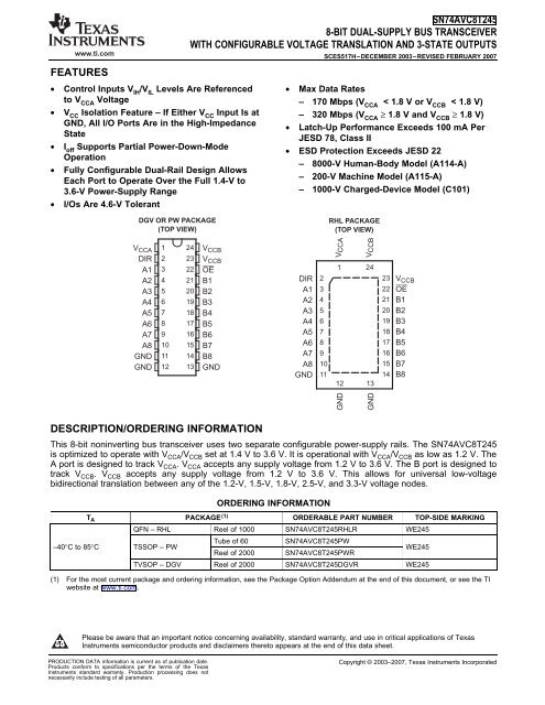
SN74AVC8T245<br />
8-BIT DUAL-SUPPLY BUS TRANSCEIVER<br />
WITH CONFIGURABLE VOLTAGE TRANSLATION AND 3-STATE OUTPUTS<br />
DIR<br />
A1<br />
A2<br />
A3<br />
A4<br />
A5<br />
A6<br />
A7<br />
A8<br />
GND<br />
2<br />
3<br />
4<br />
5<br />
6<br />
7<br />
8<br />
9<br />
10<br />
11<br />
SCES517H–DECEMBER 2003–REVISED FEBRUARY 2007<br />
• Control Inputs VIH /VIL Levels Are Referenced • Max Data Rates<br />
to VCCA Voltage – 170 Mbps (VCCA < 1.8 V or VCCB < 1.8 V)<br />
• VCC Isolation Feature – If Either VCC Input Is at – 320 Mbps (VCCA ≥ 1.8 V and VCCB ≥ 1.8 V)<br />
GND, All I/O Ports Are in the High-Impedance<br />
• Latch-Up Performance Exceeds 100 mA Per<br />
State<br />
JESD 78, Class II<br />
• Ioff Supports Partial Power-Down-Mode<br />
• ESD Protection Exceeds JESD 22<br />
Operation<br />
– 8000-V Human-Body Model (A114-A)<br />
• Fully Configurable Dual-Rail Design Allows<br />
– 200-V Machine Model (A115-A)<br />
Each Port to Operate Over the Full 1.4-V to<br />
3.6-V Power-Supply Range<br />
• I/Os Are 4.6-V Tolerant<br />
– 1000-V Charged-Device Model (C101)<br />
RHL PACKAGE<br />
(TOP VIEW)<br />
VCCA<br />
VCCB<br />
1 24<br />
12 13<br />
This 8-bit noninverting bus transceiver uses two separate configurable power-supply rails. The SN74AVC8T245<br />
is optimized to operate with V CCA/V CCB set at 1.4 V to 3.6 V. It is operational with V CCA/V CCB as low as 1.2 V. The<br />
A port is designed to track V CCA. V CCA accepts any supply voltage from 1.2 V to 3.6 V. The B port is designed to<br />
track V CCB. V CCB accepts any supply voltage from 1.2 V to 3.6 V. This allows for universal low-voltage<br />
bidirectional translation between any of the 1.2-V, 1.5-V, 1.8-V, 2.5-V, and 3.3-V voltage nodes.<br />
ORDERING INFORMATION<br />
GND<br />
GND<br />
23<br />
22<br />
21<br />
20<br />
19<br />
18<br />
17<br />
16<br />
15<br />
14<br />
V CCB<br />
OE<br />
B1<br />
B2<br />
B3<br />
B4<br />
B5<br />
B6<br />
B7<br />
B8<br />
T A PACKAGE (1) ORDERABLE PART NUMBER TOP-SIDE MARKING<br />
QFN – RHL Reel of 1000 SN74AVC8T245RHLR WE245<br />
Tube of 60 SN74AVC8T245PW<br />
–40°C to 85°C TSSOP – PW WE245<br />
Reel of 2000 SN74AVC8T245PWR<br />
TVSOP – DGV Reel of 2000 SN74AVC8T245DGVR WE245<br />
(1) For the most current package and ordering information, see the Package Option Addendum at the end of this document, or see the TI<br />
website at www.ti.com.<br />
Please be aware that an important notice concerning availability, standard warranty, and use in critical applications of Texas<br />
Instruments semiconductor products and disclaimers thereto appears at the end of this data sheet.<br />
PRODUCTION DATA information is current as of publication date. Copyright © 2003–2007, Texas Instruments Incorporated<br />
Products conform to specifications per the terms of the Texas<br />
Instruments standard warranty. Production processing does not<br />
necessarily include testing of all parameters.
SN74AVC8T245<br />
8-BIT DUAL-SUPPLY BUS TRANSCEIVER<br />
WITH CONFIGURABLE VOLTAGE TRANSLATION AND 3-STATE OUTPUTS<br />
SCES517H–DECEMBER 2003–REVISED FEBRUARY 2007<br />
DESCRIPTION/ORDERING INFORMATION (CONTINUED)<br />
DIR<br />
A1<br />
2<br />
3<br />
To Seven Other Channels<br />
22<br />
21<br />
OE<br />
B1<br />
www.ti.com<br />
The SN74AVC8T245 is designed for asynchronous communication between data buses. The device transmits<br />
data from the A bus to the B bus or from the B bus to the A bus, depending on the logic level at the<br />
direction-control (DIR) input. The output-enable (OE) input can be used to disable the outputs so the buses are<br />
effectively isolated.<br />
The SN74AVC8T245 is designed so the control pins (DIR and OE) are supplied by V CCA.<br />
The SN74AVC8T245 solution is compatible with a single-supply system and can be replaced later with a '245<br />
function, with minimal printed circuit board redesign.<br />
This device is fully specified for partial-power-down applications using I off. The I off circuitry disables the outputs,<br />
preventing damaging current backflow through the device when it is powered down.<br />
The V CC isolation feature ensures that if either V CC input is at GND, both ports are in the high-impedance state.<br />
To ensure the high-impedance state during power up or power down, OE shall be tied to V CC through a pullup<br />
resistor; the minimum value of the resistor is determined by the current-sinking capability of the driver.<br />
FUNCTION TABLE<br />
(each 8-bit section)<br />
INPUTS<br />
OE DIR<br />
OPERATION<br />
L L B data to A bus<br />
L H A data to B bus<br />
H X All outputs Hi-Z<br />
LOGIC DIAGRAM (POSITIVE LOGIC)<br />
2 Submit Documentation Feedback
www.ti.com<br />
Absolute Maximum Ratings (1)<br />
over operating free-air temperature range (unless otherwise noted)<br />
V CCA<br />
V CCB<br />
SN74AVC8T245<br />
8-BIT DUAL-SUPPLY BUS TRANSCEIVER<br />
WITH CONFIGURABLE VOLTAGE TRANSLATION AND 3-STATE OUTPUTS<br />
SCES517H–DECEMBER 2003–REVISED FEBRUARY 2007<br />
MIN MAX UNIT<br />
Supply voltage range –0.5 4.6 V<br />
I/O ports (A port) –0.5 4.6<br />
V I Input voltage range (2) I/O ports (B port) –0.5 4.6 V<br />
V O<br />
Voltage range applied to any output<br />
in the high-impedance or power-off state (2)<br />
Control inputs –0.5 4.6<br />
A port –0.5 4.6<br />
B port –0.5 4.6<br />
A port –0.5 V CCA + 0.5<br />
V O Voltage range applied to any output in the high or low state (2)(3) V<br />
B port –0.5 V CCB + 0.5<br />
I IK Input clamp current V I < 0 –50 mA<br />
I OK Output clamp current V O < 0 –50 mA<br />
I O Continuous output current ±50 mA<br />
Continuous current through V CCA, V CCB, or GND ±100 mA<br />
DGV package 86<br />
θ JA Package thermal impedance (4) PW package 88 °C/W<br />
RHL package 43<br />
T stg Storage temperature range –65 150 °C<br />
(1) Stresses beyond those listed under "absolute maximum ratings" may cause permanent damage to the device. These are stress ratings<br />
only, and functional operation of the device at these or any other conditions beyond those indicated under "recommended operating<br />
conditions" is not implied. Exposure to absolute-maximum-rated conditions for extended periods may affect device reliability.<br />
(2) The input voltage and output negative-voltage ratings may be exceeded if the input and output current ratings are observed.<br />
(3) The output positive-voltage rating may be exceeded up to 4.6 V maximum if the output current rating is observed.<br />
(4) The package thermal impedance is calculated in accordance with JESD 51-7.<br />
Submit Documentation Feedback<br />
V<br />
3
SN74AVC8T245<br />
8-BIT DUAL-SUPPLY BUS TRANSCEIVER<br />
WITH CONFIGURABLE VOLTAGE TRANSLATION AND 3-STATE OUTPUTS<br />
SCES517H–DECEMBER 2003–REVISED FEBRUARY 2007<br />
Recommended Operating Conditions (1)(2)(3)<br />
www.ti.com<br />
V CCI V CCO MIN MAX UNIT<br />
V CCA Supply voltage 1.2 3.6 V<br />
V CCB Supply voltage 1.2 3.6 V<br />
VIH High-level<br />
input voltage<br />
Data inputs<br />
1.2 V to 1.95 V<br />
1.95 V to 2.7 V<br />
VCCI × 0.65<br />
1.6 V<br />
2.7 V to 3.6 V 2<br />
VIL Low-level<br />
input voltage<br />
Data inputs<br />
1.2 V to 1.95 V<br />
1.95 V to 2.7 V<br />
VCCI × 0.35<br />
0.7 V<br />
2.7 V to 3.6 V 0.8<br />
1.2 V to 1.95 V VCCA × 0.65<br />
High-level DIR<br />
VIH 1.95 V to 2.7 V 1.6 V<br />
input voltage (referenced to VCCA) 2.7 V to 3.6 V 2<br />
1.2 V to 1.95 V VCCA × 0.35<br />
Low-level DIR<br />
VIL 1.95 V to 2.7 V 0.7 V<br />
input voltage (referenced to VCCA) 2.7 V to 3.6 V 0.8<br />
V I Input voltage 0 3.6 V<br />
Active state 0 V CCO<br />
V O Output voltage V<br />
3-state 0 3.6<br />
1.2 V –3<br />
1.4 V to 1.6 V –6<br />
I OH High-level output current 1.65 V to 1.95 V –8 mA<br />
2.3 V to 2.7 V –9<br />
3 V to 3.6 V –12<br />
1.2 V 3<br />
1.4 V to 1.6 V 6<br />
I OL Low-level output current 1.65 V to 1.95 V 8 mA<br />
2.3 V to 2.7 V 9<br />
3 V to 3.6 V 12<br />
Δt/Δv Input transition rise or fall rate 5 ns/V<br />
T A Operating free-air temperature –40 85 °C<br />
(1) V CCI is the V CC associated with the input port.<br />
(2) V CCO is the V CC associated with the output port.<br />
(3) All unused data inputs of the device must be held at V CCI or GND to ensure proper device operation. Refer to the TI application report,<br />
Implications of Slow or Floating CMOS Inputs, literature number SCBA004.<br />
4 Submit Documentation Feedback
www.ti.com<br />
SN74AVC8T245<br />
8-BIT DUAL-SUPPLY BUS TRANSCEIVER<br />
WITH CONFIGURABLE VOLTAGE TRANSLATION AND 3-STATE OUTPUTS<br />
Electrical Characteristics (1)(2)<br />
over recommended operating free-air temperature range (unless otherwise noted)<br />
SCES517H–DECEMBER 2003–REVISED FEBRUARY 2007<br />
T A = 25°C –40°C to 85°C<br />
PARAMETER TEST CONDITIONS V CCA V CCB UNIT<br />
MIN TYP MAX MIN MAX<br />
I OH = –100 μA 1.2 V to 3.6 V 1.2 V to 3.6 V V CCO – 0.2<br />
I OH = –3 mA 1.2 V 1.2 V 0.95<br />
I OH = –6 mA 1.4 V 1.4 V 1.05<br />
V OH V I = V IH V<br />
I OH = –8 mA 1.65 V 1.65 V 1.2<br />
I OH = –9 mA 2.3 V 2.3 V 1.75<br />
I OH = –12 mA 3 V 3 V 2.3<br />
I OL = 100 μA 1.2 V to 3.6 V 1.2 V to 3.6 V 0.2<br />
I OL = 3 mA 1.2 V 1.2 V 0.15<br />
I OL = 6 mA 1.4 V 1.4 V 0.35<br />
V OL V I = V IL V<br />
I OL = 8 mA 1.65 V 1.65 V 0.45<br />
I OL = 9 mA 2.3 V 2.3 V 0.55<br />
I OL = 12 mA 3 V 3 V 0.7<br />
Control<br />
I I V I = V CCA or GND 1.2 V to 3.6 V 1.2 V to 3.6 V ±0.025 ±0.25 ±1 μA<br />
inputs<br />
A or B<br />
0 V 0 V to 3.6 V ±0.1 ±1 ±5<br />
Ioff VI or VO = 0 to 3.6 V μA<br />
port 0 V to 3.6 V 0 V ±0.1 ±1 ±5<br />
VO = VCCO or GND,<br />
A or B<br />
I (3)<br />
OZ VI = VCCI or GND, 3.6 V 3.6 V ±0.5 ±2.5 ±5 μA<br />
port<br />
OE = VIH 1.2 V to 3.6 V 1.2 V to 3.6 V 15<br />
I CCA V I = V CCI or GND, I O = 0 0 V 3.6 V –2 μA<br />
3.6 V 0 V 15<br />
1.2 V to 3.6 V 1.2 V to 3.6 V 15<br />
I CCB V I = V CCI or GND, I O = 0 0 V 3.6 V 15 μA<br />
IC<br />
CA +<br />
IC<br />
CB<br />
3.6 V 0 V –2<br />
V I = V CCI or GND, I O = 0 1.2 V to 3.6 V 1.2 V to 3.6 V 25 μA<br />
Control<br />
C i V I = 3.3 V or GND 3.3 V 3.3 V 3.5 4.5 pF<br />
inputs<br />
A or B<br />
C io V O = 3.3 V or GND 3.3 V 3.3 V 6 7 pF<br />
port<br />
(1) V CCO is the V CC associated with the output port.<br />
(2) V CCI is the V CC associated with the input port.<br />
(3) For I/O ports, the parameter I OZ includes the input leakage current.<br />
Submit Documentation Feedback<br />
5
SN74AVC8T245<br />
8-BIT DUAL-SUPPLY BUS TRANSCEIVER<br />
WITH CONFIGURABLE VOLTAGE TRANSLATION AND 3-STATE OUTPUTS<br />
SCES517H–DECEMBER 2003–REVISED FEBRUARY 2007<br />
Switching Characteristics<br />
over recommended operating free-air temperature range, VCCA = 1.2 V (see Figure 10)<br />
Switching Characteristics<br />
over recommended operating free-air temperature range, VCCA = 1.5 V ± 0.1 V (see Figure 10)<br />
www.ti.com<br />
FROM TO VCCB = 1.2 V VCCB = 1.5 V VCCB = 1.8 V VCCB = 2.5 V VCCB = 3.3 V<br />
PARAMETER UNIT<br />
(INPUT) (OUTPUT) TYP TYP TYP TYP TYP<br />
t PLH 3.1 2.6 2.5 3 3.5<br />
A B ns<br />
t PHL 3.1 2.6 2.5 3 3.5<br />
t PLH 3.1 2.7 2.5 2.4 2.3<br />
B A ns<br />
t PHL 3.1 2.7 2.5 2.4 2.3<br />
t PZH 5.3 5.3 5.3 5.3 5.3<br />
OE A ns<br />
t PZL 5.3 5.3 5.3 5.3 5.3<br />
t PZH 5.1 4 3.5 3.2 3.1<br />
OE B ns<br />
t PZL 5.1 4 3.5 3.2 3.1<br />
t PHZ 4.8 4.8 4.8 4.8 4.8<br />
OE A ns<br />
t PLZ 4.8 4.8 4.8 4.8 4.8<br />
t PHZ 4.7 4 4.1 4.3 5.1<br />
OE B ns<br />
t PLZ 4.7 4 4.1 4.3 5.1<br />
VCCB = 1.5 V VCCB = 1.8 V VCCB = 2.5 V VCCB = 3.3 V<br />
FROM TO VCCB = 1.2 V<br />
PARAMETER ± 0.1 V ± 0.15 V ± 0.2 V ± 0.3 V UNIT<br />
(INPUT) (OUTPUT)<br />
TYP MIN MAX MIN MAX MIN MAX MIN MAX<br />
t PLH 2.7 0.5 5.4 0.5 4.6 0.5 4.9 0.5 6.8<br />
A B ns<br />
t PHL 2.7 0.5 5.4 0.5 4.6 0.5 4.9 0.5 6.8<br />
t PLH 2.6 0.5 5.4 0.5 5.1 0.5 4.7 0.5 4.5<br />
B A ns<br />
t PHL 2.6 0.5 5.4 0.5 5.1 0.5 4.7 0.5 4.5<br />
t PZH 3.7 1.1 8.7 1.1 8.7 1.1 8.7 1.1 8.7<br />
OE A ns<br />
t PZL 3.7 1.1 8.7 1.1 8.7 1.1 8.7 1.1 8.7<br />
t PZH 4.8 1.1 7.6 1.1 7.1 1 5.6 1 5.2<br />
OE B ns<br />
t PZL 4.8 1.1 7.6 1.1 7.1 1 5.6 1 5.2<br />
t PHZ 3.1 0.5 8.6 0.5 8.6 0.5 8.6 0.5 8.6<br />
OE A ns<br />
t PLZ 3.1 0.5 8.6 0.5 8.6 0.5 8.6 0.5 8.6<br />
t PHZ 4.1 0.5 8.4 0.5 7.6 0.5 7.2 0.5 7.8<br />
OE B ns<br />
t PLZ 4.1 0.5 8.4 0.5 7.6 0.5 7.2 0.5 7.8<br />
6 Submit Documentation Feedback
www.ti.com<br />
SN74AVC8T245<br />
8-BIT DUAL-SUPPLY BUS TRANSCEIVER<br />
WITH CONFIGURABLE VOLTAGE TRANSLATION AND 3-STATE OUTPUTS<br />
Switching Characteristics<br />
over recommended operating free-air temperature range, VCCA = 1.8 V ± 0.15 V (see Figure 10)<br />
Switching Characteristics<br />
over recommended operating free-air temperature range, VCCA = 2.5 V ± 0.2 V (see Figure 10)<br />
SCES517H–DECEMBER 2003–REVISED FEBRUARY 2007<br />
VCCB = 1.5 V VCCB = 1.8 V VCCB = 2.5 V VCCB = 3.3 V<br />
FROM TO VCCB = 1.2 V<br />
PARAMETER ± 0.1 V ± 0.15 V ± 0.2 V ± 0.3 V UNIT<br />
(INPUT) (OUTPUT)<br />
TYP MIN MAX MIN MAX MIN MAX MIN MAX<br />
t PLH 2.5 0.5 5.1 0.5 4.4 0.5 4 0.5 3.9<br />
A B ns<br />
t PHL 2.5 0.5 5.1 0.5 4.4 0.5 4 0.5 3.9<br />
t PLH 2.5 0.5 4.6 0.5 4.4 0.5 3.9 0.5 3.7<br />
B A ns<br />
t PHL 2.5 0.5 4.6 0.5 4.4 0.5 3.9 0.5 3.7<br />
t PZH 3 1 6.8 1 6.8 1 6.8 1 6.8<br />
OE A ns<br />
t PZL 3 1 6.8 1 6.8 1 6.8 1 6.8<br />
t PZH 4.6 1.1 8.2 1 6.7 0.5 5.1 0.5 4.5<br />
OE B ns<br />
t PZL 4.6 1.1 8.2 1 6.7 0.5 5.1 0.5 4.5<br />
t PHZ 2.8 0.5 7.1 0.5 7.1 0.5 7.1 0.5 7.1<br />
OE A ns<br />
t PLZ 2.8 0.5 7.1 0.5 7.1 0.5 7.1 0.5 7.1<br />
t PHZ 3.9 0.5 7.8 0.5 6.9 0.5 6 0.5 5.8<br />
OE B ns<br />
t PLZ 3.9 0.5 7.8 0.5 6.9 0.5 6 0.5 5.8<br />
VCCB = 1.5 V VCCB = 1.8 V VCCB = 2.5 V VCCB = 3.3 V<br />
FROM TO VCCB = 1.2 V<br />
PARAMETER ± 0.1 V ± 0.15 V ± 0.2 V ± 0.3 V UNIT<br />
(INPUT) (OUTPUT)<br />
TYP MIN MAX MIN MAX MIN MAX MIN MAX<br />
t PLH 2.4 0.5 4.7 0.5 3.9 0.5 3.1 0.5 2.8<br />
A B ns<br />
t PHL 2.4 0.5 4.7 0.5 3.9 0.5 3.1 0.5 2.8<br />
t PLH 3 0.5 4.9 0.5 4 0.5 3.1 0.5 2.9<br />
B A ns<br />
t PHL 3 0.5 4.9 0.5 4 0.5 3.1 0.5 2.9<br />
t PZH 2.2 0.5 4.8 0.5 4.8 0.5 4.8 0.5 4.8<br />
OE A ns<br />
t PZL 2.2 0.5 4.8 0.5 4.8 0.5 4.8 0.5 4.8<br />
t PZH 4.5 1.1 7.9 0.5 6.4 0.5 4.6 0.5 4<br />
OE B ns<br />
t PZL 4.5 1.1 7.9 0.5 6.4 0.5 4.6 0.5 4<br />
t PHZ 1.8 0.5 5.1 0.5 5.1 0.5 5.1 0.5 5.1<br />
OE A ns<br />
t PLZ 1.8 0.5 5.1 0.5 5.1 0.5 5.1 0.5 5.1<br />
t PHZ 3.6 0.5 7.1 0.5 6.3 0.5 5.1 0.5 3.9<br />
OE B ns<br />
t PLZ 3.6 0.5 7.1 0.5 6.3 0.5 5.1 0.5 3.9<br />
Submit Documentation Feedback<br />
7
SN74AVC8T245<br />
8-BIT DUAL-SUPPLY BUS TRANSCEIVER<br />
WITH CONFIGURABLE VOLTAGE TRANSLATION AND 3-STATE OUTPUTS<br />
SCES517H–DECEMBER 2003–REVISED FEBRUARY 2007<br />
Switching Characteristics<br />
over recommended operating free-air temperature range, VCCA = 3.3 V ± 0.3 V (see Figure 10)<br />
Operating Characteristics<br />
TA = 25°C<br />
www.ti.com<br />
VCCB = 1.5 V VCCB = 1.8 V VCCB = 2.5 V VCCB = 3.3 V<br />
FROM TO VCCB = 1.2 V<br />
PARAMETER ± 0.1 V ± 0.15 V ± 0.2 V ± 0.3 V UNIT<br />
(INPUT) (OUTPUT)<br />
TYP MIN MAX MIN MAX MIN MAX MIN MAX<br />
t PLH 2.3 0.5 4.5 0.5 3.7 0.5 2.9 0.5 2.5<br />
A B ns<br />
t PHL 2.3 0.5 4.5 0.5 3.3 0.5 2.9 0.5 2.5<br />
t PLH 3.5 0.5 6.8 0.5 3.9 0.5 2.8 0.5 2.5<br />
B A ns<br />
t PHL 3.5 0.5 6.8 0.5 3.9 0.5 2.8 0.5 2.5<br />
t PZH 2 0.5 4 0.5 4 0.5 4 0.5 4<br />
OE A ns<br />
t PZL 2 0.5 4 0.5 4 0.5 4 0.5 4<br />
t PZH 4.5 1.1 7.8 0.5 6.2 0.5 4.5 0.5 3.9<br />
OE B ns<br />
t PZL 4.5 1.1 7.8 0.5 6.2 0.5 4.5 0.5 3.9<br />
t PHZ 1.7 0.5 4 0.5 4 0.5 4 0.5 4<br />
OE A ns<br />
t PLZ 1.7 0.5 4 0.5 4 0.5 4 0.5 4<br />
t PHZ 3.4 0.5 6.9 0.5 6 0.5 4.8 0.5 4.2<br />
OE B ns<br />
t PLZ 3.4 0.5 6.9 0.5 6 0.5 4.8 0.5 4.2<br />
VCCA = VCCA = VCCA = VCCA = VCCA =<br />
TEST<br />
PARAMETER VCCB = 1.2 V VCCB = 1.5 V VCCB = 1.8 V VCCB = 2.5 V VCCB = 3.3 V UNIT<br />
CONDITIONS<br />
TYP TYP TYP TYP TYP<br />
Outputs<br />
1 1 1 1 1<br />
enabled<br />
A to B<br />
Outputs<br />
C 1 1 1 1 1<br />
disabled<br />
L = 0,<br />
C (1)<br />
pdA f = 10 MHz, pF<br />
Outputs tr = tf = 1 ns 12 12 12 13 14<br />
enabled<br />
B to A<br />
Outputs<br />
1 1 1 1 1<br />
disabled<br />
Outputs<br />
12 12 12 13 14<br />
enabled<br />
A to B<br />
Outputs<br />
C 1 1 1 1 1<br />
disabled<br />
L = 0,<br />
C (1)<br />
pdB f = 10 MHz, pF<br />
Outputs tr = tf = 1 ns 1 1 1 1 1<br />
enabled<br />
B to A<br />
Outputs<br />
1 1 1 1 1<br />
disabled<br />
(1) Power dissipation capacitance per transceiver<br />
V CCB<br />
Table 1. Typical Total Static Power Consumption (I CCA + I CCB)<br />
V CCA<br />
0 V 1.2 V 1.5 V 1.8 V 2.5 V 3.3 V<br />
0 V 0
www.ti.com<br />
TYPICAL CHARACTERISTICS<br />
Typical Propagation Delay (A to B) vs Load Capacitance<br />
TA = 25°C, VCCA = 1.2 V<br />
t PD − ns<br />
6<br />
5<br />
4<br />
3<br />
2<br />
1<br />
0<br />
0 10 20 30 40 50<br />
C L − pF<br />
Typical Propagation Delay (A to B) vs Load Capacitance<br />
TA = 25°C, VCCA = 1.5 V<br />
t PLH − ns<br />
6<br />
5<br />
4<br />
3<br />
2<br />
1<br />
0<br />
0 10 20 30 40 50 60<br />
C L − pF<br />
SN74AVC8T245<br />
8-BIT DUAL-SUPPLY BUS TRANSCEIVER<br />
WITH CONFIGURABLE VOLTAGE TRANSLATION AND 3-STATE OUTPUTS<br />
V CCB = 1.2 V<br />
V CCB = 1.5 V<br />
V CCB = 1.8 V<br />
V CCB = 2.5 V<br />
V CCB = 3.3 V<br />
Figure 1.<br />
t PHL − ns<br />
6<br />
5<br />
4<br />
3<br />
2<br />
1<br />
SCES517H–DECEMBER 2003–REVISED FEBRUARY 2007<br />
V CCB = 1.2 V<br />
V CCB = 1.5 V<br />
V CCB = 1.8 V<br />
V CCB = 2.5 V<br />
V CCB = 3.3 V<br />
60<br />
0<br />
0 10 20 30 40 50 60<br />
C L − pF<br />
Figure 2. Figure 3.<br />
Submit Documentation Feedback<br />
V CCB = 1.2 V<br />
V CCB = 1.5 V<br />
V CCB = 1.8 V<br />
V CCB = 2.5 V<br />
V CCB = 3.3 V<br />
9
SN74AVC8T245<br />
8-BIT DUAL-SUPPLY BUS TRANSCEIVER<br />
WITH CONFIGURABLE VOLTAGE TRANSLATION AND 3-STATE OUTPUTS<br />
SCES517H–DECEMBER 2003–REVISED FEBRUARY 2007<br />
Typical Propagation Delay (A to B) vs Load Capacitance<br />
TA = 25°C, VCCA = 1.8 V<br />
t PLH − ns<br />
6<br />
5<br />
4<br />
3<br />
2<br />
1<br />
V CCB = 1.2 V<br />
V CCB = 1.5 V<br />
V CCB = 1.8 V<br />
V CCB = 2.5 V<br />
V CCB = 3.3 V<br />
0<br />
0 10 20 30 40 50 60<br />
C L − pF<br />
Typical Propagation Delay (A to B) vs Load Capacitance<br />
TA = 25°C, VCCA = 2.5 V<br />
t PLH − ns<br />
6<br />
5<br />
4<br />
3<br />
2<br />
1<br />
0<br />
V CCB = 1.2 V<br />
V CCB = 1.5 V<br />
V CCB = 1.8 V<br />
V CCB = 2.5 V<br />
V CCB = 3.3 V<br />
0 10 20 30 40 50 60<br />
C L − pF<br />
TYPICAL CHARACTERISTICS (continued)<br />
t PHL − ns<br />
t PHL − ns<br />
6<br />
5<br />
4<br />
3<br />
2<br />
1<br />
V CCB = 1.2 V<br />
V CCB = 1.5 V<br />
V CCB = 1.8 V<br />
V CCB = 2.5 V<br />
V CCB = 3.3 V<br />
www.ti.com<br />
0<br />
0 10 20 30 40 50 60<br />
6<br />
5<br />
4<br />
3<br />
2<br />
1<br />
V CCB = 1.2 V<br />
V CCB = 1.5 V<br />
V CCB = 1.8 V<br />
V CCB = 2.5 V<br />
V CCB = 3.3 V<br />
C L − pF<br />
Figure 4. Figure 5.<br />
0<br />
0 10 20 30 40 50 60<br />
C L − pF<br />
Figure 6. Figure 7.<br />
10 Submit Documentation Feedback
www.ti.com<br />
Typical Propagation Delay (A to B) vs Load Capacitance<br />
TA = 25°C, VCCA = 3.3 V<br />
t PLH − ns<br />
6<br />
5<br />
4<br />
3<br />
2<br />
1<br />
0<br />
V CCB = 1.2 V<br />
V CCB = 1.5 V<br />
V CCB = 1.8 V<br />
V CCB = 2.5 V<br />
V CCB = 3.3 V<br />
0 10 20 30 40 50 60<br />
C L − pF<br />
SN74AVC8T245<br />
8-BIT DUAL-SUPPLY BUS TRANSCEIVER<br />
WITH CONFIGURABLE VOLTAGE TRANSLATION AND 3-STATE OUTPUTS<br />
TYPICAL CHARACTERISTICS (continued)<br />
t PHL − ns<br />
6<br />
5<br />
4<br />
3<br />
2<br />
1<br />
SCES517H–DECEMBER 2003–REVISED FEBRUARY 2007<br />
V CCB = 1.2 V<br />
V CCB = 1.5 V<br />
V CCB = 1.8 V<br />
V CCB = 2.5 V<br />
V CCB = 3.3 V<br />
0<br />
0 10 20 30 40 50 60<br />
C L − pF<br />
Figure 8. Figure 9.<br />
Submit Documentation Feedback<br />
11
SN74AVC8T245<br />
8-BIT DUAL-SUPPLY BUS TRANSCEIVER<br />
WITH CONFIGURABLE VOLTAGE TRANSLATION AND 3-STATE OUTPUTS<br />
SCES517H–DECEMBER 2003–REVISED FEBRUARY 2007<br />
From Output<br />
Under Test<br />
C L<br />
(see Note A)<br />
Input<br />
Output<br />
VCCO 1.2 V<br />
1.5 V ± 0.1 V<br />
1.8 V ± 0.15 V<br />
2.5 V ± 0.2 V<br />
3.3 V ± 0.3 V<br />
t PLH<br />
PARAMETER MEASUREMENT INFORMATION<br />
R L<br />
R L<br />
LOAD CIRCUIT<br />
C L<br />
15 pF<br />
15 pF<br />
15 pF<br />
15 pF<br />
15 pF<br />
R L<br />
2 kΩ<br />
2 kΩ<br />
2 kΩ<br />
2 kΩ<br />
2 kΩ<br />
S1<br />
V CCI/2 V CCI/2<br />
t PHL<br />
2 × V CCO<br />
Open<br />
GND<br />
V CCI<br />
0 V<br />
VOH VCCO/2 VCCO/2 VOL VOLTAGE WAVEFORMS<br />
PROPAGATION DELAY TIMES<br />
V TP<br />
0.1 V<br />
0.1 V<br />
0.15 V<br />
0.15 V<br />
0.3 V<br />
Input<br />
Output<br />
Control<br />
(low-level<br />
enabling)<br />
Output<br />
Waveform 1<br />
S1 at 2 × V CCO<br />
(see Note B)<br />
Output<br />
Waveform 2<br />
S1 at GND<br />
(see Note B)<br />
t PZL<br />
t PZH<br />
TEST S1<br />
t pd<br />
t PLZ/t PZL<br />
t PHZ/t PZH<br />
t w<br />
V CCI/2 V CCI/2<br />
VOLTAGE WAVEFORMS<br />
PULSE DURATION<br />
V CCA/2<br />
Open<br />
2 × VCCO GND<br />
V CCO/2<br />
V CCO/2<br />
V CCA/2<br />
VOLTAGE WAVEFORMS<br />
ENABLE AND DISABLE TIMES<br />
www.ti.com<br />
t PLZ<br />
V OL + V TP<br />
t PHZ<br />
V OH − V TP<br />
NOTES: A. C L includes probe and jig capacitance.<br />
B. Waveform 1 is for an output with internal conditions such that the output is low, except when disabled by the output control.<br />
Waveform 2 is for an output with internal conditions such that the output is high, except when disabled by the output control.<br />
C. All input pulses are supplied by generators having the following characteristics: PRR10 MHz, Z O = 50 Ω, dv/dt ≥1 V/ns.<br />
D. The outputs are measured one at a time, with one transition per measurement.<br />
E. t PLZ and t PHZ are the same as t dis.<br />
F. t PZL and t PZH are the same as t en.<br />
G. t PLH and t PHL are the same as t pd.<br />
H. V CCI is the V CC associated with the input port.<br />
I. V CCO is the V CC associated with the output port.<br />
Figure 10. Load Circuit and Voltage Waveforms<br />
12 Submit Documentation Feedback<br />
V CCI<br />
0 V<br />
V CCA<br />
0 V<br />
V CCO<br />
V OL<br />
V OH<br />
0 V
PACKAGING INFORMATION<br />
Orderable Device Status (1)<br />
Package<br />
Type<br />
Package<br />
Drawing<br />
Pins Package<br />
Qty<br />
74AVC8T245DGVRE4 ACTIVE TVSOP DGV 24 2000 Green (RoHS &<br />
no Sb/Br)<br />
74AVC8T245DGVRG4 ACTIVE TVSOP DGV 24 2000 Green (RoHS &<br />
no Sb/Br)<br />
74AVC8T245RHLRG4 ACTIVE QFN RHL 24 1000 Green (RoHS &<br />
no Sb/Br)<br />
SN74AVC8T245DGVR ACTIVE TVSOP DGV 24 2000 Green (RoHS &<br />
no Sb/Br)<br />
SN74AVC8T245PW ACTIVE TSSOP PW 24 60 Green (RoHS &<br />
no Sb/Br)<br />
SN74AVC8T245PWE4 ACTIVE TSSOP PW 24 60 Green (RoHS &<br />
no Sb/Br)<br />
SN74AVC8T245PWG4 ACTIVE TSSOP PW 24 60 Green (RoHS &<br />
no Sb/Br)<br />
SN74AVC8T245PWR ACTIVE TSSOP PW 24 2000 Green (RoHS &<br />
no Sb/Br)<br />
SN74AVC8T245PWRE4 ACTIVE TSSOP PW 24 2000 Green (RoHS &<br />
no Sb/Br)<br />
SN74AVC8T245PWRG4 ACTIVE TSSOP PW 24 2000 Green (RoHS &<br />
no Sb/Br)<br />
SN74AVC8T245RHLR ACTIVE QFN RHL 24 1000 Green (RoHS &<br />
no Sb/Br)<br />
Eco Plan (2) Lead/Ball Finish MSL Peak Temp (3)<br />
CU NIPDAU Level-1-260C-UNLIM<br />
CU NIPDAU Level-1-260C-UNLIM<br />
CU NIPDAU Level-2-260C-1 YEAR<br />
CU NIPDAU Level-1-260C-UNLIM<br />
CU NIPDAU Level-1-260C-UNLIM<br />
CU NIPDAU Level-1-260C-UNLIM<br />
CU NIPDAU Level-1-260C-UNLIM<br />
CU NIPDAU Level-1-260C-UNLIM<br />
CU NIPDAU Level-1-260C-UNLIM<br />
CU NIPDAU Level-1-260C-UNLIM<br />
CU NIPDAU Level-2-260C-1 YEAR<br />
(1) The marketing status values are defined as follows:<br />
ACTIVE: Product device recommended for new designs.<br />
LIFEBUY: TI has announced that the device will be discontinued, and a lifetime-buy period is in effect.<br />
NRND: Not recommended for new designs. Device is in production to support existing customers, but TI does not recommend using this part in<br />
a new design.<br />
PREVIEW: Device has been announced but is not in production. Samples may or may not be available.<br />
OBSOLETE: TI has discontinued the production of the device.<br />
(2) Eco Plan - The planned eco-friendly classification: Pb-Free (RoHS), Pb-Free (RoHS Exempt), or Green (RoHS & no Sb/Br) - please check<br />
http://www.ti.com/productcontent for the latest availability information and additional product content details.<br />
TBD: The Pb-Free/Green conversion plan has not been defined.<br />
Pb-Free (RoHS): TI's terms "Lead-Free" or "Pb-Free" mean semiconductor products that are compatible with the current RoHS requirements<br />
for all 6 substances, including the requirement that lead not exceed 0.1% by weight in homogeneous materials. Where designed to be soldered<br />
at high temperatures, TI Pb-Free products are suitable for use in specified lead-free processes.<br />
Pb-Free (RoHS Exempt): This component has a RoHS exemption for either 1) lead-based flip-chip solder bumps used between the die and<br />
package, or 2) lead-based die adhesive used between the die and leadframe. The component is otherwise considered Pb-Free (RoHS<br />
compatible) as defined above.<br />
Green (RoHS & no Sb/Br): TI defines "Green" to mean Pb-Free (RoHS compatible), and free of Bromine (Br) and Antimony (Sb) based flame<br />
retardants (Br or Sb do not exceed 0.1% by weight in homogeneous material)<br />
(3) MSL, Peak Temp. -- The Moisture Sensitivity Level rating according to the JEDEC industry standard classifications, and peak solder<br />
temperature.<br />
PACKAGE OPTION ADDENDUM<br />
www.ti.com 26-Mar-2010<br />
Important Information and Disclaimer:The information provided on this page represents TI's knowledge and belief as of the date that it is<br />
provided. TI bases its knowledge and belief on information provided by third parties, and makes no representation or warranty as to the<br />
accuracy of such information. Efforts are underway to better integrate information from third parties. TI has taken and continues to take<br />
reasonable steps to provide representative and accurate information but may not have conducted destructive testing or chemical analysis on<br />
incoming materials and chemicals. TI and TI suppliers consider certain information to be proprietary, and thus CAS numbers and other limited<br />
information may not be available for release.<br />
In no event shall TI's liability arising out of such information exceed the total purchase price of the TI part(s) at issue in this document sold by TI<br />
Addendum-Page 1
to Customer on an annual basis.<br />
OTHER QUALIFIED VERSIONS OF SN74AVC8T245 :<br />
• Automotive: SN74AVC8T245-Q1<br />
NOTE: Qualified Version Definitions:<br />
• Automotive - Q100 devices qualified for high-reliability automotive applications targeting zero defects<br />
PACKAGE OPTION ADDENDUM<br />
www.ti.com 26-Mar-2010<br />
Addendum-Page 2
TAPE AND REEL INFORMATION<br />
*All dimensions are nominal<br />
Device Package<br />
Type<br />
Package<br />
Drawing<br />
Pins SPQ Reel<br />
Diameter<br />
(mm)<br />
PACKAGE MATERIALS INFORMATION<br />
www.ti.com 25-Mar-2010<br />
Reel<br />
Width<br />
W1 (mm)<br />
A0<br />
(mm)<br />
B0<br />
(mm)<br />
K0<br />
(mm)<br />
P1<br />
(mm)<br />
W<br />
(mm)<br />
Pin1<br />
Quadrant<br />
SN74AVC8T245DGVR TVSOP DGV 24 2000 330.0 12.4 7.0 5.6 1.6 8.0 12.0 Q1<br />
SN74AVC8T245PWR TSSOP PW 24 2000 330.0 16.4 6.95 8.3 1.6 8.0 16.0 Q1<br />
SN74AVC8T245RHLR QFN RHL 24 1000 180.0 12.4 3.8 5.8 1.2 8.0 12.0 Q1<br />
Pack Materials-Page 1
*All dimensions are nominal<br />
PACKAGE MATERIALS INFORMATION<br />
www.ti.com 25-Mar-2010<br />
Device Package Type Package Drawing Pins SPQ Length (mm) Width (mm) Height (mm)<br />
SN74AVC8T245DGVR TVSOP DGV 24 2000 346.0 346.0 29.0<br />
SN74AVC8T245PWR TSSOP PW 24 2000 346.0 346.0 33.0<br />
SN74AVC8T245RHLR QFN RHL 24 1000 190.5 212.7 31.8<br />
Pack Materials-Page 2
POST OFFICE BOX 655303 • DALLAS, TEXAS 75265<br />
MECHANICAL DATA<br />
MPDS006C – FEBRUARY 1996 – REVISED AUGUST 2000<br />
DGV (R-PDSO-G**) PLASTIC SMALL-OUTLINE<br />
24 PINS SHOWN<br />
0,40<br />
1,20 MAX<br />
DIM<br />
PINS **<br />
0,23<br />
0,13<br />
24 13<br />
1 12<br />
A<br />
A MAX<br />
A MIN<br />
14<br />
3,70<br />
0,15<br />
0,05<br />
16<br />
3,70<br />
0,07<br />
4,50<br />
4,30<br />
M<br />
6,60<br />
6,20<br />
Seating Plane<br />
20<br />
5,10<br />
3,50 3,50 4,90<br />
0,08<br />
24<br />
5,10<br />
4,90<br />
38<br />
7,90<br />
7,70<br />
0,16 NOM<br />
0°–8°<br />
NOTES: A. All linear dimensions are in millimeters.<br />
B. This drawing is subject to change without notice.<br />
C. Body dimensions do not include mold flash or protrusion, not to exceed 0,15 per side.<br />
D. Falls within JEDEC: 24/48 Pins – MO-153<br />
14/16/20/56 Pins – MO-194<br />
48<br />
9,80<br />
9,60<br />
Gage Plane<br />
56<br />
11,40<br />
11,20<br />
0,25<br />
0,75<br />
0,50<br />
4073251/E 08/00
POST OFFICE BOX 655303 • DALLAS, TEXAS 75265<br />
MECHANICAL DATA<br />
MTSS001C – JANUARY 1995 – REVISED FEBRUARY 1999<br />
PW (R-PDSO-G**) PLASTIC SMALL-OUTLINE PACKAGE<br />
14 PINS SHOWN<br />
0,65<br />
14<br />
1<br />
1,20 MAX<br />
A<br />
DIM<br />
A MAX<br />
A MIN<br />
7<br />
PINS **<br />
8<br />
0,15<br />
0,05<br />
0,30<br />
0,19<br />
8<br />
3,10<br />
2,90<br />
4,50<br />
4,30<br />
0,10<br />
6,60<br />
6,20<br />
M<br />
Seating Plane<br />
14<br />
5,10<br />
4,90<br />
0,10<br />
16<br />
5,10<br />
4,90<br />
20<br />
6,60<br />
6,40<br />
0,15 NOM<br />
0°–8°<br />
NOTES: A. All linear dimensions are in millimeters.<br />
B. This drawing is subject to change without notice.<br />
C. Body dimensions do not include mold flash or protrusion not to exceed 0,15.<br />
D. Falls within JEDEC MO-153<br />
24<br />
7,90<br />
7,70<br />
Gage Plane<br />
28<br />
9,80<br />
9,60<br />
0,25<br />
0,75<br />
0,50<br />
4040064/F 01/97
IMPORTANT NOTICE<br />
Texas Instruments Incorporated and its subsidiaries (TI) reserve the right to make corrections, modifications, enhancements, improvements,<br />
and other changes to its products and services at any time and to discontinue any product or service without notice. Customers should<br />
obtain the latest relevant information before placing orders and should verify that such information is current and complete. All products are<br />
sold subject to TI’s terms and conditions of sale supplied at the time of order acknowledgment.<br />
TI warrants performance of its hardware products to the specifications applicable at the time of sale in accordance with TI’s standard<br />
warranty. Testing and other quality control techniques are used to the extent TI deems necessary to support this warranty. Except where<br />
mandated by government requirements, testing of all parameters of each product is not necessarily performed.<br />
TI assumes no liability for applications assistance or customer product design. Customers are responsible for their products and<br />
applications using TI components. To minimize the risks associated with customer products and applications, customers should provide<br />
adequate design and operating safeguards.<br />
TI does not warrant or represent that any license, either express or implied, is granted under any TI patent right, copyright, mask work right,<br />
or other TI intellectual property right relating to any combination, machine, or process in which TI products or services are used. Information<br />
published by TI regarding third-party products or services does not constitute a license from TI to use such products or services or a<br />
warranty or endorsement thereof. Use of such information may require a license from a third party under the patents or other intellectual<br />
property of the third party, or a license from TI under the patents or other intellectual property of TI.<br />
Reproduction of TI information in TI data books or data sheets is permissible only if reproduction is without alteration and is accompanied<br />
by all associated warranties, conditions, limitations, and notices. Reproduction of this information with alteration is an unfair and deceptive<br />
business practice. TI is not responsible or liable for such altered documentation. Information of third parties may be subject to additional<br />
restrictions.<br />
Resale of TI products or services with statements different from or beyond the parameters stated by TI for that product or service voids all<br />
express and any implied warranties for the associated TI product or service and is an unfair and deceptive business practice. TI is not<br />
responsible or liable for any such statements.<br />
TI products are not authorized for use in safety-critical applications (such as life support) where a failure of the TI product would reasonably<br />
be expected to cause severe personal injury or death, unless officers of the parties have executed an agreement specifically governing<br />
such use. Buyers represent that they have all necessary expertise in the safety and regulatory ramifications of their applications, and<br />
acknowledge and agree that they are solely responsible for all legal, regulatory and safety-related requirements concerning their products<br />
and any use of TI products in such safety-critical applications, notwithstanding any applications-related information or support that may be<br />
provided by TI. Further, Buyers must fully indemnify TI and its representatives against any damages arising out of the use of TI products in<br />
such safety-critical applications.<br />
TI products are neither designed nor intended for use in military/aerospace applications or environments unless the TI products are<br />
specifically designated by TI as military-grade or "enhanced plastic." Only products designated by TI as military-grade meet military<br />
specifications. Buyers acknowledge and agree that any such use of TI products which TI has not designated as military-grade is solely at<br />
the Buyer's risk, and that they are solely responsible for compliance with all legal and regulatory requirements in connection with such use.<br />
TI products are neither designed nor intended for use in automotive applications or environments unless the specific TI products are<br />
designated by TI as compliant with ISO/TS 16949 requirements. Buyers acknowledge and agree that, if they use any non-designated<br />
products in automotive applications, TI will not be responsible for any failure to meet such requirements.<br />
Following are URLs where you can obtain information on other Texas Instruments products and application solutions:<br />
Products Applications<br />
Amplifiers amplifier.ti.com Audio www.ti.com/audio<br />
Data Converters dataconverter.ti.com Automotive www.ti.com/automotive<br />
DLP® Products www.dlp.com Communications and www.ti.com/communications<br />
Telecom<br />
DSP dsp.ti.com Computers and www.ti.com/computers<br />
Peripherals<br />
Clocks and Timers www.ti.com/clocks Consumer Electronics www.ti.com/consumer-apps<br />
Interface interface.ti.com Energy www.ti.com/energy<br />
Logic logic.ti.com Industrial www.ti.com/industrial<br />
Power Mgmt power.ti.com Medical www.ti.com/medical<br />
Microcontrollers microcontroller.ti.com Security www.ti.com/security<br />
RFID www.ti-rfid.com Space, Avionics & www.ti.com/space-avionics-defense<br />
Defense<br />
RF/IF and ZigBee® Solutions www.ti.com/lprf Video and Imaging www.ti.com/video<br />
Wireless www.ti.com/wireless-apps<br />
Mailing Address: Texas Instruments, Post Office Box 655303, Dallas, Texas 75265<br />
Copyright © 2010, Texas Instruments Incorporated