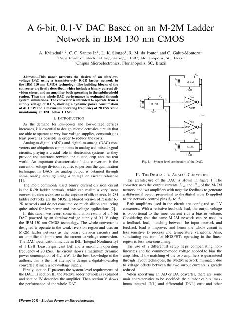
A 6-bit, 0.1-V DAC Based on an M-2M Ladder Network in IBM 130 nm CMOS
A 6-bit, 0.1-V DAC Based on an M-2M Ladder Network in IBM 130 nm CMOS
A 6-bit, 0.1-V DAC Based on an M-2M Ladder Network in IBM 130 nm CMOS

Create successful ePaper yourself
Turn your PDF publications into a flip-book with our unique Google optimized e-Paper software.
A 6-<str<strong>on</strong>g>bit</str<strong>on</strong>g>, <str<strong>on</strong>g>0.1</str<strong>on</strong>g>-V <str<strong>on</strong>g>DAC</str<strong>on</strong>g> <str<strong>on</strong>g>Based</str<strong>on</strong>g> <strong>on</strong> <strong>an</strong> M-<strong>2M</strong> <strong>Ladder</strong><br />
<strong>Network</strong> <strong>in</strong> <strong>IBM</strong> <strong>130</strong> <strong>nm</strong> <strong>CMOS</strong><br />
A. Kvitschal 1 2 , C. C. S<strong>an</strong>tos Jr. 1 , L. K. Sl<strong>on</strong>go 1 , R. M. da P<strong>on</strong>te 1 <strong>an</strong>d C. Galup-M<strong>on</strong>toro 1<br />
1 Department of Electrical Eng<strong>in</strong>eer<strong>in</strong>g, UFSC, Flori<strong>an</strong>ópolis, SC, Brazil<br />
2 Chipus Microelectr<strong>on</strong>ics, Flori<strong>an</strong>ópolis, SC, Brazil<br />
Abstract—This paper presents the design of <strong>an</strong> ultralowvoltage<br />
<str<strong>on</strong>g>DAC</str<strong>on</strong>g> us<strong>in</strong>g a tr<strong>an</strong>sistor-<strong>on</strong>ly R-2R ladder network <strong>in</strong><br />
the <strong>IBM</strong> <strong>130</strong> <strong>nm</strong> <strong>CMOS</strong> technology. The build<strong>in</strong>g blocks of the<br />
c<strong>on</strong>verter are firstly described, which <strong>in</strong>clude a b<strong>in</strong>ary current divisi<strong>on</strong><br />
circuit <strong>an</strong>d <strong>an</strong> amplifier both operat<strong>in</strong>g <strong>in</strong> the subthreshold<br />
regi<strong>on</strong>. Then the whole <str<strong>on</strong>g>DAC</str<strong>on</strong>g> perform<strong>an</strong>ce is evaluated through<br />
system simulati<strong>on</strong>s. The c<strong>on</strong>verter is <strong>in</strong>tended to operate from a<br />
supply voltage of <str<strong>on</strong>g>0.1</str<strong>on</strong>g> V, show<strong>in</strong>g a dynamic power c<strong>on</strong>sumpti<strong>on</strong><br />
of 41.1 nW <strong>an</strong>d a maximum operat<strong>in</strong>g frequency of 20 kS/s while<br />
ma<strong>in</strong>ta<strong>in</strong><strong>in</strong>g <strong>an</strong> INL below 1 LSB.<br />
I. INTRODUCTION<br />
As the dem<strong>an</strong>d for low-power <strong>an</strong>d low-voltage devices<br />
<strong>in</strong>creases, it is essential to design microelectr<strong>on</strong>ics circuits that<br />
are able to operate at very low-voltage supplies, c<strong>on</strong>sum<strong>in</strong>g as<br />
least power as possible <strong>in</strong> order to reduce the costs.<br />
Analog-to-digital (ADC) <strong>an</strong>d digital-to-<strong>an</strong>alog (<str<strong>on</strong>g>DAC</str<strong>on</strong>g>) c<strong>on</strong>verters<br />
are ubiquitous comp<strong>on</strong>ents <strong>in</strong> <strong>an</strong>alog <strong>an</strong>d mixed-signal<br />
circuits, play<strong>in</strong>g a crucial role <strong>in</strong> electr<strong>on</strong>ics systems, as they<br />
provide the <strong>in</strong>terface between the silic<strong>on</strong> chip <strong>an</strong>d the real<br />
world. An import<strong>an</strong>t characteristic of data c<strong>on</strong>verters is the<br />
current or voltage divisi<strong>on</strong> required to perform the qu<strong>an</strong>tizati<strong>on</strong><br />
technique. In <str<strong>on</strong>g>DAC</str<strong>on</strong>g>s the <strong>an</strong>alog output is obta<strong>in</strong>ed through<br />
some scal<strong>in</strong>g circuitry us<strong>in</strong>g a voltage or current reference<br />
[1].<br />
The most comm<strong>on</strong>ly used b<strong>in</strong>ary current divisi<strong>on</strong> circuit<br />
is the R-2R ladder network, which c<strong>an</strong> realize a very l<strong>in</strong>ear<br />
current divisi<strong>on</strong> technique at the expense of silic<strong>on</strong> area. M-<strong>2M</strong><br />
ladder networks are the MOSFET-based versi<strong>on</strong> of resistor R-<br />
2R networks <strong>an</strong>d do not c<strong>on</strong>sume too much silic<strong>on</strong> area, be<strong>in</strong>g<br />
quite suited for low-power <strong>an</strong>d low-voltage applicati<strong>on</strong>s [2].<br />
In this paper, we report some simulati<strong>on</strong> results of a 6-<str<strong>on</strong>g>bit</str<strong>on</strong>g><br />
<str<strong>on</strong>g>DAC</str<strong>on</strong>g> powered by <strong>an</strong> ultralow-voltage supply of <str<strong>on</strong>g>0.1</str<strong>on</strong>g> V us<strong>in</strong>g<br />
the <strong>IBM</strong> <strong>130</strong> <strong>nm</strong> <strong>CMOS</strong> technology. The whole c<strong>on</strong>verter is<br />
designed to operate <strong>in</strong> the weak-<strong>in</strong>versi<strong>on</strong> regi<strong>on</strong> <strong>an</strong>d uses <strong>an</strong><br />
M-<strong>2M</strong> ladder network as the b<strong>in</strong>ary divisi<strong>on</strong> circuitry <strong>an</strong>d<br />
<strong>an</strong> amplifier to implement the current-to-voltage c<strong>on</strong>versi<strong>on</strong>.<br />
The <str<strong>on</strong>g>DAC</str<strong>on</strong>g> specificati<strong>on</strong>s <strong>in</strong>clude <strong>an</strong> INL (Integral N<strong>on</strong>l<strong>in</strong>earity)<br />
of 1 LSB (Least Signific<strong>an</strong>t Bit) <strong>an</strong>d a maximum operat<strong>in</strong>g<br />
frequency of 20 kS/s. The circuit shows a maximum dynamic<br />
power c<strong>on</strong>sumpti<strong>on</strong> of 41.1 nW. To the best knowledge of the<br />
authors, this is the first attempt to design a digital-to-<strong>an</strong>alog<br />
c<strong>on</strong>verter at such a low-voltage supply.<br />
Firstly, secti<strong>on</strong> II presents the system-level requirements of<br />
the <str<strong>on</strong>g>DAC</str<strong>on</strong>g>. In secti<strong>on</strong> III, the M-<strong>2M</strong> ladder network is expla<strong>in</strong>ed<br />
<strong>an</strong>d secti<strong>on</strong> IV describes the amplifier. Then secti<strong>on</strong> V shows<br />
the perform<strong>an</strong>ce of the whole <str<strong>on</strong>g>DAC</str<strong>on</strong>g>.<br />
d 5<br />
...<br />
d0<br />
V ref<br />
M−<strong>2M</strong><br />
GND<br />
V B<br />
I out<br />
I out<br />
d 5<br />
d0<br />
d 5<br />
d0<br />
M−<strong>2M</strong><br />
GND<br />
AMP<br />
AMP<br />
V DD<br />
GND<br />
V DD<br />
M−<strong>2M</strong><br />
GND<br />
GND<br />
Fig. 1. System-level architecture of the <str<strong>on</strong>g>DAC</str<strong>on</strong>g>.<br />
V B<br />
V B<br />
V diff<br />
II. THE DIGITAL-TO-ANALOG CONVERTER<br />
The architecture of the <str<strong>on</strong>g>DAC</str<strong>on</strong>g> is shown <strong>in</strong> figure 1. The<br />
c<strong>on</strong>verter uses the output currents Iout <strong>an</strong>d I ′ outof the M-<strong>2M</strong><br />
network <strong>an</strong>d two amplifiers with negative feedback to generate<br />
a differential output proport<strong>in</strong>al to the digital word D applied<br />
to the network c<strong>on</strong>trol p<strong>in</strong>s d0 to d5.<br />
Both amplifiers used <strong>in</strong> the circuit are c<strong>on</strong>figured as I-V<br />
c<strong>on</strong>verters. With a resistive feedback load, the output voltage<br />
is proporti<strong>on</strong>al to the <strong>in</strong>put current plus a bias<strong>in</strong>g voltage.<br />
C<strong>on</strong>sider<strong>in</strong>g that the same M-<strong>2M</strong> network c<strong>an</strong> be used as<br />
a feedback load, match<strong>in</strong>g between the <strong>in</strong>put network <strong>an</strong>d<br />
feedback load is improved <strong>an</strong>d hence the whole circuit is<br />
less sensitive to process <strong>an</strong>d temperature variati<strong>on</strong>s. Also,<br />
substitut<strong>in</strong>g resistors for MOSFETs operat<strong>in</strong>g <strong>in</strong> the l<strong>in</strong>ear<br />
regi<strong>on</strong> is less area-c<strong>on</strong>sum<strong>in</strong>g.<br />
The use of a differential setup helps compensat<strong>in</strong>g n<strong>on</strong>l<strong>in</strong>earites<br />
<strong>an</strong>d the commom-mode voltage needed to bias the<br />
amplififer. If the match<strong>in</strong>g of the two amplifiers is guar<strong>an</strong>teed<br />
through layout techniques, the M-<strong>2M</strong> network mismatch due<br />
to voltage offsets between the two output currents is greatly<br />
reduced.<br />
When specify<strong>in</strong>g <strong>an</strong> AD or DA c<strong>on</strong>verter, there are some<br />
ma<strong>in</strong> characteristics to be specified: the number of <str<strong>on</strong>g>bit</str<strong>on</strong>g>s, maximum<br />
<strong>in</strong>tegral (INL) <strong>an</strong>d differential (DNL) error <strong>an</strong>d other
W/L = 5 µ / 1 µ<br />
Vref<br />
gnd<br />
gnd<br />
gnd<br />
gnd<br />
gnd<br />
gnd<br />
d5 d4 d0<br />
gnd<br />
gnd<br />
gnd<br />
d5 d4 d0<br />
Fig. 2. Simplified schematic of a 6-<str<strong>on</strong>g>bit</str<strong>on</strong>g> M-<strong>2M</strong> ladder network operat<strong>in</strong>g <strong>in</strong><br />
subthreshold regi<strong>on</strong> <strong>an</strong>d under <str<strong>on</strong>g>0.1</str<strong>on</strong>g> V of voltage reference<br />
functi<strong>on</strong>al specificati<strong>on</strong>s like voltage <strong>an</strong>d temperature r<strong>an</strong>ge.<br />
The higher the number of <str<strong>on</strong>g>bit</str<strong>on</strong>g>s, higher will be the requirements<br />
for the accuracy of the M-<strong>2M</strong> network <strong>an</strong>d amplifier [3].<br />
Given the extremely low voltage requirements imposed for<br />
this work, achiev<strong>in</strong>g <strong>an</strong> amplifier with high ga<strong>in</strong> <strong>an</strong>d sufficient<br />
output sw<strong>in</strong>g was <strong>on</strong>e of the major c<strong>on</strong>cerns. C<strong>on</strong>sider<strong>in</strong>g<br />
this, it is import<strong>an</strong>t to specify the m<strong>in</strong>imum requirements <strong>in</strong><br />
ga<strong>in</strong> <strong>an</strong>d b<strong>an</strong>dwidth for the amplifier dur<strong>in</strong>g the system-level<br />
<strong>an</strong>alysis.<br />
Errors <strong>on</strong> the M<strong>2M</strong> network output current are the result<br />
of m<strong>an</strong>y different factors. The most signific<strong>an</strong>t <strong>on</strong>es are<br />
parameters mismatch, different saturati<strong>on</strong> levels <strong>an</strong>d voltage<br />
offset between outputs. The first two of them are c<strong>on</strong>trolled<br />
by design parameters, but the last <strong>on</strong>e must be guar<strong>an</strong>teed by<br />
the system topology.<br />
S<strong>in</strong>ce the system is be<strong>in</strong>g pushed to the lowest voltage <strong>an</strong>d<br />
the lowest power operati<strong>on</strong> <strong>an</strong>d the amplifier ga<strong>in</strong> is highly<br />
affected by bias<strong>in</strong>g current <strong>an</strong>d dra<strong>in</strong>-to-source voltage, it is<br />
import<strong>an</strong>t to know the m<strong>in</strong>imum ga<strong>in</strong> for this block that will<br />
still satisfy the system accuracy requirements.<br />
C<strong>on</strong>sider<strong>in</strong>g <strong>an</strong> amplifier with limited ga<strong>in</strong>, the error <strong>in</strong>troduced<br />
by this block c<strong>an</strong> be calculated as a functi<strong>on</strong> of the ga<strong>in</strong>.<br />
The amplifier output voltage is shown <strong>in</strong> equati<strong>on</strong> 1.<br />
Vo = −IoutRF + IoutRF<br />
A + 1<br />
where A is the ga<strong>in</strong>, RF is the feedback resist<strong>an</strong>ce <strong>an</strong>d Iout<br />
is the M-<strong>2M</strong> ladder output current. The rightmost term <strong>in</strong><br />
equati<strong>on</strong> 1 refers to the error.<br />
It is import<strong>an</strong>t to remark that the error is not c<strong>on</strong>st<strong>an</strong>t with<br />
the current. It should also be noted that the amplifier <strong>in</strong>troduces<br />
a ga<strong>in</strong> error that is maximum at the end of the scale.<br />
S<strong>in</strong>ce the error of each block varies al<strong>on</strong>g the scale, the f<strong>in</strong>al<br />
error of the system is smaller th<strong>an</strong> or equal to the sum of all<br />
blocks errors.<br />
III. M-<strong>2M</strong> LADDER NETWORK<br />
In this secti<strong>on</strong>, we <strong>in</strong>troduce a 6-<str<strong>on</strong>g>bit</str<strong>on</strong>g> M-<strong>2M</strong> ladder network<br />
proposed to operate <strong>in</strong> subthreshold regi<strong>on</strong> <strong>an</strong>d under <str<strong>on</strong>g>0.1</str<strong>on</strong>g>-V<br />
reference potential.<br />
Figure 2 presents a simplified schematic of the ladder<br />
network implemented to perform the <str<strong>on</strong>g>DAC</str<strong>on</strong>g> weight<strong>in</strong>g through<br />
sucessive b<strong>in</strong>ary divisi<strong>on</strong>s of the <strong>in</strong>put current generated at the<br />
voltage reference node (Vref ), which together with potential<br />
gnd<br />
gnd<br />
Vb<br />
Iout<br />
Iout<br />
(1)<br />
Vb def<strong>in</strong>es the <strong>in</strong>versi<strong>on</strong> level of the tr<strong>an</strong>sistors. The current<br />
divisi<strong>on</strong>s are possible because M-<strong>2M</strong> ladder tr<strong>an</strong>sistors operate<br />
<strong>in</strong> the l<strong>in</strong>ear regi<strong>on</strong>. In this case, saturati<strong>on</strong> is not a desirable<br />
DC c<strong>on</strong>diti<strong>on</strong> <strong>an</strong>d bias must be carefully chosen to provide<br />
the best l<strong>in</strong>earity, such that it does not <strong>in</strong>troduce signific<strong>an</strong>t<br />
distorti<strong>on</strong>.<br />
The two bottom tr<strong>an</strong>sistors are dra<strong>in</strong>-c<strong>on</strong>nected <strong>in</strong> order to<br />
deviate the b<strong>in</strong>ary fracti<strong>on</strong> of the <strong>in</strong>put current to the nodes<br />
either Iout or I ′ out. That will depend <strong>on</strong> the state of the logic<br />
<strong>in</strong>put data c<strong>on</strong>nected to each tr<strong>an</strong>sistor gate. Nodes Iout <strong>an</strong>d<br />
I ′ out are then c<strong>on</strong>nected to amplifiers <strong>in</strong> order to present the<br />
desired value of qu<strong>an</strong>tized current.<br />
The M-<strong>2M</strong> ladder design <strong>in</strong>volves tr<strong>an</strong>sistor siz<strong>in</strong>g under<br />
some specified bias<strong>in</strong>g c<strong>on</strong>diti<strong>on</strong>s <strong>an</strong>d c<strong>on</strong>sider<strong>in</strong>g identical all<br />
of ladder devices. Care must be taken to m<strong>in</strong>imize mismatch<br />
<strong>an</strong>d short-ch<strong>an</strong>nel effects, such as carrier velocity saturati<strong>on</strong><br />
<strong>an</strong>d ch<strong>an</strong>nel-length modulati<strong>on</strong>. Therefore our methodology<br />
ma<strong>in</strong>ly aims to satisfy two key issues:<br />
1) a certa<strong>in</strong> ch<strong>an</strong>nel length is required to prevent shortch<strong>an</strong>nel<br />
effects, comply<strong>in</strong>g with the desired <strong>in</strong>versi<strong>on</strong><br />
level to achieve a specific tr<strong>an</strong>siti<strong>on</strong> frequency;<br />
2) a suitable tr<strong>an</strong>sistor area (W L) is needed to reduce mismatch,<br />
which is characterized by the Pelgrom’s Model<br />
[4] <strong>in</strong> this work, although more accurate models had<br />
already been shown [5].<br />
Mismatch are time-<strong>in</strong>dependent variati<strong>on</strong>s between identically<br />
designed devices <strong>in</strong> <strong>an</strong> <strong>in</strong>tegrated circuit due to the spatial<br />
fluctuati<strong>on</strong>s <strong>in</strong> the technological parameters <strong>an</strong>d geometries<br />
[6]. The Pelgrom’s Model is the most widely used for determ<strong>in</strong><strong>in</strong>g<br />
sufficient siz<strong>in</strong>g of tr<strong>an</strong>sistors <strong>in</strong> order to prevent<br />
mismatch. This model is presented by equati<strong>on</strong> 2:<br />
σ(∆VT 0) = √ 2σVT 0 = q√2xdNa C ′ √ =<br />
ox W L AV T<br />
√ , (2)<br />
W L<br />
where ∆VT 0 is the st<strong>an</strong>dard deviati<strong>on</strong> of the difference between<br />
the threshold voltages of two identical tr<strong>an</strong>sistors VT 1 -<br />
VT 2, Na is the substrate dop<strong>in</strong>g, C ′ ox is the oxide capacit<strong>an</strong>ce<br />
per unit area, xd is the depleti<strong>on</strong> depth <strong>an</strong>d AV T is the<br />
mismatch coefficient of the threshold voltage.<br />
To cope with (1), some simulati<strong>on</strong>s were realized to match a<br />
desired value of ch<strong>an</strong>nel length with the subthreshold operati<strong>on</strong><br />
(if = 0.6) for a <strong>in</strong>tr<strong>in</strong>sic tr<strong>an</strong>siti<strong>on</strong> frequency equals to 1 MHz.<br />
Thus, for these c<strong>on</strong>diti<strong>on</strong>s, we have used a ch<strong>an</strong>nel length of<br />
1 µm which also avoids undesirable short-ch<strong>an</strong>nel effects.<br />
To comply with (2), we have determ<strong>in</strong>ed a value of mismatch<br />
parameter AV T about 2.5 mV − µm <strong>an</strong>d depicted<br />
a curve of the tr<strong>an</strong>sistor area as a functi<strong>on</strong> of the st<strong>an</strong>dard<br />
deviati<strong>on</strong> σ(∆VT 0), shown <strong>in</strong> figure 3.<br />
One c<strong>an</strong> observe from figure 3 that <strong>an</strong> area W L of 6<br />
µm gives a value of σ(∆VT 0) approximately equals 1 mV.<br />
However, <strong>in</strong> this work, <strong>an</strong> area of 5 µm 2 has been used s<strong>in</strong>ce<br />
it gives a negligible value of mismatch <strong>an</strong>d also has provided<br />
a good l<strong>in</strong>earity for the <str<strong>on</strong>g>DAC</str<strong>on</strong>g> operati<strong>on</strong>.<br />
Another import<strong>an</strong>t issue to c<strong>on</strong>sider for proper circuit<br />
operati<strong>on</strong> is the sampl<strong>in</strong>g related to the degradati<strong>on</strong> of the
WL<br />
8<br />
6<br />
4<br />
2<br />
Area (µm 2 ) vs. V T st<strong>an</strong>dard deviati<strong>on</strong> (mV)<br />
1 1.5 2 2.5 3 3.5 4 4.5 5<br />
x 10 −3<br />
0<br />
σ(∆ )<br />
VT0<br />
Fig. 3. Tr<strong>an</strong>sistor area WL as a functi<strong>on</strong> of the st<strong>an</strong>dard deviati<strong>on</strong> based <strong>on</strong><br />
Pelgrom’s Model.<br />
ratio of “<strong>on</strong>” c<strong>on</strong>duct<strong>an</strong>ce to “off” current. Some possible<br />
circuit implementati<strong>on</strong>s to reduce this effect are related <strong>in</strong> [7].<br />
However, simulati<strong>on</strong>s have shown satisfactory values of “<strong>on</strong>”<br />
gds (329.4 nA/V to 570.4 nA/V) <strong>an</strong>d “off” IDS (10.66 nA to<br />
15 nA) for the topology adopted <strong>in</strong> this work.<br />
IV. INVERTER AMPLIFIER<br />
The first step <strong>on</strong> amplifier design was the MOSFET DC<br />
<strong>an</strong>alysis, s<strong>in</strong>ce tr<strong>an</strong>sistors are supposed to operate <strong>in</strong> saturati<strong>on</strong><br />
to achieve a better ga<strong>in</strong>. S<strong>in</strong>ce the circuit is powered by<br />
<str<strong>on</strong>g>0.1</str<strong>on</strong>g> V, it is of paramount import<strong>an</strong>ce to underst<strong>an</strong>d <strong>in</strong> which<br />
regi<strong>on</strong> it operates. Equati<strong>on</strong> 3 is based <strong>on</strong> the ACM (Adv<strong>an</strong>ced<br />
Compact MOSFET) model [8] <strong>an</strong>d determ<strong>in</strong>es the dra<strong>in</strong>-tosource<br />
saturati<strong>on</strong> voltage <strong>in</strong> terms of the <strong>in</strong>versi<strong>on</strong> level.<br />
VDSsat = φt<br />
<br />
<br />
1<br />
ln + (1 − ξ)( (1 + if ) − 1)<br />
ξ<br />
ξ is <strong>an</strong> ar<str<strong>on</strong>g>bit</str<strong>on</strong>g>rary number much smaller th<strong>an</strong> unity <strong>an</strong>d<br />
establishes the ratio between the normalized <strong>in</strong>versi<strong>on</strong> charge<br />
at the dra<strong>in</strong> <strong>an</strong>d source ends. C<strong>on</strong>sider<strong>in</strong>g ξ = 0.01, the dra<strong>in</strong>to-source<br />
saturati<strong>on</strong> voltage is nearly 4.5φt = 117 mV <strong>in</strong><br />
weak <strong>in</strong>versi<strong>on</strong>, which me<strong>an</strong>s that the amplifier will <strong>in</strong>evitably<br />
operate <strong>in</strong> the triode regi<strong>on</strong> [9]. This result <strong>in</strong>terferes <strong>in</strong><br />
the amplifier topology selecti<strong>on</strong>, because there are headroom<br />
c<strong>on</strong>stra<strong>in</strong>ts imposed by the low supply voltage, which must<br />
be divided to the stacked tr<strong>an</strong>sistors <strong>in</strong> series. Some simulati<strong>on</strong>s<br />
were carried out for the classical operati<strong>on</strong>al amplifier<br />
topology shown <strong>in</strong> figure 4. However, the circuit did not show<br />
a voltage ga<strong>in</strong> higher th<strong>an</strong> 25 V/V even <strong>in</strong> the presence of a<br />
third amplify<strong>in</strong>g stage.<br />
In additi<strong>on</strong> to st<strong>an</strong>dard tr<strong>an</strong>sistors, the <strong>IBM</strong> <strong>130</strong> <strong>nm</strong> <strong>CMOS</strong><br />
technology allows two other types of tr<strong>an</strong>sistors: low-VT <strong>an</strong>d<br />
zero-VT . The type of tr<strong>an</strong>sistors was also ch<strong>an</strong>ged, but no<br />
improvement was verified, s<strong>in</strong>ce they present a lower output<br />
resist<strong>an</strong>ce th<strong>an</strong> that of the st<strong>an</strong>dard tr<strong>an</strong>sistors.<br />
The M-<strong>2M</strong> Vref was also kept <strong>in</strong> <str<strong>on</strong>g>0.1</str<strong>on</strong>g> V. This resulted <strong>in</strong> a<br />
low current com<strong>in</strong>g out of the M-<strong>2M</strong> network. This current,<br />
c<strong>on</strong>verted to a voltage through the feedback resist<strong>an</strong>ce, is not<br />
enough to saturate completely the amplifier tr<strong>an</strong>sistors. Therefore,<br />
this work uses cascaded <strong>in</strong>verters to build up <strong>an</strong> amplifier,<br />
as shown <strong>in</strong> figure 5. This soluti<strong>on</strong> is more suitable th<strong>an</strong> the<br />
classical operati<strong>on</strong>al amplifier <strong>an</strong>d benefits from the dual effect<br />
of the PMOS <strong>an</strong>d NMOS tr<strong>an</strong>sistors, which simult<strong>an</strong>eously<br />
c<strong>on</strong>tribute to the amplifier ga<strong>in</strong>. Simulati<strong>on</strong>s were carried out<br />
(3)<br />
IT<br />
VDD<br />
vbp<br />
10 MΩ<br />
vbn<br />
V G1<br />
1:1<br />
VDD<br />
1:1 1:B<br />
1:2B<br />
C C<br />
V G2<br />
I L Vo<br />
CL<br />
Fig. 4. Classical topology for a two-stage operati<strong>on</strong>al amplifier.<br />
W<strong>nm</strong>os / L<strong>nm</strong>os = 100 µ / 2 µ<br />
Wpmos / Lpmos = 400 µ / 2 µ<br />
Wpmos<br />
W<strong>nm</strong>os<br />
vbp<br />
C F<br />
vbn<br />
vdd<br />
vbp<br />
10Wpmos 10Wpmos<br />
Wpmos Wpmos<br />
vbn<br />
gnd<br />
vbp<br />
In Out<br />
W<strong>nm</strong>os W<strong>nm</strong>os<br />
10W<strong>nm</strong>os<br />
10W<strong>nm</strong>os<br />
10Wpmos<br />
Wpmos<br />
vbn<br />
W<strong>nm</strong>os<br />
10W<strong>nm</strong>os<br />
Fig. 5. Amplifier circuit based <strong>on</strong> cascaded <strong>CMOS</strong> <strong>in</strong>verters.<br />
<strong>an</strong>d a topology with three stages of amplificati<strong>on</strong> was selected<br />
<strong>in</strong> order to achieve the required ga<strong>in</strong>.<br />
The first simulati<strong>on</strong>s for this topology has shown <strong>an</strong> oscillat<strong>in</strong>g<br />
behavior. In order to avoid <strong>in</strong>stability, a 1-pF feedback<br />
capacitor was placed <strong>in</strong> the first stage. This has <strong>in</strong>creased the<br />
amplifier’s phase marg<strong>in</strong>, prevent<strong>in</strong>g it from oscillat<strong>in</strong>g. The<br />
b<strong>an</strong>dwidth decreased by us<strong>in</strong>g the capacitor, but it still satisfies<br />
the b<strong>an</strong>dwidth requirements (> 20 kHz). The ga<strong>in</strong> curve is<br />
shown <strong>in</strong> figure 6, which <strong>in</strong>dicates a 50-kHz b<strong>an</strong>dwidth for the<br />
amplifier <strong>an</strong>d <strong>an</strong> open-loop ga<strong>in</strong> of nearly 102 V/V. This value<br />
is higher th<strong>an</strong> the required ga<strong>in</strong> to make the DA c<strong>on</strong>verter work<br />
properly. St<strong>an</strong>dard tr<strong>an</strong>sistors were also used <strong>in</strong> this topology<br />
s<strong>in</strong>ce they presented better results th<strong>an</strong> those of low-VT <strong>an</strong>d<br />
zero-VT tr<strong>an</strong>sistors.<br />
Another issue associated with this topology is the current<br />
c<strong>on</strong>sumpti<strong>on</strong>. The tr<strong>an</strong>sistors aspect ratio was selected aim<strong>in</strong>g<br />
to achieve a ga<strong>in</strong> close to 100 V/V for <str<strong>on</strong>g>0.1</str<strong>on</strong>g> V of voltage supply.<br />
When the VDD voltage is <strong>in</strong>creased, the output current tends<br />
to augment signific<strong>an</strong>tly. Therefore, current mirrors were used<br />
to avoid this. When the mirror saturates, all the current flow<strong>in</strong>g<br />
through each br<strong>an</strong>che is limited to the current flow<strong>in</strong>g through<br />
the 10-MΩ resistor. C<strong>on</strong>sequently, the amplifier may operate<br />
properly with supply voltages higher th<strong>an</strong> <str<strong>on</strong>g>0.1</str<strong>on</strong>g> V.
Ga<strong>in</strong> (V/V)<br />
<str<strong>on</strong>g>DAC</str<strong>on</strong>g> output voltage (V)<br />
100<br />
50<br />
0<br />
0.01<br />
−0.01<br />
10 1<br />
Magnitude of the amplifier frequency resp<strong>on</strong>se<br />
10 2<br />
10 3<br />
Frequency (Hz)<br />
Fig. 6. Magnitude of the amplifier’s frequency resp<strong>on</strong>se.<br />
0<br />
Output<br />
ideal<br />
<str<strong>on</strong>g>DAC</str<strong>on</strong>g> output voltage for INL measurement<br />
0 1 2 3 4 5 6<br />
x 10 −3<br />
Time (s)<br />
Fig. 7. <str<strong>on</strong>g>DAC</str<strong>on</strong>g> output voltage <strong>an</strong>d reference straight l<strong>in</strong>e to evaluate the INL.<br />
V. RESULTS<br />
In order to <strong>an</strong>alyze the <str<strong>on</strong>g>DAC</str<strong>on</strong>g> perform<strong>an</strong>ce, we have evaluated<br />
the INL. This is def<strong>in</strong>ed as the difference between the<br />
c<strong>on</strong>verter output voltage <strong>an</strong>d a reference straight l<strong>in</strong>e drawn<br />
through the first <strong>an</strong>d last output values. These results c<strong>an</strong><br />
be seen <strong>in</strong> figure 7, which was obta<strong>in</strong>ed for <strong>an</strong> operat<strong>in</strong>g<br />
frequency of 20 kS/s. The maximum INL was about 800 µV ,<br />
which is below 1 LSB. In fact this result is nearly equals to<br />
1<br />
2LSB. Similar simulati<strong>on</strong>s for operat<strong>in</strong>g frequencies of 1 <strong>an</strong>d<br />
10 kS/s presented INL values around 500 µV <strong>an</strong>d 700 µV ,<br />
respectively, which are also below 1<br />
2LSB. In table I, we summarize<br />
the ma<strong>in</strong> <str<strong>on</strong>g>DAC</str<strong>on</strong>g> results, which satisfy the specificati<strong>on</strong>s,<br />
<strong>an</strong>d make a comparis<strong>on</strong> with the ADC presented <strong>in</strong> [7]. The<br />
maximum power c<strong>on</strong>sumpti<strong>on</strong> refers to the dynamic behavior<br />
of the c<strong>on</strong>verter.<br />
10 4<br />
TABLE I<br />
SUMMARY OF <str<strong>on</strong>g>DAC</str<strong>on</strong>g> PERFORMANCE RESULTS.<br />
Supply Voltage <str<strong>on</strong>g>0.1</str<strong>on</strong>g> V 0.2 V to 0.9 V<br />
Sampl<strong>in</strong>g Frequency 100 S/s to 20 kS/s 2 kS/s to 17.5 MS/s<br />
Power C<strong>on</strong>sumpti<strong>on</strong> 41.1 nW 1.66 µW<br />
INL 0.512 LSB +0.72/-0.90 LSB<br />
VI. CONCLUSION<br />
In this paper, we report the first attempt to design a <str<strong>on</strong>g>DAC</str<strong>on</strong>g><br />
operat<strong>in</strong>g at <str<strong>on</strong>g>0.1</str<strong>on</strong>g> V, show<strong>in</strong>g the usefulness of the M-<strong>2M</strong><br />
ladder network as the b<strong>in</strong>ary current divisi<strong>on</strong> technique. The<br />
c<strong>on</strong>verter also <strong>in</strong>cludes a tree-stage amplifier based <strong>on</strong> the<br />
<strong>CMOS</strong> <strong>in</strong>verter to cope with the challenges imposed by the<br />
low supply voltage. Indeed the simulati<strong>on</strong> results show that<br />
the c<strong>on</strong>verter c<strong>on</strong>sumes <strong>on</strong>ly 41.1 nW <strong>an</strong>d ma<strong>in</strong>ta<strong>in</strong>s <strong>an</strong> INL<br />
below 1 LSB at <strong>an</strong> operat<strong>in</strong>g frequency of 20 kS/s, which<br />
covers the entire audio frequency b<strong>an</strong>d.<br />
ACKNOWLEDGEMENTS<br />
The authors would like to th<strong>an</strong>k CAPES <strong>an</strong>d CNPq (brazili<strong>an</strong><br />
fund<strong>in</strong>g agencies) for the f<strong>in</strong><strong>an</strong>cial support <strong>an</strong>d all LCI<br />
(Integrated Circuits Laboratory) members for fruitful <strong>an</strong>d<br />
helpful discussi<strong>on</strong>s about the subject of this paper.<br />
REFERENCES<br />
[1] R. T. G<strong>on</strong>çalves, C. Galup-M<strong>on</strong>toro, <strong>an</strong>d M. C. Schneider. ”A D/A<br />
C<strong>on</strong>verter <str<strong>on</strong>g>Based</str<strong>on</strong>g> <strong>on</strong> a Tr<strong>an</strong>sistor-Only R-2R <strong>Ladder</strong> <strong>Network</strong>”. In VIII<br />
Symposium <strong>on</strong> Microelectr<strong>on</strong>ics Technologies <strong>an</strong>d Devices, Camp<strong>in</strong>as,<br />
Brazil, August-September 1993.<br />
[2] H. Klimach, C. Galup-M<strong>on</strong>toro, <strong>an</strong>d M. C. Schneider. ”An M-<strong>2M</strong> digitalto-<strong>an</strong>alog<br />
c<strong>on</strong>verter design methodology based <strong>on</strong> a physical mismatch<br />
model”. In IEEE Internati<strong>on</strong>al Symposium <strong>on</strong> Circuits <strong>an</strong>d Systems,<br />
Seattle, May 2008.<br />
[3] R. Jacob Baker. ”<strong>CMOS</strong>: Circuit Design, Layout, <strong>an</strong>d Simulati<strong>on</strong>”.<br />
Wiley-IEEE Press, New Jersey, 3 editi<strong>on</strong>, 2010.<br />
[4] A.C.J.; Welbers A.P.G. Pelgrom, M.J.M.; Du<strong>in</strong>maijer. ”Match<strong>in</strong>g properties<br />
of MOS tr<strong>an</strong>sistors”. IEEE Journal of Solid-State Circuits, 24:1433–<br />
1439, October 1989.<br />
[5] H. Klimach. ”Modelo do descasamento (mismatch) entre tr<strong>an</strong>sistores<br />
MOS”. Ph.D. Thesis of the Federal University of S<strong>an</strong>ta Catar<strong>in</strong>a,<br />
Flori<strong>an</strong>ópolis, Brazil, March 2008.<br />
http://www.eel.ufsc.br/∼lci/pdf/teseHamilt<strong>on</strong>.pdf.<br />
[6] C. Galup-M<strong>on</strong>toro <strong>an</strong>d M. C. Schneider. <strong>CMOS</strong> Analog Design Us<strong>in</strong>g<br />
All-Regi<strong>on</strong> MOSFET Model<strong>in</strong>g. Cambridge University Press, Cambridge,<br />
UK, 2010.<br />
[7] D.C. Daly <strong>an</strong>d A. P. Ch<strong>an</strong>drakas<strong>an</strong>. ”A 6-<str<strong>on</strong>g>bit</str<strong>on</strong>g>, 0.2 V to 0.9 V Highly<br />
Digital Flash ADC With Comparator Redund<strong>an</strong>cy”. IEEE Journal of<br />
Solid-State Circuits, 44:3030–3038, November 2009.<br />
[8] A. I. A. Cunha, C. Galup-M<strong>on</strong>toro, <strong>an</strong>d M. C. Schneider. ”An MOS<br />
Tr<strong>an</strong>sistor Model for Analog Circuit Design”. IEEE Journal of Solid-<br />
State Circuits, 33:1510–1519, October 1998.<br />
[9] C. Galup-M<strong>on</strong>toro, M. C. Schneider, <strong>an</strong>d M. B. Machado. ”On the<br />
m<strong>in</strong>imum supply voltage for <strong>CMOS</strong> <strong>an</strong>alog circuits: rectifiers <strong>an</strong>d oscillators”.<br />
In MOS Model<strong>in</strong>g <strong>an</strong>d Parameter Extracti<strong>on</strong> Work<strong>in</strong>g Group<br />
MOS-AK/GSA Workshop, Wash<strong>in</strong>gt<strong>on</strong>, December 2011.