The missing memristor found
The missing memristor found
The missing memristor found

Create successful ePaper yourself
Turn your PDF publications into a flip-book with our unique Google optimized e-Paper software.
LETTERS<br />
<strong>The</strong> <strong>missing</strong> <strong>memristor</strong> <strong>found</strong><br />
Dmitri B. Strukov 1 , Gregory S. Snider 1 , Duncan R. Stewart 1 & R. Stanley Williams 1<br />
Anyone who ever took an electronics laboratory class will be familiar<br />
with the fundamental passive circuit elements: the resistor, the<br />
capacitor and the inductor. However, in 1971 Leon Chua reasoned<br />
from symmetry arguments that there should be a fourth fundamental<br />
element, which he called a <strong>memristor</strong> (short for memory<br />
resistor) 1 . Although he showed that such an element has many<br />
interesting and valuable circuit properties, until now no one has<br />
presented either a useful physical model or an example of a <strong>memristor</strong>.<br />
Here we show, using a simple analytical example, that memristance<br />
arises naturally in nanoscale systems in which solid-state<br />
electronic and ionic transport are coupled under an external bias<br />
voltage. <strong>The</strong>se results serve as the <strong>found</strong>ation for understanding a<br />
wide range of hysteretic current–voltage behaviour observed in<br />
many nanoscale electronic devices2–19 that involve the motion of<br />
charged atomic or molecular species, in particular certain titanium<br />
dioxide cross-point switches20–22 .<br />
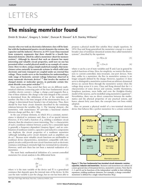
More specifically, Chua noted that there are six different mathematical<br />
relations connecting pairs of the four fundamental circuit<br />
variables: electric current i, voltage v, charge q and magnetic flux Q.<br />
One of these relations (the charge is the time integral of the current)<br />
is determined from the definitions of two of the variables, and<br />
another (the flux is the time integral of the electromotive force, or<br />
voltage) is determined from Faraday’s law of induction. Thus, there<br />
should be four basic circuit elements described by the remaining<br />
relations between the variables (Fig. 1). <strong>The</strong> ‘<strong>missing</strong>’ element—the<br />
<strong>memristor</strong>, with memristance M—provides a functional relation<br />
between charge and flux, dQ 5 Mdq.<br />
In the case of linear elements, in which M is a constant, memristance<br />
is identical to resistance and, thus, is of no special interest.<br />
However, if M is itself a function of q, yielding a nonlinear circuit<br />
element, then the situation is more interesting. <strong>The</strong> i–v characteristic<br />
of such a nonlinear relation between q and Q for a sinusoidal input<br />
is generally a frequency-dependent Lissajous figure1 , and no combination<br />
of nonlinear resistive, capacitive and inductive components<br />
can duplicate the circuit properties of a nonlinear <strong>memristor</strong><br />
(although including active circuit elements such as amplifiers can<br />
do so) 1 . Because most valuable circuit functions are attributable to<br />
nonlinear device characteristics, <strong>memristor</strong>s compatible with integrated<br />
circuits could provide new circuit functions such as electronic<br />
resistance switching at extremely high two-terminal device densities.<br />
However, until now there has not been a material realization of a<br />
<strong>memristor</strong>.<br />
<strong>The</strong> most basic mathematical definition of a current-controlled<br />
<strong>memristor</strong> for circuit analysis is the differential form<br />
v~R(w)i ð1Þ<br />
dw<br />
~i ð2Þ<br />
dt<br />
where w is the state variable of the device and R is a generalized<br />
resistance that depends upon the internal state of the device. In this<br />
case the state variable is just the charge, but no one has been able to<br />
1 HP Labs, 1501 Page Mill Road, Palo Alto, California 94304, USA.<br />
80<br />
©2008<br />
propose a physical model that satisfies these simple equations. In<br />
1976 Chua and Kang generalized the <strong>memristor</strong> concept to a much<br />
broader class of nonlinear dynamical systems they called memristive<br />
systems23 , described by the equations<br />
v~R(w,i)i ð3Þ<br />
dw<br />
~f (w,i) ð4Þ<br />
dt<br />
where w can be a set of state variables and R and f can in general be<br />
explicit functions of time. Here, for simplicity, we restrict the discussion<br />
to current-controlled, time-invariant, one-port devices. Note<br />
that, unlike in a <strong>memristor</strong>, the flux in memristive systems is no<br />
longer uniquely defined by the charge. However, equation (3) does<br />
serve to distinguish a memristive system from an arbitrary dynamical<br />
device; no current flows through the memristive system when the<br />
voltage drop across it is zero. Chua and Kang showed that the i–v<br />
characteristics of some devices and systems, notably thermistors,<br />
Josephson junctions, neon bulbs and even the Hodgkin–Huxley<br />
model of the neuron, can be modelled using memristive equations23 .<br />
Nevertheless, there was no direct connection between the mathematics<br />
and the physical properties of any practical system, and<br />
hence, almost forty years later, the concepts have not been widely<br />
adopted.<br />
Here we present a physical model of a two-terminal electrical<br />
device that behaves like a perfect <strong>memristor</strong> for a certain restricted<br />
i<br />
Resistor<br />
dv = Rdi<br />
Inductor<br />
dj = Ldi<br />
Vol 453 | 1 May 2008 | doi:10.1038/nature06932<br />
v<br />
dj = vdt<br />
j<br />
Capacitor<br />
dq = Cdv<br />
dq = idt<br />
Memristor<br />
dj = Mdq<br />
q<br />
Memristive systems<br />
Figure 1 | <strong>The</strong> four fundamental two-terminal circuit elements: resistor,<br />
capacitor, inductor and <strong>memristor</strong>. Resistors and <strong>memristor</strong>s are subsets of<br />
a more general class of dynamical devices, memristive systems. Note that R,<br />
C, L and M can be functions of the independent variable in their defining<br />
equations, yielding nonlinear elements. For example, a charge-controlled<br />
<strong>memristor</strong> is defined by a single-valued function M(q).<br />
Nature Publishing Group
NATURE | Vol 453 | 1 May 2008 LETTERS<br />
range of the state variable w and as a memristive system for another,<br />
wider (but still bounded), range of w. This intuitive model produces<br />
rich hysteretic behaviour controlled by the intrinsic nonlinearity of<br />
M and the boundary conditions on the state variable w. <strong>The</strong> results<br />
provide a simplified explanation for reports of current–voltage<br />
anomalies, including switching and hysteretic conductance, multiple<br />
conductance states and apparent negative differential resistance,<br />
especially in thin-film, two-terminal nanoscale devices, that have<br />
been appearing in the literature for nearly 50 years 2–4 .<br />
Electrical switching in thin-film devices has recently attracted<br />
renewed attention, because such a technology may enable functional<br />
scaling of logic and memory circuits well beyond the limits of complementary<br />
metal–oxide–semiconductors 24,25 . <strong>The</strong> microscopic<br />
nature of resistance switching and charge transport in such devices<br />
is still under debate, but one proposal is that the hysteresis<br />
requires some sort of atomic rearrangement that modulates the<br />
electronic current. On the basis of this proposition, we consider a<br />
thin semiconductor film of thickness D sandwiched between two<br />
metal contacts, as shown in Fig. 2a. <strong>The</strong> total resistance of the<br />
device is determined by two variable resistors connected in series<br />
(Fig. 2a), where the resistances are given for the full length D of<br />
the device. Specifically, the semiconductor film has a region with a<br />
high concentration of dopants (in this example assumed to be positive<br />
ions) having low resistance RON, and the remainder has a low<br />
(essentially zero) dopant concentration and much higher resistance<br />
ROFF.<br />
<strong>The</strong> application of an external bias v(t) across the device will move<br />
the boundary between the two regions by causing the charged<br />
dopants to drift 26 . For the simplest case of ohmic electronic conduction<br />
and linear ionic drift in a uniform field with average ion mobility<br />
mV, we obtain<br />
a b<br />
c<br />
V<br />
Undoped:<br />
Doped:<br />
w<br />
Doped<br />
D<br />
Undoped<br />
A<br />
OFF<br />
ON<br />
ON wID OFF wID<br />
Voltage<br />
w/D<br />
1.0<br />
0.5<br />
0.0<br />
–0.5<br />
–1.0<br />
1.0<br />
0.5<br />
0.0<br />
10<br />
5<br />
0<br />
–5<br />
–10<br />
0.0<br />
Charge<br />
0.1<br />
0.6<br />
0.4<br />
0.2<br />
0.0<br />
0<br />
0.2 0.3 0.4<br />
Time (×103 )<br />
50<br />
Flux<br />
w 0<br />
w(t)<br />
v(t)~ RON<br />
D zROFF 1{ w(t)<br />
D<br />
i(t) ð5Þ<br />
dw(t)<br />
dt ~m RON<br />
V i(t) ð6Þ<br />
D<br />
which yields the following formula for w(t):<br />
RON<br />
w(t)~mV q(t) ð7Þ<br />
D<br />
By inserting equation (7) into equation (5) we obtain the memristance<br />
of this system, which for RON=ROFF simplifies to:<br />
M(q)~ROFF 1{ mVRON D2 q(t)<br />
<strong>The</strong> q-dependent term in parentheses on the right-hand side of this<br />
equation is the crucial contribution to the memristance, and it<br />
becomes larger in absolute value for higher dopant mobilities mV<br />
and smaller semiconductor film thicknesses D. For any material, this<br />
term is 1,000,000 times larger in absolute value at the nanometre scale<br />
than it is at the micrometre scale, because of the factor of 1/D 2 , and<br />
the memristance is correspondingly more significant. Thus, memristance<br />
becomes more important for understanding the electronic<br />
characteristics of any device as the critical dimensions shrink to the<br />
nanometre scale.<br />
<strong>The</strong> coupled equations of motion for the charged dopants and the<br />
electrons in this system take the normal form for a current-controlled<br />
(or charge-controlled) <strong>memristor</strong> (equations (1) and (2)). <strong>The</strong><br />
fact that the magnetic field does not play an explicit role in the<br />
0.5<br />
10 w 0<br />
–1.0 –0.5 0.0 0.5 1.0<br />
Voltage<br />
Figure 2 | <strong>The</strong> coupled variable-resistor model for a <strong>memristor</strong>. a, Diagram<br />
with a simplified equivalent circuit. V, voltmeter; A, ammeter. b, c, <strong>The</strong><br />
applied voltage (blue) and resulting current (green) as a function of time t for<br />
a typical <strong>memristor</strong>. In b the applied voltage is v0sin(v0t) and the resistance<br />
ratio is ROFF=RON~160, and in c the applied voltage is 6v0sin 2 (v0t) and<br />
ROFF=RON~380, where v0 is the magnitude of the applied voltage and v0 is<br />
the frequency. <strong>The</strong> numbers 1–6 label successive waves in the applied voltage<br />
and the corresponding loops in the i–v curves. In each plot the axes are<br />
dimensionless, with voltage, current, time, flux and charge expressed in units<br />
of v0 5 1V,i0:v0=RON~10 mA, t0 ; 2p/v0 ; D 2 /mVv0 5 10 ms, v0t0 and<br />
Current (×10 –3 )<br />
©2008<br />
0.6<br />
Nature Publishing Group<br />
10<br />
5<br />
0<br />
–5<br />
–10<br />
Current (×10 –3 )<br />
Voltage<br />
w/D<br />
1.0<br />
0.5<br />
0.0<br />
–0.5<br />
–1.0<br />
1.0<br />
Current (×10 –3 )<br />
0.5<br />
0.0<br />
–4<br />
–8<br />
0.0<br />
8<br />
4<br />
0<br />
Charge<br />
6<br />
5<br />
1 2 3<br />
0.1<br />
0.6<br />
0.4<br />
0.2<br />
0.0<br />
0<br />
4<br />
0.2<br />
100<br />
Flux<br />
0.3 0.4<br />
Time (×103 )<br />
4 5 6<br />
0.5<br />
–1.0 –0.5 0.0 0.5 1.0<br />
Voltage<br />
i 0t 0, respectively. Here i 0 denotes the maximum possible current through the<br />
device, and t0 is the shortest time required for linear drift of dopants across<br />
the full device length in a uniform field v0/D, for example with D 5 10 nm<br />
and mV 5 10 210 cm 2 s 21 V 21 . We note that, for the parameters chosen, the<br />
applied bias never forces either of the two resistive regions to collapse; for<br />
example, w/D does not approach zero or one (shown with dashed lines in the<br />
middle plots in b and c). Also, the dashed i–v plot in b demonstrates the<br />
hysteresis collapse observed with a tenfold increase in sweep frequency. <strong>The</strong><br />
insets in the i–v plots in b and c show that for these examples the charge is a<br />
single-valued function of the flux, as it must be in a <strong>memristor</strong>.<br />
3<br />
0.6<br />
2<br />
1<br />
8<br />
4<br />
0<br />
–4<br />
–8<br />
Current (×10 –3 )<br />
81
LETTERS NATURE | Vol 453 |1 May 2008<br />
mechanism of memristance is one possible reason why the phenomenon<br />
has been hidden for so long; those interested in memristive<br />
devices were searching in the wrong places. <strong>The</strong> mathematics simply<br />
require there to be a nonlinear relationship between the integrals of<br />
the current and voltage, which is realized in equations (5) and (6).<br />
Another significant issue that was not anticipated by Chua is that the<br />
state variable w, which in this case specifies the distribution of<br />
dopants in the device, is bounded between zero and D. <strong>The</strong> state<br />
variable is proportional to the charge q that passes through the<br />
device until its value approaches D; this is the condition of ‘hard’<br />
switching (large voltage excursions or long times under bias). As long<br />
as the system remains in the <strong>memristor</strong> regime, any symmetrical<br />
alternating-current voltage bias results in double-loop i–v hysteresis<br />
that collapses to a straight line for high frequencies (Fig. 2b). Multiple<br />
continuous states will also be obtained if there is any sort of asymmetry<br />
in the applied bias (Fig. 2c).<br />
Obviously, equation (7) is only valid for values of w in the interval<br />
[0, D]. Different hard-switching cases are defined by imposing a variety<br />
of boundary conditions, such as assuming that once the value of w<br />
reaches either of the boundaries, it remains constant until the voltage<br />
reverses polarity. In such a case, the device satisfies the normal equations<br />
for a current-controlled memristive system (equations (3) and<br />
(4)). Figure 3a, b shows two qualitatively different i–v curves that are<br />
possible for such a memristive device. In Fig. 3a, the upper boundary<br />
is reached while the derivative of the voltage is negative, producing an<br />
apparent or ‘dynamical’ negative differential resistance. Unlike a true<br />
‘static’ negative differential resistance, which would be insensitive to<br />
time and device history, such a dynamical effect is simply a result of<br />
the charge-dependent change in the device resistance, and can be<br />
identified by a strong dependence on the frequency of a sinusoidal<br />
driving voltage. In another case, for example when the boundary is<br />
reached much faster by doubling the magnitude of the applied voltage<br />
(Fig. 3b), the switching event is a monotonic function of current.<br />
Even though in the hard-switching case there appears to be a clearly<br />
defined threshold voltage for switching from the ‘off’ (high resistance)<br />
state to the ‘on’ (low resistance) state, the effect is actually<br />
dynamical. This means that any positive voltage v1 applied to the<br />
device in the off state will eventually switch it to the on state after time<br />
*D 2 ROFF=(2m VvzRON). <strong>The</strong> device will remain in the on state as<br />
long as a positive voltage is applied, but even a small negative bias will<br />
switch it back to the off state; this is why a current-hysteresis loop is<br />
only observed for the positive voltage sweep in Fig. 3a, b.<br />
In nanoscale devices, small voltages can yield enormous electric<br />
fields, which in turn can produce significant nonlinearities in ionic<br />
transport. Figure 3c illustrates such a case in which the right-hand<br />
side of equation (6) is multiplied by a window function w(1 2 w)/D 2 ,<br />
which corresponds to nonlinear drift when w is close to zero or D.In<br />
this case, the switching event requires a significantly larger amount of<br />
charge (or even a threshold voltage) in order for w to approach either<br />
boundary. <strong>The</strong>refore, the switching is essentially binary because the<br />
on and off states can be held much longer if the voltage does not<br />
exceed a specific threshold. Nonlinearity can also be expected in the<br />
electronic transport, which can be due to, for example, tunnelling at<br />
the interfaces or high-field electron hopping. In this case, the hysteresis<br />
behaviour discussed above remains essentially the same but the<br />
i–v characteristic becomes nonlinear.<br />
<strong>The</strong> model of equations (5) and (6) exhibits many features that<br />
have been described as bipolar switching, that is, when voltages of<br />
opposite polarity are required for switching a device to the on state<br />
and the off state. This type of behaviour has been experimentally<br />
observed in various material systems: organic films 5–9 that contain<br />
charged dopants or molecules with mobile charged components;<br />
chalcogenides 4,10–12 , where switching is attributed to ion migration<br />
rather than a phase transition; and metal oxides 2–4,20 , notably TiO2<br />
(refs 4, 13, 14, 21) and various perovskites 4,15–19 . For example, multistate<br />
8–14,16–18,20,21 and binary 3,4,7,15,16 switching that are similar to those<br />
modelled in Figs 2c and 3c, respectively, have been observed, with<br />
some showing dynamical negative differential resistance. Typically,<br />
hysteresis such as in Fig. 3c is observed for both voltage polarities<br />
7,9–12,14–17,21 , but observations of i–v characteristics resembling<br />
Fig. 3a, b have also been reported 8,17–20 . In our own studies of TiOx<br />
devices, i–v behaviours very similar to those in Figs 2b, 2c and 3c are<br />
regularly observed. Figure 3d illustrates an experimental i–v characteristic<br />
from a metal/oxide/metal cross-point device within which<br />
the critical 5-nm-thick oxide film initially contained one layer of<br />
insulating TiO2 and one layer of oxygen-poor TiO22x (refs 21, 22).<br />
In this system, oxygen vacancies act as mobile 12-charged dopants,<br />
which drift in the applied electric field, shifting the dividing line<br />
between the TiO2 and TiO22x layers. <strong>The</strong> switching characteristic<br />
observed for a particular memristive system helps classify the nature<br />
of the boundary conditions on the state variable of the device.<br />
<strong>The</strong> rich hysteretic i–v characteristics detected in many thin-film,<br />
two-terminal devices can now be understood as memristive behaviour<br />
defined by coupled equations of motion: some for (ionized)<br />
atomic degrees of freedom that define the internal state of the device,<br />
and others for the electronic transport. This behaviour is increasingly<br />
relevant as the active region in many electronic devices continues to<br />
shrink to a width of only a few nanometres, so even a low applied<br />
voltage corresponds to a large electric field that can cause charged<br />
species to move. Such dopant or impurity motion through the active<br />
region can produce dramatic changes in the device resistance.<br />
Including <strong>memristor</strong>s and memristive systems in integrated circuits<br />
has the potential to significantly extend circuit functionality as long<br />
as the dynamical nature of such devices is understood and properly<br />
a b c d<br />
0.0 0.4 0.8 1.2 1.6<br />
1<br />
1.0<br />
0<br />
0.5<br />
4<br />
0.2<br />
OFF<br />
0.1<br />
–1<br />
0.0 0.4 0.8<br />
1.0<br />
0.5<br />
0.0<br />
1.2<br />
0.0<br />
1.6<br />
2<br />
0<br />
–2<br />
/ Time (×10<br />
0.0 0.1 0.2 0.3 0.4<br />
1<br />
1.0<br />
0<br />
0.5<br />
–1<br />
0.0 0.1 0.2<br />
ON = 125<br />
v0 = 1 V<br />
0.3<br />
0.0<br />
0.4<br />
3 )<br />
Time (×10<br />
0.0 0.2 0.4 0.6 0.8<br />
1<br />
1.0<br />
0<br />
0.5<br />
–1<br />
0.0 0.2 0.4<br />
1.0<br />
0.5<br />
0.6<br />
0.0<br />
0.8<br />
3 ) Time (×103 )<br />
OFF / ON = 50 OFF / v0 = 2 V<br />
ON = 50<br />
v0 = 4 V<br />
Voltage<br />
Current<br />
0.0<br />
–1.0 –0.5 0.0 0.5 1.0<br />
Voltage<br />
w/D<br />
0.0<br />
–1.0 –0.5 0.0 0.5 1.0<br />
Voltage<br />
Figure 3 | Simulations of a voltage-driven memristive device. a, Simulation<br />
with dynamic negative differential resistance; b, simulation with no dynamic<br />
negative differential resistance; c, simulation governed by nonlinear ionic<br />
drift. In the upper plots of a, b and c we plot the voltage stimulus (blue) and<br />
the corresponding change in the normalized state variable w/D (red), versus<br />
82<br />
Current Voltage<br />
©2008<br />
w/D<br />
Current<br />
Voltage<br />
–0.5<br />
–1.0<br />
–1.0 –0.5 0.0 0.5 1.0<br />
Voltage<br />
w/D<br />
Current (mA)<br />
–4<br />
Pt<br />
TiO2 Pt<br />
–1.0 0.0 1.0<br />
Voltage (V)<br />
time. In all cases, hard switching occurs when w/D closely approaches the<br />
boundaries at zero and one (dashed), and the qualitatively different i–v<br />
hysteresis shapes are due to the specific dependence of w/D on the electric<br />
field near the boundaries. d, For comparison, we present an experimental i–v<br />
plot of a Pt–TiO22x–Pt device 21 .<br />
Nature Publishing Group
NATURE | Vol 453 | 1 May 2008 LETTERS<br />
used. Important applications include ultradense, semi-non-volatile<br />
memories and learning networks that require a synapse-like<br />
function.<br />
Received 6 December 2007; accepted 17 March 2008.<br />
1. Chua, L. O. Memristor - the <strong>missing</strong> circuit element. IEEE Trans. Circuit <strong>The</strong>ory 18,<br />
507–519 (1971).<br />
2. Hickmott, M. T. Low-frequency negative resistance in thin anodic oxide films.<br />
J. Appl. Phys. 33, 2669–2682 (1962).<br />
3. Dearnaley, G., Stoneham, A. M. & Morgan, D. V. Electrical phenomena in<br />
amorphous oxide films. Rep. Prog. Phys. 33, 1129–1192 (1970).<br />
4. Waser, R. & Aono, M. Nanoionics-based resistive switching memories. Nature<br />
Mater. 6, 833–840 (2007).<br />
5. Scott, J. C. & Bozano, L. D. Nonvolatile memory elements based on organic<br />
materials. Adv. Mater. 19, 1452–1463 (2007).<br />
6. Collier, C. P. et al. A [2]catenane-based solid state electronically reconfigurable<br />
switch. Science 289, 1172–1175 (2000).<br />
7. Zhitenev, N. B., Sidorenko, A., Tennant, D. M. & Cirelli, R. A. Chemical modification<br />
of the electronic conducting states in polymer nanodevices. Nature Nanotechnol.<br />
2, 237–242 (2007).<br />
8. Smits, J. H. A., Meskers, S. C. J., Janssen, R. A. J., Marsman, A. W. & de Leeuw,<br />
D. M. Electrically rewritable memory cells from poly(3-hexylthiophene) Schottky<br />
diodes. Adv. Mater. 17, 1169–1173 (2005).<br />
9. Lai, Q. X., Zhu, Z. H., Chen, Y., Patil, S. & Wudl, F. Organic nonvolatile memory by<br />
dopant-configurable polymer. Appl. Phys. Lett. 88, 133515 (2006).<br />
10. Terabe, K., Hasegawa, T., Nakayama, T. & Aono, M. Quantized conductance<br />
atomic switch. Nature 433, 47–50 (2005).<br />
11. Kozicki, M. N., Park, M. & Mitkova, M. Nanoscale memory elements based on<br />
solid-state electrolytes. IEEE Trans. Nanotechnol. 4, 331–338 (2005).<br />
12. Dietrich, S. et al. A nonvolatile 2-Mbit CBRAM memory core featuring advanced<br />
read and program control. IEEE J. Solid State Circuits 42, 839–845 (2007).<br />
13. Jameson, J. R. et al. Field-programmable rectification in rutile TiO2 crystals. Appl.<br />
Phys. Lett. 91, 112101 (2007).<br />
14. Jeong, D. S., Schroeder, H. & Waser, R. Coexistence of bipolar and unipolar<br />
resistive switching behaviors in a Pt/TiO 2/Pt stack. Electrochem. Solid State Lett.<br />
10, G51–G53 (2007).<br />
©2008<br />
Nature Publishing Group<br />
15. Beck, A., Bednorz, J. G., Gerber, C., Rossel, C. & Widmer, D. Reproducible<br />
switching effect in thin oxide films for memory applications. Appl. Phys. Lett. 77,<br />
139–141 (2000).<br />
16. Szot, K., Speier, W., Bihlmayer, G. & Waser, R. Switching the electrical resistance<br />
of individual dislocations in single-crystalline SrTiO3. Nature Mater. 5, 312–320<br />
(2006).<br />
17. Sawa, A., Fujii, T., Kawasaki, M. & Tokura, Y. Interface resistance switching at a<br />
few nanometer thick perovskite manganite active layers. Appl. Phys. Lett. 88,<br />
232112 (2006).<br />
18. Hamaguchi, M., Aoyama, K., Asanuma, S., Uesu, Y. & Katsufuji, T. Electric-fieldinduced<br />
resistance switching universally observed in transition-metal-oxide thin<br />
films. Appl. Phys. Lett. 88, 142508 (2006).<br />
19. Oligschlaeger, R., Waser, R., Meyer, R., Karthauser, S. & Dittmann, R. Resistive<br />
switching and data reliability of epitaxial (Ba,Sr)TiO3 thin films. Appl. Phys. Lett.<br />
88, 042901 (2006).<br />
20. Richter, C. A., Stewart, D. R., Ohlberg, D. A. A. & Williams, R. S. Electrical<br />
characterization of Al/AlOx/molecule/Ti/Al devices. Appl. Phys. Mater. Sci.<br />
Process. 80, 1355–1362 (2005).<br />
21. Stewart, D. R. et al. Molecule-independent electrical switching in Pt/organic<br />
monolayer/Ti devices. Nano Lett. 4, 133–136 (2004).<br />
22. Blackstock, J. J., Stickle, W. F., Donley, C. L., Stewart, D. R. & Williams, R. S. Internal<br />
structure of a molecular junction device: chemical reduction of PtO2 by Ti<br />
evaporation onto an interceding organic monolayer. J. Phys. Chem. C 111, 16–20<br />
(2007).<br />
23. Chua, L. O. & Kang, S. M. Memristive devices and systems. Proc. IEEE 64, 209–223<br />
(1976).<br />
24. Kuekes, P. J., Snider, G. S. & Williams, R. S. Crossbar nanocomputers. Sci. Am. 293,<br />
72–78 (2005).<br />
25. Strukov, D. B. & Likharev, K. K. Defect-tolerant architectures for nanoelectronic<br />
crossbar memories. J. Nanosci. Nanotechnol. 7, 151–167 (2007).<br />
26. Blanc, J. & Staebler, D. L. Electrocoloration in SrTiO - vacancy drift and oxidationreduction<br />
of transition metals. Phys. Rev. B 4, 3548–3557 (1971).<br />
Acknowledgements This research was conducted with partial support from<br />
DARPA and DTO.<br />
Author Information Reprints and permissions information is available at<br />
www.nature.com/reprints. Correspondence and requests for materials should be<br />
addressed to R.S.W. (stan.williams@hp.com).<br />
83