download PDF - Ropla Elektronik Sp. z oo
download PDF - Ropla Elektronik Sp. z oo
download PDF - Ropla Elektronik Sp. z oo

You also want an ePaper? Increase the reach of your titles
YUMPU automatically turns print PDFs into web optimized ePapers that Google loves.
www.passivecomponent.com<br />
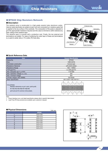
■ WT04X Chip Resistors Network<br />
■ Description<br />
The resistors array is constructed in a high grade ceramic body (aluminum oxide).<br />
Internal metal electrodes are added at each end and connected by a resistive paste that<br />
is applied to the top surface of the substrate. The composition of the paste is adjusted to<br />
give the approximate resistance required and the value is trimmed to within tolerance by<br />
laser cutting of this resistive layer.<br />
The resistive layer is covered with a protective coat. Finally, the two external end<br />
terminations are added. For ease of soldering the outer layer of these end terminations<br />
is a Lead-tin solder alloy or Tin solder (Pb free) alloy.<br />
■ Quick Reference Data<br />
Item General <strong>Sp</strong>ecification<br />
Series No. WT04X<br />
Size 1206 (3216)<br />
Terminaton construction Convex type<br />
Resistance Tolerance ±5% (E24 series)<br />
Resistance Range 10Ω ~ 100KΩ<br />
TCR (ppm/ºC) ≤ ± 200 ppm/ºC<br />
Max. dissipation @ Tamb=70ºC 1/16 Watt<br />
Max. Operation Voltage (DC or RMS) 25V<br />
Max. Overload Voltage 50V<br />
Climatic category (IEC 60068) 55/155/56<br />
Basic <strong>Sp</strong>ecification JIS C 5201-1/IEC 60115-1<br />
Circuit Mode<br />
Resistor elements on pin1~pin4, pin6~pin9;<br />
R1=R2=R3=R4=R6=R7=R8=R9<br />
pin5 and pin10 common (Grounded).<br />
Note :<br />
1. Power derating curve, and detail specification please refer to specific data sheets.<br />
2. Lead Free (Pb free) products are available upon customer’s request.<br />
■ Physical Dimensions<br />
WT04X<br />
L 3.30 ± 0.20<br />
W 1.60 ± 0.15<br />
T 0.55 ± 0.10<br />
P 0.64 ± 0.05<br />
A 0.50 ± 0.05<br />
B 0.40 ± 0.15<br />
C 0.40 ± 0.15<br />
G 0.40 ± 0.15<br />
Chip Resistors<br />
Unit: mm<br />
Marking<br />
Inner Electrode<br />
Resistor<br />
10 9 8 7 6<br />
1 2 3 4 5<br />
W<br />
B<br />
P<br />
A<br />
Protective Coat<br />
Laser Trimming<br />
L C<br />
T<br />
G<br />
Termination<br />
10 11