download PDF - Ropla Elektronik Sp. z oo
download PDF - Ropla Elektronik Sp. z oo
download PDF - Ropla Elektronik Sp. z oo

Create successful ePaper yourself
Turn your PDF publications into a flip-book with our unique Google optimized e-Paper software.
www.passivecomponent.com<br />
INDEX<br />
Subject Page<br />
How to Order . . . . . . . . . . . . . . . . . . . . . . . . . . . . . . . . . . . . . . . . . . . . . . . . . . . . . 1<br />
Chip Resistors Selection Guide. . . . . . . . . . . . . . . . . . . . . . . . . . . . . . . . . . . . 2~3<br />
General Purpose Chip Resistors (1Ω~10MΩ) . . . . . . . . . . . . . . . . . . . . . . . . . . . 4<br />
Low Ohmic Chip Resistors (0.02Ω~1Ω). . . . . . . . . . . . . . . . . . . . . . . . . . . . . . . . 5<br />
Ultra Low Ohmic Sensing Chip Resistors (0.001Ω~0.025Ω) . . . . . . . . . . . . . . . 6<br />
Chip Resistors Array : Convex Termination . . . . . . . . . . . . . . . . . . . . . . . . . . . . 7<br />
WA06W Chip Resistors Array 16P8R . . . . . . . . . . . . . . . . . . . . . . . . . . . . . . . . . 8<br />
Chip Resistors Array : Concave Termination . . . . . . . . . . . . . . . . . . . . . . . . . . . 9<br />
WT04X Chip Resistors Network . . . . . . . . . . . . . . . . . . . . . . . . . . . . . . . . . . . . 10<br />
WA04P Chip Attenuator . . . . . . . . . . . . . . . . . . . . . . . . . . . . . . . . . . . . . . . . . . . 11<br />
<strong>Sp</strong>ecial Chip Resistors . . . . . . . . . . . . . . . . . . . . . . . . . . . . . . . . . . . . . . . . . . . . 12<br />
WFxxY Series of Gold Terminations . . . . . . . . . . . . . . . . . . . . . . . . . . . . . . . . . 12<br />
WFxxG Series of High Ohmic Chip Resistors . . . . . . . . . . . . . . . . . . . . . . . . . 12<br />
WFxxM Series of Trimmable Chip Resistors . . . . . . . . . . . . . . . . . . . . . . . . . . 13<br />
WFxxV Series of High Voltage Chip Resistors . . . . . . . . . . . . . . . . . . . . . . . . . 13<br />
WFxxP/WWxxP Series of High Power Chip Resistors . . . . . . . . . . . . . . . . . . . 14<br />
WFxxS Series of Surge Chip Resistors. . . . . . . . . . . . . . . . . . . . . . . . . . . . . . . 15<br />
Precision Chip Resistors . . . . . . . . . . . . . . . . . . . . . . . . . . . . . . . . . . . . . . . . . . 15<br />
Test and Requirements . . . . . . . . . . . . . . . . . . . . . . . . . . . . . . . . . . . . . . . . . . . . 16<br />
Packing on Tape and Reel . . . . . . . . . . . . . . . . . . . . . . . . . . . . . . . . . . . . . . . . . 17<br />
F<strong>oo</strong>tprint Design . . . . . . . . . . . . . . . . . . . . . . . . . . . . . . . . . . . . . . . . . . . . . . . . . 18<br />
Storage and Handling Condition . . . . . . . . . . . . . . . . . . . . . . . . . . . . . . . . . . . . 19<br />
Recommendation of Soldering Profile . . . . . . . . . . . . . . . . . . . . . . . . . . . . . . . 19
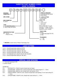
■ HOW TO ORDER<br />
12<br />
Chip Resistors<br />
Remark: 1. Detail product part number, functional code, tolerance combination,...please refer to specific data sheet.<br />
2. Example: (“_” means blank)<br />
Chip-R 0805 size, 4.3ohm, 5% Normal type, SnPb termination, 5000pcs taped in reel: WR08X4R3_JT_<br />
Chip-R 0805 size, 4.3ohm, 5% Normal type, Sn Lead free termination, 5000pcs taped in reel: WR08X4R3_JTL<br />
Chip-R 0603 size, 100ohm, 5% Normal type, SnPb termination, 5000pcs taped in reel: WR06X101_JT_<br />
Chip-R 0603 size, 100ohm, 1% Normal type, Sn termination, 5000pcs taped in reel: WR06X1000FTL<br />
Low ohmic Chip-R 2512 size, 0.1ohm, 1% Normal type, SnPb termination, 4000pcs taped in reel: WW25XR100FT_<br />
Low ohmic Chip-R 2512 size, 0.1ohm, 1% Normal type, Sn Lead free termination, 4000pcs taped in reel: WW25XR100FTL<br />
Chip-R array 0603x4, 10Kohm, 5% convex with SnPb termination, 5000pcs taped in reel: WA06X103_JT_<br />
Chip-R 0402 size, 220ohm, Normal type, Gold termination, 5% 10,000pcs taped in reel: WF04Y221_JTG<br />
Chip-R 0603 size, 0ohm, Normal type, SnPb termination, 5000pcs taped in reel: WR06X000_PT_<br />
www.passivecomponent.com<br />
WR 06 X 1000 F T L<br />
Type code<br />
R: Discrete<br />
1~10MR<br />
Size code<br />
25 : 2512 (6432)<br />
20 : 2010 (5025)<br />
18 : 1218 (3248)<br />
12 : 1206 (3216)<br />
10 : 1210 (3225)<br />
06 : 0603 (1608)<br />
08 : 0805 (2012)<br />
04 : 0402 (1005)<br />
02 : 0201 (0603)<br />
Functional code<br />
X : Normal<br />
W : 1% for1Mohm<br />
Resistance<br />
E24(J tol.) : 2 significant digits<br />
followd by No. of<br />
zeros and a blank<br />
e.g. : 3ohm=3R0_<br />
10ohm=100_<br />
220ohm=221_<br />
56Kohm=563_<br />
(“_” means blank)<br />
E24,E96(F tol.) : 3 significant<br />
digits followd by No. of<br />
zeros<br />
Tolerance<br />
F : +/- 1%<br />
J : +/- 5%<br />
P : Jumper<br />
Packaging code<br />
P : 4” reel taping<br />
T : 7” reel taping<br />
A : 7” reel taping 15Kpcs<br />
Q : 10” reel taping<br />
G : 13” reel taping<br />
R : 0603 2mm pitch taping<br />
B : Bulk<br />
K : Bulkcase<br />
Termination code<br />
_ = SnPb base<br />
(“_” means blank)<br />
L = Sn base (Lead free)<br />
R = Pb ≤ 100 ppm<br />
(total)<br />
WW 25 M R002 F T L<br />
Type code<br />
R: < 1ohm<br />
Size code<br />
25 : 2512 (6432)<br />
20 : 2010 (5025)<br />
18 : 1218 (3248)<br />
12 : 1206 (3216)<br />
10 : 1210 (3225)<br />
08 : 0805 (2012)<br />
06 : 0603 (1608)<br />
04 : 0402 (1005)<br />
Functional code<br />
X : Normal<br />
M : Sensing type<br />
N : Sensing type, High Power<br />
W : Thick film low TCR type<br />
F : Metal Foil<br />
P : Power ( 2512 size=2 watt,<br />
2010 size=0.75 watt,<br />
1210 size=0.5 watt,<br />
1206 size=0.5 watt,<br />
0805 size=0.25 watt,<br />
0603 size=0.125 watt )<br />
Resistance<br />
“R” followed by 3<br />
significant digits<br />
e.g. :<br />
0.1ohm=R100<br />
0.033ohm=R033<br />
0.56ohm=R560<br />
Tolerance<br />
F : +/- 1%<br />
G : +/- 2%<br />
J : +/- 5%<br />
Packaging code<br />
P : 4” reel taping<br />
T : 7” reel taping<br />
Q : 10” reel taping<br />
G : 13” reel taping<br />
R : 0603 2mm pitch taping<br />
B : Bulk<br />
K : Bulkcase<br />
Termination code<br />
_ = SnPb base<br />
(“_” means blank)<br />
L = Sn base (Lead free)<br />
G = Au base<br />
S = Ag base<br />
WF 04 H 1001 B T L<br />
Type code<br />
F: <strong>Sp</strong>ecial<br />
function<br />
Size code<br />
25 : 2512 (6432)<br />
20 : 2010 (5025)<br />
18 : 1218 (3248)<br />
12 : 1206 (3216)<br />
10 : 1210 (3225)<br />
08 : 0805 (2012)<br />
06 : 0603 (1608)<br />
04 : 0402 (1005)<br />
Functional code<br />
G : High ohmic (>10Mohm)<br />
H : Thick film, Precision<br />
toleranceWR and WW series)<br />
S : Surge<br />
T : Thin film, TCR50ppm<br />
U : Thin film, TCR25ppm<br />
V : High voltage<br />
X : <strong>Sp</strong>ecial resistance<br />
Y : E24/E96 resistance with<br />
special termination (non<br />
SnPb or Sn base), ≥1%<br />
Resistance<br />
E24(J tol.) : 2 significant digits<br />
followd by No. of<br />
zeros and a blank<br />
e.g. : 3ohm=3R0_<br />
10ohm=100_<br />
220ohm=221_<br />
56Kohm=563_<br />
(“_” means blank)<br />
E24,E96(F tol.) : 3 significant<br />
digits followd by No. of<br />
zeros<br />
Tolerance<br />
B : +/- 0.1%<br />
C : +/- 0.25%<br />
D : +/- 0.5%<br />
F : +/- 1%<br />
G : +/- 2%<br />
J : +/- 5%<br />
K : +/- 10%<br />
L : +/- 15%<br />
M : +/- 20%<br />
P : Jumper<br />
Packaging code<br />
P : 4” reel taping<br />
T : 7” reel taping<br />
Q : 10” reel taping<br />
G : 13” reel taping<br />
R : 0603 2mm pitch taping<br />
B : Bulk<br />
K : Bulkcase<br />
Termination code<br />
_ = SnPb base<br />
(“_” means blank)<br />
L = Sn base (Lead free)<br />
G = Au base<br />
S = Ag base<br />
WA 04 Y 103_ J T L<br />
Type code<br />
A: Isolated<br />
Resistor<br />
Array<br />
Size code<br />
06 : 0603 (1608)<br />
04 : 0402 (1005)<br />
Functional code<br />
X : *4, convex<br />
Y : *2, convex<br />
W : *8, convex<br />
T : *4, concave<br />
U : *2, concave<br />
P : *3, convex (Attenuator)<br />
Resistance<br />
E24(J tol.) : 2 significant digits<br />
followd by No. of<br />
zeros and a blank<br />
e.g. : 3ohm=3R0_<br />
10ohm=100_<br />
220ohm=221_<br />
56Kohm=563_<br />
(“_” means blank)<br />
E24,E96(F tol.) : 3 significant<br />
digits followd by No. of<br />
zeros<br />
Tolerance<br />
F : +/- 1%<br />
J : +/- 5%<br />
P : Jumper<br />
Packaging code<br />
T : 7” reel taping<br />
Q : 10” reel taping<br />
G : 13” reel taping<br />
B : Bulk<br />
K : Bulkcase<br />
Termination code<br />
_ = SnPb base<br />
(“_” means blank)<br />
L = Sn base (Lead free)<br />
WT 04 X 103_ J T L<br />
Type code<br />
T: Network<br />
Resistors<br />
Size code<br />
04 : total package<br />
size 1206<br />
(3216)<br />
Functional code<br />
X : *8, convex<br />
Resistance<br />
E24(J tol.) : 2 significant digits<br />
followd by No. of<br />
zeros and a blank<br />
e.g. : 3ohm=3R0_<br />
10ohm=100_<br />
220ohm=221_<br />
56Kohm=563_<br />
(“_” means blank)<br />
E24,E96(F tol.) : 3 significant<br />
digits followd by No. of<br />
zeros<br />
Tolerance<br />
J : +/- 5%<br />
Packaging code<br />
T : 7” reel taping<br />
B : Bulk<br />
Termination code<br />
_ = SnPb base<br />
(“_” means blank)<br />
L = Sn base (Lead free)
www.passivecomponent.com<br />
■ Chip Resistors Selection Guide<br />
■ General Purpose Chip-R<br />
Chip Resistors<br />
Series Size Rated Power TCR (ppm/ºC) Tolerance Resistance<br />
WR02X 0201 (0603) 1/20W<br />
WR04X 0402 (1005) 1/16W<br />
WR06X 0603 (1608) 1/10W<br />
WR08X 0805 (2012) 1/8W<br />
WR12X 1206 (3216) 1/4W<br />
WR10X 1210 (3225) 1/3W<br />
WR18X 1218 (3248) 1W<br />
WR20X 2010 (5025) 1/2W<br />
WR25X 2512 (6432) 1W<br />
300* ±1% 10Ω ~ 1MΩ<br />
300* ±5% 1Ω ~ 10MΩ<br />
200 ±1%<br />
200* ±5%<br />
100 ±1%<br />
200 ±5%<br />
100 ±1%<br />
200 ±5%<br />
100 ±1%<br />
200<br />
200<br />
±5%<br />
±1%<br />
1Ω ~ 10MΩ<br />
200 ±5%<br />
100 ±1%<br />
100 ±5%<br />
200 ±1%<br />
200* ±5%<br />
200 ±1%<br />
200* ±5%<br />
Remark : 1. Means Detail resistance v.s. TCR and ordering code please refer to specific specifications.<br />
2. Pb free terminations upon customer requested.<br />
3. Standard junper resistors are not designed for fusing applications, designers shall apply dedicate fusible resistors or standard fuse in it`s precision circuits.<br />
■ Low Ohmic Chip-R<br />
Series Size Rated Power TCR (ppm/ºC) Tolerance Resistance<br />
WW25X 2512 (6432) 1W<br />
±1%<br />
±5%<br />
0.020Ω ~ 0.976Ω<br />
0.015Ω ~ 0.910Ω<br />
WW18X 1218 (3248) 1W<br />
≤1500**<br />
±1%<br />
±5%<br />
0.020Ω ~ 0.976Ω<br />
0.015Ω ~ 0.910Ω<br />
WW20X 2010 (5025) 1/2W<br />
±1%<br />
±5%<br />
0.020Ω ~ 0.976Ω<br />
0.015Ω ~ 0.910Ω<br />
WW10X 1210 (3225) 1/3W ≤200<br />
±1%<br />
±5%<br />
0.100Ω ~ 0.976Ω<br />
0.100Ω ~ 0.976Ω<br />
WW12X<br />
WW08X<br />
1206 (3216)<br />
0805 (2012)<br />
1/4W<br />
1/8W<br />
≤1500**<br />
≤1500**<br />
±1%, ±2%, ±5% 0.020Ω ~ 0.976Ω<br />
WW06X 0603 (1608) 1/10W ≤500** ±1%, ±2%, ±5% 0.10Ω ~ 0.976Ω<br />
WW04X 0402 (1005) 1/16W ≤600** ±1%, ±5% 0.10Ω ~ 0.976Ω<br />
Remark : 1. “**” Detail resistance v.s. TCR please refer to specification.<br />
2. Pb free terminations upon customer requested.<br />
■ Ultra Low Ohmic Sensing Chip-R<br />
Series Size Rated Power TCR (ppm/ºC) Tolerance Resistance<br />
WW25M 2512 (6432) 1W ≤100 ±1%, ±5% 0.001Ω ~ 0.025Ω<br />
WW25N 2512 (6432) 2W ≤100 ±1%, ±5% 0.001Ω ~ 0.025Ω<br />
■ Chip Resistors Array<br />
Series Size Rated Power TCR (ppm/ºC) Termination Type Tolerance Resistance<br />
WA06X 1206 (0603x4) 1/10W ≤200 Convex ±5%<br />
WA04X 0805 (0402x4) 1/16W ≤300 Convex ±5%<br />
WA04Y<br />
WA06T<br />
0404 (0402x4)<br />
1206 (0603x4)<br />
1/16W<br />
1/10W<br />
≤300<br />
≤200<br />
Convex<br />
Concave<br />
±5%<br />
±5%<br />
10Ω ~ 1MΩ<br />
WA04T 0805 (0402x4) 1/16W ≤300 Concave ±5%<br />
WA04U 0404 (0402x2) 1/16W ≤300 Concave ±5%<br />
WA06W 1606 (0602x4) 1/16W ≤200 Convex ±5% 10Ω ~ 100KΩ<br />
Remark : Pb free terminations upon customer requested.<br />
■ Chip Resistors Network<br />
Series Size Rated Power TCR (ppm/ºC) Termination Type Tolerance Resistance<br />
WT04X 1206 (10P8R) 1/16W ≤200 Convex ±5% 10Ω ~ 100KΩ<br />
Remark : Pb free terminations upon customer requested.<br />
23
■ <strong>Sp</strong>ecial Functionality Chip-R<br />
34<br />
www.passivecomponent.com<br />
Type Series Size Rated Power TCR (ppm/ºC) Tolerance Resistance<br />
Gold Termination<br />
High Ohmic<br />
Trimmable<br />
High Precision<br />
Remark : Pb free terminations upon customer requested.<br />
■ Chip Attenuator<br />
WF06Y 0603 (1608) 1/10W<br />
WF04Y 0402 (1005) 1/16W<br />
WF12G 1206 (3216) 1/4W<br />
WF08G 0805 (2012) 1/8W<br />
WF06G 0603 (1608) 1/16W<br />
WF20M 2010 (5025) 1/2W<br />
WF12M 1206 (3216) 1/4W<br />
WF08M 0805 (2012) 1/8W<br />
WF06M 0603 (1608) 1/10W<br />
WF12H 1206 (3216) 1/4W<br />
WF08H 0805 (2012) 1/8W<br />
WF06H 0603 (1608) 1/10W<br />
≤ 100 ±1% 10Ω ~ 1MΩ<br />
≤ 200 ±5% 1Ω ~ 10MΩ<br />
≤ 100 ±1% 10Ω ~ 1MΩ<br />
≤ 200 ±5% 1Ω ~ 10MΩ<br />
≤ 300 ±5% 11MΩ ~ 30MΩ<br />
≤ 200<br />
≤ 100<br />
WF04H 0402 (1005) 1/16W ≤ 200<br />
WF12T 1206 (3216) 1/8W<br />
0/-20%<br />
0/-30%<br />
±0.1%<br />
±0.5%<br />
±0.1%<br />
±0.5%<br />
1Ω ~ 10MΩ<br />
10Ω ~ 1MΩ<br />
10Ω ~ 1MΩ<br />
10Ω ~ 1MΩ<br />
WF08T 0805 (2012) 1/10W ±1%<br />
10Ω ~ 1MΩ<br />
≤ 50<br />
WF06T 0603 (1608) 1/16W ±0.5%<br />
10Ω ~ 330KΩ<br />
WF04T 0402 (1005) 1/20W 10Ω ~ 100KΩ<br />
WF12U 1206 (3216) 1/8W<br />
Chip Resistors<br />
10Ω ~ 1MΩ<br />
WF08U 0805 (2012) 1/10W ±0.1%<br />
10Ω ~ 1MΩ<br />
≤ 25<br />
WF06U 0603 (1608) 1/16W ±0.5%<br />
10Ω ~ 330KΩ<br />
WF04U 0402 (1005) 1/20W 10Ω ~ 100KΩ<br />
Series Size Type Termination Type Tolerance Attenuation Impedance<br />
WA04P 0402x2 (1005x2) 4p3R, type Convex ±0.2db ~ 1dB 1dB ~ 10dB 50Ω
www.passivecomponent.com<br />
■ General Purpose Chip Resistors (1Ω~10MΩ)<br />
■ Feature<br />
1. High reliability and stability<br />
2. Reduced size of final equipment<br />
3. Lower assembly costs<br />
4. Higher component and equipment reliability<br />
■ Description<br />
The resistors are constructed in a high grade ceramic body<br />
(aluminum oxide). Internal metal electrodes are added at each end<br />
and connected by a resistive paste that is applied to the top surface<br />
of the substrate. The composition of the paste is adjusted to give the<br />
approximate resistance required and the value is trimmed to within<br />
tolerance by laser cutting of this resistive layer.<br />
The resistive layer is covered with a protective coat. Finally, the two<br />
external end terminations are added. For ease of soldering the outer<br />
layer of these end terminations is a Lead-tin or Tin solder(Pb free)<br />
alloy.<br />
■ Quick Reference Data<br />
■ Application<br />
1. Consumer electrical equipment, PDA, Digital Camcoder, ...<br />
2. EDP, Computer application<br />
3. Mobile phone, Telecom<br />
4. Power supply, Battery charger, DC-DC power converter<br />
5. Digital meter<br />
6. Automotives<br />
Laser trimmed<br />
Resistive element<br />
Primary Layer<br />
Termination<br />
Protective Layer<br />
Marking<br />
Alumina substrate<br />
Series No. WR25X WR20X WR18X WR10X WR12X WR08X WR06X WR04X WR02X<br />
Size Code 2512 (6432) 2010 (5025) 1218(3248) 1210 (3225) 1206 (3216) 0805 (2012) 0603 (1608) 0402 (1005) 0201 (0603)<br />
Resistance Range<br />
±5% Tolerance (E24)<br />
±1% Tolerance (E24+E96)<br />
TCR (ppm/ºC)<br />
>10Ω<br />
≤10Ω<br />
≤ ± 200<br />
≤ ± 300<br />
≤ ± 100<br />
≤ ± 200<br />
1Ω~10MΩ, 0Ω<br />
1Ω~10MΩ<br />
≤ ± 100<br />
-300 ~ +500<br />
1Ω~10MΩ,0Ω<br />
10Ω~1MΩ<br />
Max. dissipation @ Tamb=70ºC 1.0 Watt 1/2 Watt 1.0 Watt 1/3 Watt 1/4 Watt 1/8 Watt 1/10 Watt 1/16 Watt 1/20 Watt<br />
Max. Operation Voltage (DC or RMS) 250V 200V 200V 200V 200V 150V 50V 50V 25V<br />
Climatic category (IEC 60068) 55/155/56 ≥55/125/56<br />
Basic <strong>Sp</strong>ecification JIS C 5201-1 / IEC 60115-1<br />
Note :<br />
1. This is the maximum voltage that may be continuously supplied to the resistor element, see “IEC publication 60115-8”<br />
2. Max. Operation Voltage : So called RCWV (Rated Continuous Working Voltage) is determined by<br />
RCWV= Rater Power x Resistance Value or Max. RCWV listed above, whichever is lower.<br />
3. Lead Free (Pb free) products are upon customer request.<br />
4. The resistance range 1 ~ 10Ω and 1M ~ 10MΩ with 1% tolerance please refer to WR12W / WR08W / WR06W / WR04W series specification.<br />
■ Physical Dimensions<br />
Unit: mm<br />
Size 2512(6432) 2010(5025) 1218(3248) 1210(3225) 1206(3216) 0805(2012) 0603(1608) 0402(1005) 0201(0603)<br />
L 6.40 ± 0.20 5.00 ± 0.20 3.05 ± 0.15 3.10 ± 0.10 3.10 ± 0.10 2.00 ± 0.10 1.60 ± 0.10 1.00 ± 0.05 0.60 ± 0.03<br />
W 3.20 ± 0.20 2.50 ± 0.20 4.60 ± 0.20 2.60 ± 0.10 1.60 ± 0.10 1.25 ± 0.10 0.80 ± 0.10 0.50 ± 0.05 0.30 ± 0.03<br />
T 0.60 ± 0.10 0.55 ± 0.10 0.55 ± 0.10 0.55 ± 0.10 0.60 ± 0.15 0.50 ± 0.15 0.45 ± 0.15 0.35 ± 0.05 0.23 ± 0.03<br />
Tb 0.90 ± 0.25 0.60 ± 0.25 0.50 ± 0.25 0.50 ± 0.20 0.45 ± 0.20 0.40 ± 0.20 0.30 ± 0.15 0.25 ± 0.10 0.15 ± 0.05<br />
Tt 0.65 ± 0.25 0.65 ± 0.25 0.45 ± 0.25 0.50 ± 0.20 0.50 ± 0.20 0.40 ± 0.20 0.30 ± 0.10 0.20 ± 0.10 0.10 ± 0.05<br />
■ Power Deration Curve<br />
For resistors operated in ambient temperature over 70ºC, power rating should be derated in accordance with the following figures.<br />
Rated Power (ºC)<br />
100<br />
80<br />
60<br />
40<br />
20<br />
0<br />
-55 0 70 125 155<br />
Ambient Temperature (ºC)<br />
For Climatic category (IEC 60068) 55/155/56<br />
Chip Resistors<br />
Rated Power (ºC)<br />
100<br />
80<br />
60<br />
40<br />
20<br />
0<br />
For Climatic category (IEC 60068) 55/125/56 (for 0201 type)<br />
T<br />
W<br />
Tb<br />
-55 0 70 125 155<br />
Ambient Temperature (ºC)<br />
Tt<br />
L<br />
≤ ± 300<br />
Protective coat<br />
End termination<br />
Resistive Layer<br />
Ceramic Substrate<br />
Protective coat<br />
45
■ Low Ohmic Chip Resistors (0.02Ω~1Ω)<br />
■ Function For Low Ohmic Chip Resistors<br />
The low ohmic resistors are used to sense output current in power supply,<br />
automotive and engine control management system, and other power<br />
sensing application. As shows in figure below, the typical function of low<br />
ohmic (power) chip resistor is to be a current sensor (Rsense) to generate<br />
the sensing voltage (Vs) for the purpose of feedback control when output<br />
current (Io) passed on it. The sensing voltage be treated as a signal to trigger<br />
the switches (CMOS) ON/OFF duration so that to monitor and/or adjust the<br />
output current from inductor.<br />
Simplify to say, Vs = I0 x Rsense.<br />
On general case, this feedback voltage is setting around 100mV for<br />
considering both on power saving and noise robustness. To sense a 5<br />
ampere average output current, the Rsense resistance value therefore be<br />
required as 100mV / 5A = 20 mΩ, the power dissipation will be :<br />
P = I 2 x R = 5A 2 x 20mΩ = 0.5 Watt<br />
A low ohmic chip resistor with a power rating of 1.0 watt is recommended on<br />
this application in case the power safety margin is taken into account.<br />
■ Quick Reference Data<br />
56<br />
www.passivecomponent.com<br />
Series No. WW25X WW20X WW18X WW10X WW12X WW08X WW06X WW04X<br />
Size Code 2512 (6432) 2010 (5025) 1218(3248) 1210(3225) 1206 (3216) 0805 (2012) 0603 (1608) 0201 (0603)<br />
Resistance Tolerance ±5%, ±1% ±1%, ±5% ±5%, ±2%, ±1% ±5%, ±1%<br />
Resistance Range 0.020Ω ~ 0.976Ω 0.100Ω ~ 0.976Ω 0.020Ω ~ 0.976Ω 0.100Ω ~ 0.976Ω<br />
TCR (ppm/ºC)<br />
0.02Ω ≤ Rn < 0.05Ω<br />
0.05Ω ≤ Rn < 0.10Ω<br />
0.10Ω ≤ Rn < 0.50Ω<br />
0.50Ω ≤ Rn < 1Ω<br />
≤ ± 1500<br />
≤ ± 1000<br />
≤ ± 500<br />
≤ ± 300<br />
≤ ± 200<br />
≤ ± 200<br />
≤ ± 1500<br />
≤ ± 1000<br />
≤ ± 500<br />
≤ ± 300<br />
≤ ± 500<br />
≤ ± 300<br />
≤ ± 600<br />
≤ ± 600<br />
Max. dissipation @ Tamb=70ºC 1 Watt 0.5 Watt 1 Watt 1/3 Watt 1/4 Watt 1/8 Watt 1/10 Watt 1/16 Watt<br />
Max. Operation Voltage (DC or RMS) 250V 200V 200V 200V 200V 100V 50V 50V<br />
Climatic category (IEC 60068) 55/155/56 55/125/56<br />
Basic <strong>Sp</strong>ecification JIS C 5201-1 / IEC 60115-1<br />
Note :<br />
1. This is the maximum voltage that may be continuously supplied to the resistor element, see “IEC publication 60115-8”<br />
2. Tolerance of TCR=± 200ppm/ºC<br />
3. Power derating curve, and detail specification please refer to specific data sheets.<br />
4. Lead Free (Pb free) products are available upon customer’s request.<br />
■ Physical Dimensions<br />
Size 2512(6432) 2010(5025) 1218(3248) 1210(3225) 1206(3216) 0805(2012) 0603(1608) 0402(1005)<br />
L 6.40 ± 0.20 5.00 ± 0.20 3.05 ± 0.15 3.10 ± 0.10 3.10 ± 0.10 2.00 ± 0.10 1.60 ± 0.10 1.00 ± 0.05<br />
W 3.20 ± 0.20 2.50 ± 0.20 4.60 ± 0.20 2.60 ± 0.10 1.60 ± 0.10 1.25 ± 0.10 0.80 ± 0.10 0.50 ± 0.05<br />
T 0.60 ± 0.10 0.55 ± 0.10 0.55 ± 0.10 0.55 ± 0.10 0.60 ± 0.15 0.50 ± 0.15 0.45 ± 0.15 0.35 ± 0.05<br />
Tb 0.90 ± 0.25 0.60 ± 0.25 0.50 ± 0.25 0.50 ± 0.20 0.45 ± 0.20 0.40 ± 0.20 0.30 ± 0.15 0.25 ± 0.10<br />
Tt 0.65 ± 0.25 0.65 ± 0.25 0.45 ± 0.25 0.50 ± 0.20 0.50 ± 0.20 0.40 ± 0.20 0.30 ± 0.10 0.20 ± 0.10<br />
T<br />
W<br />
Tb<br />
Tt<br />
L<br />
Protective coat<br />
End termination<br />
Resistive Layer<br />
Ceramic Substrate<br />
Protective coat<br />
Chip Resistors<br />
Unit: mm
www.passivecomponent.com<br />
■ Ultra Low Ohmic Sensing Chip Resistors (0.001Ω~0.025Ω)<br />
■ Description<br />
The resistors are constructed in a high grade low resistive metal body.<br />
The resistive layer is covered with a protective coat and printed a<br />
resistance marking code over it. Finally, the two external end<br />
terminations are added. For ease of soldering the outer layer of these<br />
end terminations is a Lead-tin alloy, lead free terminations are available<br />
upon customer’s request.<br />
■ Quick Reference Data<br />
Item General <strong>Sp</strong>ecification<br />
Series No. WW25M WW25N<br />
Size code 2512 (6432)<br />
Resistance Tolerance ±5%, ±1%<br />
Resistance Range 0.001Ω ~ 0.025Ω<br />
TCR (ppm/ºC) ≤ 100 ppm/ºC<br />
Max. dissipation @ Tamb=70ºC 1 W 2 W<br />
Max. Operation Voltage (DC or RMS) 250V 250V<br />
Max. Overload Voltage (DC or RMS) 500V 500V<br />
Climatic category (IEC 60068) 55/155/56<br />
Note :<br />
1. This is the maximum voltage that may be continuously supplied to the resistor element, see “IEC publication 60115-8”<br />
2. Power derating curve, and detail specification please refer to specific data sheets.<br />
3. Lead Free (Pb free) products are available upon customer’s request.<br />
■ Physical Dimensions:<br />
WW25M(0.002Ω~0.025Ω), WWW25N(0.003Ω~0.025Ω)<br />
Symbol Dimensions<br />
L 6.40 ± 0.20<br />
W 3.20 ± 0.20<br />
T 0.60 ± 0.15<br />
Tt 0.65 ± 0.25<br />
Tb 0.65 ± 0.25<br />
■ Physical Dimensions:<br />
Chip Resistors<br />
WW25M(0.001Ω), WWW25N(0.001Ω~0.002Ω)<br />
Symbol Dimensions<br />
L 6.40 ± 0.20<br />
W 3.20 ± 0.20<br />
T 0.60 ± 0.10<br />
Tt 1.60 ± 0.25<br />
Tb 1.60 ± 0.25<br />
Unit: mm<br />
Unit: mm<br />
Resistive element<br />
Termination<br />
T<br />
W<br />
T<br />
W<br />
Tb<br />
Tt<br />
Tb<br />
Tt<br />
L<br />
L<br />
Protective Layer<br />
Protective coat<br />
Termination<br />
Resistive Layer<br />
Marking<br />
Protective coat<br />
Termination<br />
Resistive Layer<br />
Marking<br />
Marking<br />
67
■ Chip Resistors Array : Convex Termination<br />
■ Feature<br />
1. High reliability and stability<br />
2. Reduced size of final equipment<br />
3. Lower assembly cost and higher surface mounted efficiency<br />
4. Higher component and equipment reliability<br />
■ Description and Physical Dimensions<br />
78<br />
■ Application<br />
The resistors array is constructed in a high grade ceramic body (aluminum oxide). Internal<br />
metal electrodes are added at each end and connected by a resistive paste that is applied<br />
to the top surface of the substrate. The composition of the paste is adjusted to give the<br />
approximate resistance required and the value is trimmed to within tolerance by laser cutting<br />
of this resistive layer.<br />
The resistive layer is covered with a protective coat. Finally, the two external end terminations<br />
are added. For ease of soldering the outer layer of these end terminations is a Lead-tin or<br />
Tin solder alloy. Marking code description is depended on component size and tolerance.<br />
Following figure shown the consctruction of a Chip-R array.<br />
■ Physical Dimensions<br />
Type WA06X WA04X WA04Y<br />
■ Quick Reference Data<br />
www.passivecomponent.com<br />
1. Consumer electrical equipment, PDA, Digital Camcoder, ...<br />
2. EDP, Computer application<br />
3. Mobile phone, Telecom<br />
4. DIMM<br />
Series No. WA06X WA04X WA04Y<br />
Size 0603x4 (1608x4) 0402x4 (1005x4) 0402x2 (1005x2)<br />
Termination construction 8p4R, Convex 8p4R, Convex 4p2R, Convex<br />
Resistance Tolerance ±5% (E24 series)<br />
Resistance Range 10Ω ~ 1MΩ (E24 series), Jumper (0Ω)<br />
TCR (ppm/ºC) ≤ ± 200 ppm/ºC ≤ ± 300 ppm/ºC ≤ ± 300 ppm/ºC<br />
Max. dissipation @ Tamb=70ºC 1/10 Watt 1/16 Watt 1/16 Watt<br />
Max. Operation Voltage (DC or RMS) 50V 25V 25V<br />
Max. Overload Voltage (DC or RMS) 100V 50V 50V<br />
Climatic category (IEC 60068) 55/155/56 55/125/56<br />
Basic <strong>Sp</strong>ecification JIS C 5201-1 / IEC 60115-1<br />
Circuit Mode:<br />
R1=R2(=R3=R4)<br />
L 3.20 ± 0.10 2.00 ± 0.10 1.00 ± 0.10<br />
W 1.60 ± 0.10 1.00 ± 0.10 1.00 ± 0.10<br />
T 0.50 ± 0.10 0.45 ± 0.10 0.35 ± 0.10<br />
P 0.80 ± 0.10 0.50 ± 0.05 0.65 ± 0.10<br />
A 0.60 ± 0.10 0.4 ± 0.10 0.34 ± 0.10<br />
B 0.30 ± 0.10 0.20 ± 0.10 0.20 ± 0.15<br />
C 0.40 ± 0.10 0.30 ± 0.05 -<br />
G 0.30 ± 0.20 0.25 ± 0.10 0.25 ± 0.17<br />
R1 R2<br />
Note :<br />
1. Power derating curve, and detail specification please refer to specific data sheets.<br />
2. Lead Free (Pb free) products are available upon customer’s request.<br />
Chip Resistors<br />
R3 R4<br />
Unit: mm<br />
Resistor Layer<br />
Electrod/Termination<br />
W<br />
Protective coating<br />
High purity alumina substrate<br />
Laser trimming<br />
Marking<br />
B T G<br />
A<br />
P<br />
L<br />
R1<br />
C<br />
R2
www.passivecomponent.com<br />
■ WA06W Chip Resistors Array 16P8R<br />
■ Description<br />
The resistors array is constructed in a high grade ceramic body (aluminum oxide).<br />
Internal metal electrodes are added at each end and connected by a resistive paste that<br />
is applied to the top surface of the substrate. The composition of the paste is adjusted to<br />
give the approximate resistance required and the value is trimmed to within tolerance by<br />
laser cutting of this resistive layer.<br />
The resistive layer is covered with a protective coat. Finally, the two external end<br />
terminations are added. For ease of soldering the outer layer of these end terminations<br />
is a Lead-tin or Tin (Pb free) solder alloy.<br />
■ Quick Reference Data<br />
Item General <strong>Sp</strong>ecification<br />
Series No. WA06W<br />
Size 1606 (0602x8)<br />
Terminaton construction Convex type<br />
Resistance Tolerance ±5% (E24 series)<br />
Resistance Range 10Ω ~ 100KΩ, Jumper (0Ω)<br />
TCR (ppm/ºC) ≤ ± 200 ppm/ºC<br />
Max. dissipation @ Tamb=70ºC 1/16 W<br />
Max. Operation Voltage (DC or RMS) 25V<br />
Max. Overload Voltage (DC or RMS) 50V<br />
Climatic category (IEC 60068) 55/125/56<br />
Circuit Mode<br />
Note :<br />
1. Power derating curve, and detail specification please refer to specific data sheets.<br />
2. Lead Free (Pb free) products are available upon customer’s request.<br />
■ Physical Dimensions<br />
Symbol Dimensions<br />
L 4.00 ± 0.20<br />
W 1.60 ± 0.15<br />
T 0.45 ± 0.10<br />
B 0.30 ± 0.20<br />
G 0.30 ± 0.20<br />
D 0.20 ± 0.10<br />
P 0.50 ± 0.20<br />
H1 0.40 ± 0.20<br />
H2 0.30 ± 0.10<br />
Chip Resistors<br />
Unit: mm<br />
R1 R2 R3 R4<br />
R5 R6 R7 R8<br />
R1=R2=R3=R4=R5=R6=R7=R8<br />
W B<br />
H1 D P<br />
L<br />
H2<br />
T<br />
G<br />
89
■ Chip Resistors Array : Concave Termination<br />
■ Feature<br />
1. High reliability and stability<br />
2. Reduced size of final equipment<br />
3. Lower assembly costs and higher surface mounted efficiency<br />
4. Higher component and equipment reliability<br />
5. Strong body and terminations<br />
6. Excellence performance in surface mounting assembly.<br />
■ Description and Physical Dimensions<br />
10 9<br />
ltem General <strong>Sp</strong>ecification<br />
www.passivecomponent.com<br />
Series No. WA06T WA04T<br />
Size 0603x4 (1608x4) 0402x4 (1005x4)<br />
Terminaton construction Concave type Concave type<br />
Resistance Tolerance ±5% (E24 series) ±5% (E24 series)<br />
Resistance Range 10Ω ~ 1MΩ, Jumper (0Ω) 10Ω ~ 1MΩ, Jumper (0Ω)<br />
TCR (ppm/ºC) ≤ ± 200 ppm/ºC ≤ ± 300 ppm/ºC<br />
Max. dissipation @ Tamb=70ºC 1/10 W 1/16 W<br />
Max. Operation Voltage (DC or RMS) 50V 25V<br />
Max. Overload Voltage 100V 50V<br />
Climatic category (IEC 60068) 55/125/56 55/125/56<br />
Circuit Mode<br />
■ Application<br />
The resistors array is constructed in a high grade ceramic body (aluminum oxide).<br />
Internal metal electrodes are added at each end and connected by a resistive paste that<br />
is applied to the top surface of the substrate. The composition of the paste is adjusted to<br />
give the approximate resistance required and the value is trimmed to within tolerance by<br />
laser cutting of this resistive layer.<br />
The resistive layer is covered with a protective coat. Finally, the two external end<br />
terminations are added. For ease of soldering the outer layer of these end terminations<br />
is a Lead-tin or Tin solder alloy. Marking code description is depended on component<br />
size and tolerance. Following figure shown the consctruction of a Chip-R array.<br />
■ Quick Reference Data<br />
B<br />
W<br />
Note :<br />
1. Power derating curve, and detail specification please refer to specific data sheets.<br />
2. Lead Free (Pb free) products are available upon customer’s request.<br />
■ Quick Reference Data<br />
A<br />
P<br />
T G<br />
L<br />
C<br />
Series No. General <strong>Sp</strong>ecification<br />
Series No. WA04U<br />
Size 0402x2 (1005x2)<br />
Terminaton construction Concave type<br />
Resistance Tolerance ±5%, ±1% (E24 series)<br />
Resistance Range 10Ω ~ 1MΩ, Jumper (0Ω)<br />
TCR (ppm/ºC) ≤ ± 300 ppm/ºC<br />
Max. dissipation @ Tamb=70ºC 1/16 W<br />
Max. Operation Voltage (DC or RMS) 25V<br />
Max. Overload Voltage 50V<br />
Climatic category (IEC 60068) 55/155/56<br />
Note :<br />
1. This is the maximum voltage that may be continuously supplied<br />
to the resistor element, see “IEC publication 60115-8”<br />
2. Max. Operation Voltage : So called RCWV (Rated Continuous<br />
Working Voltage) is determined by<br />
RCWV= Rater Power x Resistance Value or Max. RCWV<br />
listed above, whichever is lower.<br />
Chip Resistors<br />
1. Consumer electrical equipment, PDA, Digital Camcoder, ...<br />
2. EDP, Computer application<br />
3. Mobile phone, Telecom<br />
4. DIMM<br />
Resistive Layer<br />
Electrod/Termination<br />
Protect coat<br />
Electrod/Termination<br />
Laser trimming<br />
R1=R2=R3=R4<br />
L 3.20 + 0.20/-0.10 mm 2.00 ± 0.10mm<br />
W 1.60 + 0.20/-0.10 mm 1.00 ± 0.10mm<br />
T 0.60 ± 0.20 mm 0.40 ± 0.10 mm<br />
P 0.80 ± 0.10 mm 0.50 ± 0.05mm<br />
A 0.60 ± 0.15 mm 0.25 ± 0.05 mm<br />
B 0.35 ± 0.15 mm 0.20 ± 0.15 mm<br />
C 0.50 ± 0.15mm 0.25 ± 0.05 mm<br />
G 0.50 ± 0.15 mm 0.25 ± 0.15mm<br />
■ Dimensions<br />
WA04U<br />
L 1.00 ± 0.10<br />
W 1.00 ± 0.10<br />
T 0.30 ± 0.10<br />
P 0.50 ± 0.05<br />
A 0.35 ± 0.10<br />
Ab 0.35 ± 0.10<br />
B 0.25 ± 0.15<br />
C 0.15 ± 0.10<br />
D 0.25 ± 0.15<br />
Unit: mm<br />
R1 R2 R3 R4<br />
■ Construction<br />
Marking<br />
High purity alumina<br />
substrate<br />
Protect coat
www.passivecomponent.com<br />
■ WT04X Chip Resistors Network<br />
■ Description<br />
The resistors array is constructed in a high grade ceramic body (aluminum oxide).<br />
Internal metal electrodes are added at each end and connected by a resistive paste that<br />
is applied to the top surface of the substrate. The composition of the paste is adjusted to<br />
give the approximate resistance required and the value is trimmed to within tolerance by<br />
laser cutting of this resistive layer.<br />
The resistive layer is covered with a protective coat. Finally, the two external end<br />
terminations are added. For ease of soldering the outer layer of these end terminations<br />
is a Lead-tin solder alloy or Tin solder (Pb free) alloy.<br />
■ Quick Reference Data<br />
Item General <strong>Sp</strong>ecification<br />
Series No. WT04X<br />
Size 1206 (3216)<br />
Terminaton construction Convex type<br />
Resistance Tolerance ±5% (E24 series)<br />
Resistance Range 10Ω ~ 100KΩ<br />
TCR (ppm/ºC) ≤ ± 200 ppm/ºC<br />
Max. dissipation @ Tamb=70ºC 1/16 Watt<br />
Max. Operation Voltage (DC or RMS) 25V<br />
Max. Overload Voltage 50V<br />
Climatic category (IEC 60068) 55/155/56<br />
Basic <strong>Sp</strong>ecification JIS C 5201-1/IEC 60115-1<br />
Circuit Mode<br />
Resistor elements on pin1~pin4, pin6~pin9;<br />
R1=R2=R3=R4=R6=R7=R8=R9<br />
pin5 and pin10 common (Grounded).<br />
Note :<br />
1. Power derating curve, and detail specification please refer to specific data sheets.<br />
2. Lead Free (Pb free) products are available upon customer’s request.<br />
■ Physical Dimensions<br />
WT04X<br />
L 3.30 ± 0.20<br />
W 1.60 ± 0.15<br />
T 0.55 ± 0.10<br />
P 0.64 ± 0.05<br />
A 0.50 ± 0.05<br />
B 0.40 ± 0.15<br />
C 0.40 ± 0.15<br />
G 0.40 ± 0.15<br />
Chip Resistors<br />
Unit: mm<br />
Marking<br />
Inner Electrode<br />
Resistor<br />
10 9 8 7 6<br />
1 2 3 4 5<br />
W<br />
B<br />
P<br />
A<br />
Protective Coat<br />
Laser Trimming<br />
L C<br />
T<br />
G<br />
Termination<br />
10 11
■ WA04P Chip Attenuator<br />
■ Typical Application of Chip Attenuator<br />
12 11<br />
www.passivecomponent.com<br />
WA04 P 001 X B T -<br />
Size code<br />
WA04: 0402 per<br />
element<br />
Type code<br />
P: convex, type<br />
attenuator<br />
Attenuation code<br />
001=1dB<br />
002=2dB<br />
003=3dB<br />
004=4dB<br />
005=5dB<br />
006=6dB<br />
010=10dB<br />
Tolerance<br />
X: 50Ω<br />
Rated voltage<br />
A: ±0.2dB<br />
B: ±0.3dB<br />
C: ±0.5dB<br />
D: ±1.0dB<br />
-Type Attenuator (-6dB, 50W) for VSWR improvement and output frequency level matching on VCO application.<br />
■ Quick Reference Data<br />
Item General <strong>Sp</strong>ecification<br />
Series No. WA04P<br />
Size 0402x2 (1005x2)<br />
Terminaton construction Convex type<br />
Attenuation Range 1dB, 2dB, 3dB, 4dB, 5dB, 6dB, 10dB<br />
Attenuation Tolerance<br />
1dB ~ 5dB<br />
6dB ~ 10dB<br />
±0.3dB<br />
±0.5dB<br />
Characteristic impedance 50Ω<br />
Rated power at Tamb=70ºC 0.04W / package<br />
Limiting voltage (DC) 50V<br />
Frequency range (DC) Max. 2GHz<br />
VSWR (Voltage Standing Wave Ratio) Max. 1.3<br />
Number of Resistors 3 resistors<br />
Number of Terminals 4 terminals<br />
Climatic category (IEC 60068) 55/125/56<br />
■ Physical Dimensions<br />
WA04P<br />
L 1.00 ± 0.10<br />
W 1.00 ± 0.10<br />
T 0.35 ± 0.10<br />
P 0.65 ± 0.10<br />
A 0.33 ± 0.10<br />
Ta 0.15 ± 0.10<br />
Tb 0.25 ± 0.10<br />
Chip Resistors<br />
Unit: mm<br />
Ta<br />
A<br />
P<br />
L<br />
Termination<br />
T=7”reel taped<br />
Circuit Configuration<br />
4 3<br />
R1<br />
R2 R2<br />
1 2<br />
Packaging<br />
_= SnPb base (“_”<br />
means a blank)<br />
L= Sn base (lead<br />
free)<br />
Outline of WA04P Chip attenuator<br />
Identification mark<br />
Termination<br />
Tb<br />
W<br />
T<br />
Protective coating<br />
Ceramic substrate<br />
Protective coat<br />
Resistor layer<br />
Ceramic substrate<br />
Inner electrode<br />
End termination
■ WFxxM Series of Trimmable Chip Resistors<br />
■ Feature<br />
1. High precision, reliability and stability<br />
2. Miniature size to 0603(1608)<br />
■ Description<br />
The resistors are constructed on a high-grade ceramic body (aluminum oxide). Internal metal<br />
electrodes are added at each and connected by a resistive paste, which is applied to the<br />
substrate. The composition of the paste is adjusted to give the approximate resistance required.<br />
The resistive layer is converted with a transparent protective coating. Finally the two external<br />
end terminations are added. For case of soldering the outer of theses end terminations is a<br />
lead-tin alloy or Tin solder (Pb free) alloy.<br />
■ Physical Dimensions<br />
13 14<br />
WF20M WF12M WF08M WF06M<br />
L 5.00 ± 0.20 3.10 ± 0.10 2.00 ± 0.10 1.60 ± 0.10<br />
W 2.50 ± 0.20 1.60 ± 0.10 1.25 ± 0.10 0.80 ± 0.10<br />
T 0.55 ± 0.15 0.60 ± 0.15 0.50 ± 0.15 0.45 ± 0.15<br />
Tb 0.65 ± 0.25 0.45 ± 0.20 0.40 ± 0.20 0.30 ± 0.20<br />
Tt 0.60 ± 0.25 0.50 ± 0.20 0.40 ± 0.20 0.30 ± 0.10<br />
■ Quick Reference Data<br />
Series No. WF20M WF12M WF08M WF06M<br />
Unit: mm<br />
Size code 2010 ( 5025 ) 1206 ( 3216 ) 0805 ( 2012 ) 0603 ( 1608 )<br />
Resistance Tolerance 0/-10%(Z), 0/-20%(Y) and 0/-30%(X) E24 series<br />
Resistance Range 1Ω ~ 10MΩ<br />
TCR (ppm/ºC)<br />
≥10Ω ≤ ± 200 ppm/ºC<br />
www.passivecomponent.com<br />
■ WFxxP/WWxxP Series of High Power Chip Resistors<br />
■ Feature<br />
1. High power rating and compact size<br />
2. High reliability and stability<br />
3. Reduced size of final equipment<br />
4. Lead free product is upon customer requested.<br />
■ Quick Reference Data<br />
■ Application<br />
1. Power supply<br />
2. PDA<br />
3. Digital meter<br />
4. Computer<br />
5. Automotives<br />
6. Battery charger<br />
7. DC-DC power converter<br />
Item General <strong>Sp</strong>ecification<br />
Series No. WF25P WF20P WF12P<br />
Size code 2512 (6432) 2010 (5025) 1206 (3216)<br />
Resistance Tolerance ± 1%, ± 5%<br />
Resistance Range 0Ω, 1Ω ~ 1MΩ<br />
TCR (ppm/ºC) ± 100 ppm/ºC<br />
Max. dissipation @ Tamb=70ºC 2 W 1 W 1/2 W<br />
Max. Operation Voltage (DC or RMS) 300V 200V 200V<br />
Climatic category (IEC 60068) 55/155/56<br />
Note:<br />
1. This is the maximum voltage that may be continuously supplied to the resistor element, see “IEC<br />
publication 60115-8”<br />
2. Max. Operation Voltage : So called RCWV (Rated Continuous Working Voltage) is determined by<br />
RCWV = Rated Power x Resistance Value or Max. RCWV listed above, whichever is lower.<br />
3. 2W loading with total solder-pad and trace size of 300 mm 2<br />
4. Lead free product is upon customer requested.<br />
5. 0Ω maximum resistance Rmax < 15mΩ and rated current < 4Amp<br />
■ Physical Dimensions<br />
WF25P WF20P WF12P<br />
L 6.30 ± 0.20 5.00 ± 0.20 3.10 ± 0.15<br />
W 3.10 ± 0.20 2.50 ± 0.20 1.60 ± 0.15<br />
T 0.60 ± 0.15 0.60 ± 0.10 0.55 ± 0.10<br />
Tt 0.60 ± 0.25 0.60 ± 0.25 0.50 ± 0.25<br />
Tb 1.80 ± 0.25 0.60 ± 0.25 0.50 ± 0.25<br />
■ Quick Reference Data<br />
Unit: mm<br />
Item General <strong>Sp</strong>ecification<br />
Series No. WW25P WW20P WW12P<br />
Size code 2512 (6432) 2010 (5025) 1206 (3216)<br />
Resistance Tolerance ± 1%, ± 5%<br />
Resistance Range 0.100Ω ~ 0.976Ω<br />
TCR (ppm/ºC) ± 100 ppm/ºC<br />
Max. dissipation @ Tamb=70ºC 2 W 1 W 1/2 W<br />
Max. Operation Voltage (DC or RMS) 300V 200V 200V<br />
Climatic category (IEC 60068) 55/155/56<br />
Note:<br />
1. This is the maximum voltage that may be continuously supplied to the resistor element, see “IEC<br />
publication 60115-8”<br />
2. Max. Operation Voltage : So called RCWV (Rated Continuous Working Voltage) is determined by<br />
RCWV = Rated Power x Resistance Value or Max. RCWV listed above, whichever is lower.<br />
3. 2W loading with total solder-pad and trace size of 300 mm 2<br />
4. Lead free product is upon customer requested.<br />
■ Physical Dimensions<br />
Chip Resistors<br />
WW25P WW20P WW12P<br />
L 6.30 ± 0.20 5.00 ± 0.20 3.10 ± 0.15<br />
W 3.10 ± 0.20 2.50 ± 0.20 1.60 ± 0.15<br />
T 0.60 ± 0.15 0.60 ± 0.10 0.55 ± 0.10<br />
Tt 0.60 ± 0.25 0.60 ± 0.25 0.50 ± 0.25<br />
Tb 1.80 ± 0.25 0.60 ± 0.25 0.50 ± 0.25<br />
Unit: mm<br />
T<br />
W<br />
T<br />
W<br />
Tb<br />
Tt<br />
Tb<br />
Tt<br />
L<br />
L<br />
Protective coat<br />
End termination<br />
Resistive layer<br />
Ceramic substrate<br />
Protective coat<br />
Protective coat<br />
End termination<br />
Resistive layer<br />
Ceramic substrate<br />
Protective coat<br />
14 15
■ WFxxS Series of Surge Chip Resistors<br />
■ Feature<br />
1. Power rating and compact size<br />
2. High reliability and stability<br />
3. Reduced size of final equipment<br />
4. Surge protection<br />
■ Quick Reference Data<br />
Item General <strong>Sp</strong>ecification<br />
Series No. WF25S WF20S WF12S<br />
Size code 2512 (6432) 2010 (5025) 1206 (3216)<br />
Resistance Tolerance ±5%, ±10%, ±20%, (E24)<br />
Resistance Range 10Ω ~ 1MΩ<br />
TCR (ppm/ºC) ± 100 ppm/ºC<br />
Max. dissipation @ Tamb=70ºC 1 W 1/2 W 1/4 W<br />
Max. Operation Voltage (DC or RMS) 200V 200V 200V<br />
Max. Overload Voltage (DC or RMS) 400V 400V 400V<br />
Climatic category (IEC 60068) 55/125/56<br />
Note:<br />
1. This is the maximum voltage that may be continuously supplied to the resistor element, see “IEC<br />
publication 60115-8”<br />
2. Max. Operation Voltage : So called RCWV (Rated Continuous Working Voltage) is determined by<br />
RCWV = Rated Power x Resistance Value or Max. RCWV listed above, whichever is lower.<br />
■ Physical Dimensions<br />
15 16<br />
WF25S WF20S WF12S<br />
L 6.30 ± 0.20 5.00 ± 0.20 3.10 ± 0.15<br />
W 3.10 ± 0.20 2.50 ± 0.20 1.60 ± 0.15<br />
T 0.60 ± 0.15 0.60 ± 0.10 0.55 ± 0.10<br />
Tt 0.60 ± 0.25 0.60 ± 0.25 0.50 ± 0.25<br />
Tb 0.60 ± 0.25 0.60 ± 0.25 0.50 ± 0.25<br />
■ Precision Chip Resistors<br />
■ Narrow Tolerance WFxxH Series<br />
Quick Reference Data<br />
Unit: mm<br />
www.passivecomponent.com<br />
■ Application<br />
1. Power supply<br />
2. Measurement instrument<br />
3. Automotive industry<br />
4. Medical or Military equipment<br />
Series No. WF12H WF08H WF06H WF04H<br />
T<br />
W<br />
Tb<br />
Tt<br />
L<br />
Protective coat<br />
End termination<br />
Resistive layer<br />
Ceramic substrate<br />
Protective coat<br />
Size code 1206 ( 3216 ) 0805 ( 2012 ) 0603 ( 1608 ) 0402 ( 1005 )<br />
Resistance Tolerance ±0.5%, ±0.1%<br />
Resistance Range 10Ω ~ 1MΩ ( E96+E24 series )<br />
TCR (ppm/ºC) 10MΩ≤R≤1MΩ ≤ ± 100 ppm/ºC ≤ ± 200 ppm/ºC<br />
Max. dissipation @ Tamb=70ºC 1/4 Watt 1/8 Watt 1/10 Watt 1/16 Watt<br />
Max. Operation Voltage (DC or RMS) 200V 100V 50V 50V<br />
Climatic category (IEC 60068) 55/155/56<br />
Basic <strong>Sp</strong>ecification JIS C 5201-1 / IEC 60115-1<br />
(Detail specification please refer to specific data sheets)<br />
■ Narrow Tolerance WFxxT Series<br />
Quick Reference Data<br />
Series No. WF12T WF08T WF06T WF04T<br />
Size code 1206 ( 3216 ) 0805 ( 2012 ) 0603 ( 1608 ) 0402 ( 1005 )<br />
Resistance Tolerance ±0.5%, ±0.1%<br />
TCR (ppm/ºC) ≤ ± 50 ppm/ºC<br />
Max. dissipation @ Tamb=70ºC 1/8 Watt 1/10 Watt 1/16 Watt 1/16 Watt<br />
Max. Operation Voltage (DC or RMS) 200V 100V 50V 50V<br />
Climatic category (IEC 60068) 55/155/56<br />
Basic <strong>Sp</strong>ecification JIS C 5201-1 / IEC 60115-1<br />
(Detail specification please refer to specific data sheets)<br />
■ Narrow Tolerance WFxxU Series<br />
Quick Reference Data<br />
Series No. WF12U WF08U WF06U WF04U<br />
Size code 1206 ( 3216 ) 0805 ( 2012 ) 0603 ( 1608 ) 0402 ( 1005 )<br />
Resistance Tolerance ±0.5%, ±0.1%<br />
TCR (ppm/ºC) ≤ ± 25 ppm/ºC<br />
Max. dissipation @ Tamb=70ºC 1/8 Watt 1/10 Watt 1/16 Watt 1/16 Watt<br />
Max. Operation Voltage (DC or RMS) 200V 100V 50V 50V<br />
Climatic category (IEC 60068) 55/155/56<br />
Basic <strong>Sp</strong>ecification JIS C 5201-1 / IEC 60115-1<br />
(Detail specification please refer to specific data sheets)<br />
Chip Resistors
www.passivecomponent.com<br />
■ Test and Requirements<br />
■ For WR Series, WA Series, and WT Series<br />
DC resistance<br />
Clause 4.5<br />
Test Procedure / Test Method<br />
Temperature Coefficient<br />
of Resistance (T.C.R)<br />
Clause 4.8<br />
Short Time Overload<br />
(S.T.O.L)<br />
Clause 4.13<br />
Resistance to Solder<br />
Heat (R.S.H)<br />
Clause 4.18<br />
Solderability<br />
Clause 4.17<br />
Temperature Cycling<br />
Clause 4.19<br />
Damp Heat (Load life in<br />
humidity)<br />
Clause 4.24<br />
Load Life (Endurance)<br />
Clause 4.25<br />
Bending strength<br />
Clause 4.33<br />
Adhesion<br />
Clause 4.32<br />
■ For WWxxX series<br />
DC resistance Values measured at the test voltages specified below :<br />
■ Packing on Tape and Reel<br />
■ Paper Tape <strong>Sp</strong>ecifications for WR, WF, WW Series and WA, WT Series<br />
17 18<br />
Component Size / Series W F E P0 ØD<br />
1206, 0805, 0603, 0402, WA06X,<br />
WA06T, WA04X, WA04Y, WA04P,<br />
WT04X<br />
8.00 ± 0.30 3.50 ± 0.20<br />
WA06W 12.0 ± 0.10 5.50 ± 0.05<br />
WR02W 8.00 ± 0.20 3.50 ± 0.05<br />
1.75 ± 0.10 4.00 ± 0.10 Ø1.50<br />
Component Size / Series A B P1 T<br />
Unit: mm<br />
1206 (3216), WA06X, WA06T<br />
0805 (2012)<br />
3.60 ± 0.20<br />
2.40 ± 0.20<br />
2.00 ± 0.20<br />
1.65 ± 0.20 4.00 ± 0.10<br />
Max. 1.0<br />
0603 (1608) 1.90 ± 0.20 1.10 ± 0.20 0.65 ± 0.05<br />
0402 (1005) 1.20 ± 0.10 0.70 ± 0.10 2.00 ± 0.10 0.40 ± 0.05<br />
WA04X 2.20 ± 0.20 1.20 ± 0.20 2.00 ± 0.05 Max. 0.6<br />
WA04Y, WA04P 1.15 ± 0.10 1.15 ± 0.10 2.00 ± 0.05 0.45 ± 0.05<br />
WT04X 3.45 + 0.2/-0 1.85 + 0.2/-0 4.00 ± 0.10 0.85 ± 0.05<br />
WA06W 4.20 + 0.2/-0 1.80 + 0.2/-0 4.00 ± 0.10 0.65 ± 0.05<br />
WR02X 0.67 ± 0.05 0.37 ± 0.05 2.00 ± 0.05 0.45 ± 0.05<br />
■ Plastic Tape <strong>Sp</strong>ecifications for WR, WF, WW Series of Chip-R<br />
Unit: mm<br />
Component Size 2512 (6432) 2010 (5025) 1218 (3248)<br />
A 6.90 ± 0.20 5.50 ± 0.20 3.55 ± 0.30<br />
B 3.60 ± 0.20 2.80 ± 0.20 4.90 ± 0.20<br />
W 12.00 ± 0.30<br />
F 5.50 ± 0.1<br />
E 1.75 ± 0.10<br />
P1 4.00 ± 0.10<br />
P0 4.00 ± 0.10<br />
ØD<br />
+0.1<br />
-0.0 Ø1.50<br />
T Max. 1.2<br />
■ Plastic Tape <strong>Sp</strong>ecifications for WR, WF, WW Series of Chip-R<br />
Reel / Tape A B C D<br />
7” reel for 8mm tape<br />
7” reel for 12mm tape<br />
Ø178.0 ± 0.2 Ø60.0 ± 1.0 13.0 ± 0.2<br />
9.0 ± 0.50<br />
12.4 ± 1.00<br />
10” reel for 8mm tape Ø254.0 ± 2.0 Ø100.0 ± 1.0 13.0 ± 0.2 9.0 ± 0.50<br />
10” reel for 12mm tape Ø254.0 ± 2.0 Ø100.0 ± 1.0 13.0 ± 0.2 14.0 ± 0.2<br />
13” reel for 8mm tape Ø330.0 ± 2.0 Ø100.0 ± 1.0 13.0 ± 0.2 9.0 ± 0.50<br />
Chip Resistors<br />
Unit: mm<br />
■ Paper Tape <strong>Sp</strong>ecifications for WR, WF, WW Series and WA, WT Series<br />
+0.1<br />
-0.0<br />
X-X X<br />
T X<br />
X-X X<br />
T X<br />
www.passivecomponent.com<br />
P1 P0 ØD<br />
B<br />
P1 P0 ØD<br />
Component Size / Series Q’ty per reel Reel diameter<br />
0603, 0805, 1206 1,000 pcs 4” reel<br />
1210, 1206, 0805, 0603, WA06X, WA06T, WT04X 5,000 pcs 7” reel<br />
0402, WA04X, WA04Y, WA04P 10,000 pcs 7” reel<br />
0201 15,000 pcs 7” reel<br />
WA06X 5,000 pcs 7” reel<br />
2512, 2010 4,000 pcs 7” reel<br />
1218 3,000 pcs 10” reel<br />
1206, 0805, 0603, WA06X, WA06T 10,000 pcs 10” reel<br />
0402, WA04X, WA04Y 20,000 pcs 10” reel<br />
2010, 2512 8,000 pcs 10” reel<br />
0402 70,000 pcs 13” reel<br />
WA04X, WA04Y 40,000 pcs 13” reel<br />
1206, 0805, 0603 20,000 pcs 13” reel<br />
2010, 2512 16,000 pcs 13” reel<br />
B<br />
A<br />
A<br />
E<br />
E<br />
F<br />
F<br />
W<br />
W<br />
C B A<br />
D<br />
Unit: mm
www.passivecomponent.com<br />
■ F<strong>oo</strong>tprint Design<br />
■ F<strong>oo</strong>tprint Design for WRxx Series, WFxx Series, WWxx Series :<br />
Size<br />
E<br />
C B<br />
F<br />
A<br />
Reflow Soldering<br />
D G<br />
A B C D E F G<br />
0201 0.75 0.30 0.30 0.30 0.20 1.10 0.50<br />
Occupied area<br />
Solder land/<br />
Solder paste pattern<br />
Solder resist pattern<br />
Tracks or Dummy tracks<br />
(for wave soldering only)<br />
Processing remarks<br />
Placement<br />
Accuracy<br />
0402 1.50 0.50 0.50 0.60 0.10 1.90 1.00 ± 0.15<br />
0603 2.10 0.90 0.60 0.90 0.50 2.35 1.45 ± 0.25<br />
0805 2.60 1.20 0.70 1.30 0.75 2.85 1.90 ± 0.25<br />
IR or hot plate soldering<br />
1206 3.80 2.00 0.90 1.60 1.60 4.05 2.25 ± 0.25<br />
1218 3.80 2.00 0.90 4.80 1.40 4.20 5.50 ± 0.25<br />
2010 5.60 3.80 0.90 2.80 3.40 5.85 3.15 ± 0.25<br />
2512 7.00 3.80 1.60 3.50 3.40 7.25 3.85 ± 0.25<br />
Size<br />
Wave Soldering Processing number & Dimensions<br />
A B C D E F G<br />
of dummy tracks<br />
± 0.05<br />
Placement<br />
Accuracy<br />
0603 2.70 0.90 0.90 0.80 0.15 3.40 1.90 1 x (0.15 x 0.80) ± 0.25<br />
0805 3.40 1.30 1.05 1.30 0.20 4.30 2.70 1 x (0.20 x 1.30) ± 0.25<br />
1206 4.80 2.30 1.25 1.70 1.25 5.90 3.20 3 x (0.25 x 1.70) ± 0.25<br />
1218 4.80 2.30 1.25 4.80 1.30 5.90 5.60 3 x (0.25 x 4.80) ± 0.25<br />
2010 6.30 3.50 1.40 2.50 3.00 7.00 3.60 3 x (0.75 x 2.50) ± 0.25<br />
2512 8.50 4.50 2.00 3.20 3.00 9.00 4.30 3 x (1.00 x 3.20) ± 0.25<br />
■ F<strong>oo</strong>tprint Design for Array Resistor/Attenuator :<br />
Symbol 0603*4 array 0402*4 array WA04Y, WA04P WA06W<br />
Unit: mm<br />
A 2.85+0.10/ -0.05 1.80+0.15/ -0.05 1.20 ± 0.05 3.85+0.20/ -0.05<br />
B 0.45 ± 0.05 0.30 ± 0.05 0.40 +0/ -0.05 0.28 +0/ -0.05<br />
D 0.80 ± 0.10 0.50 ± 0.1 0.50 ± 0.05 1.00 +0.10/ -0.20<br />
P 0.80 0.50 0.65 0.50<br />
F 3.10 ± 0.30 2.00 +0.40/ -0.20 1.50 +0.20/ -0.10 3.20 ± 0.40<br />
■ F<strong>oo</strong>tprint Design for 10P8R Network Resistor :<br />
Symbol WT04X<br />
W1 0.35 ± 0.05<br />
W2 0.50 ± 0.05<br />
H2 0.80 ± 0.10<br />
P1 0.70 ± 0.05<br />
P2 0.65 ± 0.05<br />
A 3.20 ± 0.10<br />
F 2.80 + 0.40 / - 0.20<br />
Chip Resistors<br />
Unit: mm<br />
W2 W1<br />
P2 P1<br />
A<br />
H1<br />
H2<br />
P<br />
A<br />
F<br />
Unit: mm<br />
D F<br />
B<br />
18 19