

SEMICAPS SOM - Semicaps Pte Ltd
SEMICAPS SOM - Semicaps Pte Ltd
SEMICAPS SOM - Semicaps Pte Ltd

You also want an ePaper? Increase the reach of your titles
YUMPU automatically turns print PDFs into web optimized ePapers that Google loves.
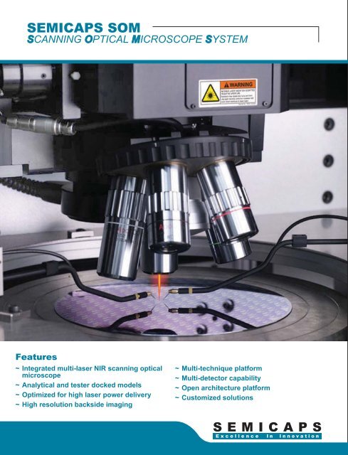
<strong>SEMICAPS</strong> <strong>SOM</strong><br />
SCANNING OPTICAL MICROSCOPE SYSTEM<br />
Features<br />
~ Integrated multi-laser NIR scanning optical<br />
microscope<br />
~ Analytical and tester docked models<br />
~ Optimized for high laser power delivery<br />
~ High resolution backside imaging<br />
~ Multi-technique platform<br />
~ Multi-detector capability<br />
~ Open architecture platform<br />
~ Customized solutions<br />
<strong>SEMICAPS</strong><br />
Excellence In Innovation
<strong>SEMICAPS</strong> <strong>SOM</strong><br />
SCANNING OPTICAL MICROSCOPE SYSTEM<br />
PRODUCT DESCRIPTION<br />
<strong>SEMICAPS</strong> <strong>SOM</strong> is a scanning optical microscope<br />
used for fault localization of integrated circuits using<br />
laser induced phenomena. It is an integrated<br />
compucentric system designed for maximum ease of<br />
use and flexibility. The system is optimized for high<br />
laser power delivery, sensitivity and spatial resolution.<br />
The open architecture of the system allows the<br />
application of current and future laser induced<br />
techniques. The modular design facilitates<br />
customization of user requirements.<br />
M u l t i - l a s e r c a p a b i l i t y<br />
The standard <strong>SEMICAPS</strong> <strong>SOM</strong><br />
system uses two near-IR lasers.<br />
The 1064nm laser is capable<br />
of efficient electron-hole pair<br />
generation through backside<br />
silicon while the 1340nm laser<br />
is a high resolution thermal<br />
probe which allows localized<br />
heating. The laser multiplexer<br />
provides seamless selection,<br />
attenuation and pulsing of the<br />
lasers. Additional lasers can<br />
also be integrated into the<br />
system.<br />
1340nm<br />
Laser<br />
Shutter<br />
Attenuation<br />
Wheel<br />
High resolution laser<br />
scan image<br />
Image resolution is up to<br />
2048x2048. The spatial<br />
resolution is less than 0.8µm for<br />
1064nm lasers using a<br />
conventional long working<br />
distance objective.<br />
<strong>SEMICAPS</strong><br />
Excellence In Innovation<br />
Fiber<br />
Focusing Lens<br />
High laser power delivery<br />
The laser power on the device is greater than 30mW<br />
for all conventional long working distance objectives.<br />
Higher spatial resolution can be achieved using the<br />
Solid Immersion Lens (SIL) option or Diffractive Lens<br />
Option.<br />
1064nm<br />
Laser<br />
Beamsplitter<br />
Multi-technique capability<br />
The system is compatible with the following thermal<br />
stimulation techniques: OBIRCH 1 , TIVA 2 , SEI, TBIP 3 ,<br />
DReM 4 , SDL-RIL 5 ; and the following carrier generation<br />
techniques: OBIC, SCOBIC 6 , LIVA 2 and LADA. The<br />
system is also upgradeable for future techniques.<br />
TV-rate camera for<br />
navigation<br />
The system incorporates a TVrate<br />
navigation camera for realtime<br />
backside imaging to<br />
complement the slow scan rate<br />
of the laser scan module.<br />
Multi-detector capability<br />
The microscope module is<br />
custom designed to provide<br />
maximum flexibility for the<br />
optical components required<br />
for various detectors and<br />
sources, e.g. Si-CCD, InGaAs,<br />
MCT, Laser Marker, etc.<br />
Two position<br />
slider. LSM<br />
or camera<br />
Two position<br />
slider<br />
High resolution stage<br />
The system comes with linear servo and linear encoder<br />
stages with 20nm resolution and repeatability better<br />
than 0.5µm. The linear servo mechanism allows the<br />
user to move the stage with minimal vibration.<br />
Proprietary laser induced signal digitization<br />
hardware<br />
The system comes with a proprietary digitization<br />
hardware capable of providing the average, sum and<br />
string of values. The summing and averaging module<br />
is capable of 1 million samples and more than 8000<br />
string values.<br />
Flexible system configurations<br />
<strong>SEMICAPS</strong> <strong>SOM</strong>s are offered in various configurations:<br />
analytical, inverted analytical, upright and inverted<br />
tester docked models.<br />
LSM<br />
Tube Lens<br />
Objectives<br />
Navigation<br />
camera<br />
Illuminator
<strong>SEMICAPS</strong> <strong>SOM</strong><br />
SCANNING OPTICAL MICROSCOPE SYSTEM<br />
APPLICATIONS<br />
Recent developments have seen the use of scanned NIR laser beams to actively localize failures which are sensitive<br />
to electron-hole pair generation or thermal stimulation. SCOBIC is an example of the electron-hole pair generation<br />
technique while OBIRCH 1 and TIVA 2 are thermal stimulation techniques used for detecting interconnect failures.<br />
SCOBIC 6 Image<br />
The single contact optical beam induced current<br />
(SCOBIC) technique overcomes the limitation of OBIC<br />
which requires contacts to both sides of the junction for<br />
imaging and characterization. SCOBIC needs only one<br />
contact, usually the substrate, to image and characterize<br />
all the junctions that are connected directly or indirectly<br />
to the contract.<br />
Gate<br />
P.Well<br />
Backside reflected image<br />
of NMOS transistor<br />
DReM<br />
image<br />
Drain<br />
Reflected image<br />
Source<br />
SD Well Junction<br />
Contact Diffusion<br />
region<br />
SD Region<br />
Backside SCOBIC image<br />
of NMOS transistor<br />
DReM 5 Image<br />
The Differential Resistance<br />
Monitor (DReM) is a patented<br />
dc coupled amplifier which<br />
provides voltage bias and<br />
voltage detection. This<br />
amplifier provides higher<br />
sensitivity and reduces the<br />
distortions in the images from<br />
conventional ac coupled<br />
amplifiers.<br />
Image<br />
from<br />
ac<br />
coupled<br />
amplifier<br />
TBIP 4 Image<br />
The patented TBIP techniques overcome the limitations<br />
of conventional laser induced techniques using TIVA 2<br />
and OBIRCH 1 by introducing an inductor to achieve<br />
voltage bias and voltage detection. Dwell time control<br />
together with pulsing and lock-in detection result in better<br />
localization accuracy and higher sensitivity.<br />
Pulsed TBIP image of a<br />
defect that cannot be<br />
detected by OBIRCH 1 or<br />
TIVA 2<br />
Overlay of reflected image<br />
with pulsed TBIP image<br />
of a defect that cannot be<br />
detected by OBIRCH 1 or<br />
TIVA 2<br />
SDL 3 Image<br />
The Soft Defect Localization (SDL) technique uses the<br />
tester as a detector of laser induced effects. At each<br />
pixel location, the tester is programmed to run the relevant<br />
portion of the test program for a specified number of<br />
cycles. The pass-fail data is then used to construct the<br />
SDL image for fault localization.<br />
SDL image Overlay of reflected image<br />
and SDL image<br />
<strong>SEMICAPS</strong><br />
Excellence In Innovation
<strong>SEMICAPS</strong> <strong>SOM</strong><br />
SCANNING OPTICAL MICROSCOPE SYSTEM<br />
<strong>SOM</strong> 1100<br />
Multi-laser<br />
Analytical <strong>SOM</strong><br />
<strong>SEMICAPS</strong> COMMITMENT<br />
<strong>SEMICAPS</strong>, an innovator and manufacturer of failure analysis equipment, is dedicated to research and development programs<br />
to bring you the latest products for integrated circuit failure analysis.<br />
All specifications are subject to change without prior notice.<br />
Note:<br />
1. OBIRCH is a patented technique by NEC<br />
2. TIVA and LIVA are patented techniques by Sandia National Laboratory<br />
3. TBIP is a set of patented techniques by Advanced Micro Devices and <strong>SEMICAPS</strong> <strong>Pte</strong> <strong>Ltd</strong><br />
4. DReM is a patented technique by <strong>SEMICAPS</strong> <strong>Pte</strong> <strong>Ltd</strong><br />
5. SDL and RIL are patented techniques by Advanced Micro Devices, Sandia National Laboratory and University of New Mexico<br />
6. SCOBIC is a patented technique by National University of Singapore<br />
<strong>SEMICAPS</strong> <strong>Pte</strong> <strong>Ltd</strong><br />
A Company of <strong>SEMICAPS</strong> Corporation Group<br />
28 Ayer Rajah Crescent #03-01<br />
Singapore 139959<br />
Tel: +65 6779-3735<br />
Fax: +65 6779-3748<br />
Email: sales@semicaps.com<br />
http://www.semicaps.com<br />
<strong>SEMICAPS</strong><br />
Excellence In Innovation<br />
<strong>SOM</strong> 3000<br />
Multi-laser Inverted<br />
Tester-docked <strong>SOM</strong><br />
DISTRIBUTOR:<br />
<strong>SOM</strong> 2000<br />
Multi-laser Upright<br />
Tester-docked <strong>SOM</strong><br />
<strong>SOM</strong> 4000<br />
Multi-laser Inverted<br />
Analytical and<br />
Tester-docked <strong>SOM</strong>