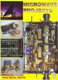
Low Noise Amplifiers For 2304 MHz Using The HP ... - transistori.net
Low Noise Amplifiers For 2304 MHz Using The HP ... - transistori.net
Low Noise Amplifiers For 2304 MHz Using The HP ... - transistori.net

You also want an ePaper? Increase the reach of your titles
YUMPU automatically turns print PDFs into web optimized ePapers that Google loves.
<strong>Low</strong> <strong>Noise</strong> <strong>Amplifiers</strong> for <strong>2304</strong>, 3456,<br />
5760, and 10368 <strong>MHz</strong> using the<br />
ATF-36077 PHEMT<br />
by<br />
Al Ward<br />
WB5LUA<br />
INTRODUCTION<br />
<strong>The</strong> Hewlett-Packard ATF-36077<br />
PHEMT device is described in a series of low<br />
noise amplifiers for <strong>2304</strong>, 3456, 5760, and<br />
10368 <strong>MHz</strong>. Single stage amplifiers are<br />
described for <strong>2304</strong>, 3456, and 5760 <strong>MHz</strong> while a<br />
two stage amplifier is described for 10368 <strong>MHz</strong>.<br />
<strong>The</strong> goal for these amplifiers was to establish a<br />
common printed circuit board size that would<br />
ultimately allow all LNAs to be built into a<br />
common aluminum waterproof enclosure.<br />
LNA DESIGN<br />
All LNAs were designed for ER=2.2<br />
dielectric material. <strong>The</strong> 10368 <strong>MHz</strong> LNA was<br />
designed for .015 inch thickness material to<br />
minimize radiation losses while the lower<br />
frequency LNAs were designed for .031 inch<br />
thickness material. I have used both Taconics<br />
TLY-5 and Rogers D5880 material with very<br />
good success. All LNAs make use of plated<br />
through holes to obtain good high frequency<br />
grounding of the PHEMT devices.<br />
All 4 LNAs use microstripline matching except<br />
for the noise match of the <strong>2304</strong> and 3456 <strong>MHz</strong><br />
LNAs where a wire inductor was used for lower<br />
loss. Quarterwave bias decoupling lines are used<br />
to provide gate and drain bias to each stage. 50 Ω<br />
resistors are used along with the bias decoupling<br />
lines to provide low frequency terminations for<br />
the devices. On the 3 low frequency units a<br />
resistor in series with the drain is used to<br />
improve stability.<br />
Each LNA will be described separately<br />
in the following sections<br />
<strong>2304</strong> <strong>MHz</strong> LNA<br />
<strong>The</strong> <strong>2304</strong> <strong>MHz</strong> LNA including<br />
component placement is shown in Figure 1. <strong>The</strong><br />
LNA uses a wire inductor for the input noise<br />
match and a microstripline match for the output<br />
with a small resistor in series with the drain to<br />
lower gain and improve stability.<br />
INPUT<br />
REDUCE TO 2.0 INCHES<br />
Vdd<br />
<strong>2304</strong>/2400 <strong>MHz</strong><br />
ATF-36077<br />
WB5LUA<br />
04/96<br />
ER=2.2<br />
Vgg H=.031<br />
OUTPUT<br />
Figure 1. <strong>2304</strong> <strong>MHz</strong> LNA showing component<br />
placement<br />
Although the ATF-36077 is capable of<br />
“device only” noise figures of nearly 0.2 dB at 2<br />
GHz, the losses of the input <strong>net</strong>work limit actual<br />
LNA noise figures to around 0.4 dB. I described<br />
another <strong>2304</strong> <strong>MHz</strong> LNA 1 that used wire
inductors for both the noise match and the input<br />
bias decoupling line. This technique allowed the<br />
LNA to achieve a noise figure of 0.4 dB or<br />
slightly less. Since this LNA was designed to be<br />
mounted in a standard enclosure I included some<br />
additional input etch which raised the noise<br />
figure slightly. <strong>The</strong> prototype LNAs I built were<br />
mounted in a box made from brass strips 1 inch<br />
tall. <strong>The</strong> SMA connectors were soldered directly<br />
to the printed circuit board and the brass walls. I<br />
was able to achieve 0.4 to 0.5 dB noise figures<br />
on all units built to date. Associated gain is 15 to<br />
16 dB typically. Bias point is Vds =2 volts and<br />
Ids = 15 mA.<br />
<strong>The</strong> schematic diagram for both the<br />
<strong>2304</strong> <strong>MHz</strong> and 3456 <strong>MHz</strong> LNAs is shown in<br />
Figure 2. <strong>The</strong> parts list is shown in Figure 3.<br />
Vgg<br />
C3<br />
INPUT<br />
C1 L1<br />
Q1 R3<br />
R1<br />
C2<br />
R2<br />
C4<br />
OUTPUT<br />
Figure 2. Schematic Diagram for <strong>2304</strong> and 3456<br />
<strong>MHz</strong> LNAs<br />
C1,C2, 8.2 to 10 pF chip capacitor<br />
C4<br />
C3,C5 1000pF // .01uF chip capacitor<br />
L1 <strong>2304</strong> <strong>MHz</strong> , length = .5 inch<br />
3456 <strong>MHz</strong>, length = .3 inch<br />
.007”diameter with .075” soldered<br />
to input etch and .025” soldered to<br />
gate lead. Adjust for best NF<br />
Q1 Hewlett-Packard ATF-36077<br />
PHEMT<br />
R1,R2 50 Ω chip resistor<br />
R3 10 to 27 Ω chip resistor (effects<br />
gain and stability)<br />
R4 <strong>For</strong> operation from a power supply<br />
voltage of 5 volts, R4 = 200Ω - R3<br />
- R2<br />
Figure 3. Parts list for <strong>2304</strong> and 3456 <strong>MHz</strong><br />
LNAs<br />
3456 <strong>MHz</strong> LNA<br />
C5<br />
R4<br />
Vdd<br />
<strong>The</strong> 3456 <strong>MHz</strong> LNA including<br />
component placement is shown in Figure 4. <strong>The</strong><br />
LNA design is very similar to the <strong>2304</strong> <strong>MHz</strong><br />
LNA. It also uses a wire inductor for the input<br />
noise match and a microstripline match for the<br />
output <strong>net</strong>work. A small resistor in series with<br />
the drain is used to lower gain and improve<br />
stability.<br />
INPUT<br />
Vdd<br />
REDUCE TO 2.0 INCHES<br />
ATF-36077<br />
3456 <strong>MHz</strong><br />
Vgg<br />
WB5LUA<br />
04/96<br />
ER=2.2<br />
H=.031<br />
OUTPUT<br />
Figure 4. 3456 <strong>MHz</strong> LNA showing component<br />
layout<br />
<strong>The</strong> prototype 3456 <strong>MHz</strong> LNAs were<br />
installed in brass housings similar to the <strong>2304</strong><br />
<strong>MHz</strong> LNA. <strong>Noise</strong> figures of 0.6 to 0.7 dB were<br />
obtained along with 13 to 14 dB gain. <strong>The</strong><br />
resistor in series with the drain can be lowered in<br />
value to increase gain and lower noise figure<br />
slightly. Somewhat lower noise figure could<br />
possibly be obtained by cutting off the input 50<br />
Ω microstripline and placing the input connector<br />
adjacent to the input blocking capacitor. Bias<br />
point is Vds =2 volts and Ids = 15 mA.<br />
5760 <strong>MHz</strong> LNA<br />
<strong>The</strong> 5760 <strong>MHz</strong> LNA including<br />
component placement is shown in Figure 5. <strong>The</strong><br />
LNA uses microstripline matching <strong>net</strong>works for<br />
both the input noise match and output gain<br />
match. Some resistive loading in the drain circuit<br />
is required for unconditional stability, according<br />
to the computer analysis. However, several<br />
LNAs have been built without this resistor with<br />
no problems experienced.
<strong>The</strong> prototype 5760 <strong>MHz</strong> LNAs were<br />
installed in brass housings similar to the other<br />
LNAs. <strong>Noise</strong> figures of 0.7 to 0.8 dB were<br />
obtained along with 12 to 13 dB gain. Somewhat<br />
lower noise figure could possibly be obtained by<br />
cutting off the input 50 Ω microstripline and<br />
placing the input connector adjacent to the input<br />
blocking capacitor. Bias point is Vds =2 volts<br />
and Ids = 15 mA.<br />
<strong>The</strong> schematic diagram and parts list are<br />
shown in Figures 6 and 7.<br />
Vgg<br />
C3<br />
INPUT C1 Q1<br />
R1<br />
R3<br />
R2<br />
C4<br />
C5<br />
OUTPUT<br />
Figure 6 Schematic Diagram of 5760 <strong>MHz</strong> LNA<br />
C2<br />
R4<br />
Vdd<br />
C1,C2, 1 pF chip capacitor (1-2 pF OK)<br />
C4 10 pF chip capacitor<br />
C3,C5 1000pF // .01uF chip capacitor<br />
Q1 Hewlett-Packard ATF-36077<br />
PHEMT<br />
R1,R2 50 Ω chip resistor<br />
R3 10 to 27 Ω chip resistor (effects<br />
gain and stability)<br />
R4 <strong>For</strong> operation from a power supply<br />
voltage of 5 volts, R4 = 200Ω - R3<br />
- R2<br />
Figure 7. Parts list for 5760 <strong>MHz</strong> LNA<br />
10368 <strong>MHz</strong> LNA<br />
<strong>The</strong> 10368 <strong>MHz</strong> LNA was designed as<br />
a 2 stage LNA in an attempt to lower “low<br />
frequency” gain which became a problem when<br />
mating an earlier design single stage unit with a<br />
waveguide input configuration. With a single<br />
stage LNA, gain peaking in the 7 GHz frequency<br />
range coupled with the rolloff of the high pass<br />
nature of WR-90 produced some instabilities.<br />
<strong>The</strong> 2 stage 10368 <strong>MHz</strong> LNA is shown<br />
in Figure 8. <strong>The</strong> LNA uses microstripline<br />
matching throughout the amplifier. <strong>The</strong> input<br />
<strong>net</strong>work provides the noise match. Both the<br />
output matching <strong>net</strong>work and the interstage<br />
INPUT<br />
REDUCE TO 2.0 INCHES<br />
Vdd<br />
ATF-36077<br />
Vgg<br />
5760 <strong>MHz</strong><br />
WB5LUA<br />
03/96<br />
ER=2.2<br />
T=.031<br />
OUTPUT<br />
Figure 5. 5760 <strong>MHz</strong> LNA showing component placement<br />
CUT OFF STUB<br />
matching <strong>net</strong>work were design for reasonable<br />
gain at 10368 <strong>MHz</strong> while providing some low<br />
frequency rolloff.<br />
IN<br />
ADD STUBS, SEE NOTE 4<br />
REDUCE TO 2.0 INCHES<br />
Vdd<br />
Rd2<br />
Rd1<br />
WB5LUA 10368 <strong>MHz</strong><br />
04/96<br />
ATF-36077 ATF-36077<br />
Vgg1<br />
ER=2.2<br />
T=.015<br />
Vgg2<br />
OUT<br />
Figure 8. 10368 <strong>MHz</strong> LNA showing component<br />
placement<br />
<strong>The</strong> prototype 10368 <strong>MHz</strong> LNAs were<br />
installed in brass housings. I used .75 inch wide<br />
brass for the 4 walls. With the higher gain of the<br />
2 stage amplifier, the effect of the housing<br />
became more noticeable especially when<br />
attaching a cover to the box. I made use of a .5<br />
inch wide piece of brass as a divider down the<br />
middle of the amplifier. This is shown in Figure<br />
8. <strong>The</strong> .5 inch wide piece of brass is placed .85<br />
inch in from the side of the box. This makes it<br />
slightly offset from being run directly down the<br />
middle of the box. <strong>The</strong> divider is soldered to the<br />
walls of the box in such a way that it will make<br />
contact with the cover and be about .2 inch above<br />
the printed circuit board etch. This divider tends<br />
to break up the waveguide effect of the<br />
enclosure which tends to help propagation of<br />
unwanted waves through the box., causing<br />
undesired feedback. I also made use of some<br />
absorber material as shown in Figure 8.<br />
0.5 INCH HIGH BRASS DIVIDER<br />
ABSORBER MATERIAL ON INSIDE WALL
Some tuning of the initial design was<br />
necessary. I used .04 by .1 inch stubs cut from<br />
some transistor leads. Place 1 stub as shown on<br />
the input line. See Figure 8. This may necessitate<br />
some tuning depending on the type and quality of<br />
the SMA connectors you have in your junk box.<br />
Use 2 more stubs to widen the output etch as<br />
shown on Q1.<br />
<strong>Noise</strong> figures of 0.7 to 1.0 dB were<br />
obtained along with 23 dB gain. Bias point is<br />
Vds =1.5 volts and Ids = 15 mA per device.<br />
<strong>The</strong> schematic diagram and parts list are shown<br />
in Figures 9 and 10..<br />
INPUT<br />
Vgg1<br />
C4<br />
Add<br />
C1<br />
R1<br />
Vdd1<br />
C5<br />
Q1<br />
R2<br />
Add<br />
C2<br />
R3<br />
Vdd2<br />
Q2<br />
C7<br />
Vgg2<br />
C6<br />
Figure 9. Schematic Diagram of 2 stage 10368<br />
<strong>MHz</strong> LNA<br />
C1 0.6 pF chip capacitor (0.5-1 pF OK)<br />
C2,C3 1 pF chip capacitor (1-2pF OK)<br />
C4,C5, 1000pF // .01uF chip capacitor<br />
C6,C7<br />
Q1,Q2 Hewlett-Packard ATF-36077<br />
PHEMT<br />
R1,R2, 50 Ω chip resistor<br />
R3,R4<br />
RD1 <strong>For</strong> operation from a power supply<br />
RD2 voltage of 5 volts, RD1=RD2 =<br />
180Ω<br />
Figure 10. Parts list for 10368 <strong>MHz</strong> LNA<br />
Biasing<br />
I use passive biasing in most of my<br />
amplifiers with good success. I use a regulated 5<br />
volt source which also feeds the dc-dc converter<br />
which generates the negative voltage .. I use a<br />
potentiometer off the negative source to set the<br />
proper gate voltage required to sustain 10 to 15<br />
mA drain current. <strong>The</strong> resistance between the 5<br />
volt power supply and the drain of the device is<br />
calculated based on a 3 volt drop to the drain.<br />
<strong>The</strong> actual dc bias point of the device is not that<br />
critical. Vds can be anything from 1.5 to 2 volts<br />
and drain current can be between 10 and 15 mA.<br />
DC to DC converters and various passive and<br />
R4<br />
C3<br />
OUTPUT<br />
active bias schemes are covered in other<br />
articles. 23 .<br />
Downeast Microwave offers both single<br />
and dual stage power supplies for powering up<br />
FETs. (Part numbers PPS-1 and PPS-2) A<br />
potentiometer is used to set the gate voltage. <strong>The</strong><br />
important thing to remember is to set the gate<br />
voltage at about -0.2 v before applying the drain<br />
voltage or before installing the bias resistors on<br />
the board. <strong>The</strong> worst thing you can do to a fet is<br />
to apply a high enough negative voltage to the<br />
gate that it “pinches off the drain” and causes no<br />
current to flow. With several volts negative on<br />
the gate and 5 volts positive on the drain, the<br />
device is history, even before it even thought<br />
about operating!. It is best to pre-set the gate<br />
voltage to where there is some drain current<br />
being pulled through the drain bias resistors. <strong>The</strong><br />
gate voltage can then be set for optimum drain<br />
current which should coincide with maximum<br />
gain and nearly minimum noise figure. A good<br />
test for an LNA is to determine if optimum gain<br />
and noise performance occur coincidentally<br />
within the range of the specified bias point. If the<br />
LNA is oscillating, then as one increases drain<br />
current and drain voltage, the amplifier<br />
performance, i.e. gain, will peak at a much lower<br />
bias point. This signifies that the device is<br />
oscillating and going into a self-bias mode<br />
because of oscillations.<br />
Enclosures<br />
My preferred choice for an enclosure is<br />
normally a box made from brass strips.. This<br />
allows gold plated SMA connectors and the<br />
printed circuit board to be soldered directly to<br />
the brass. This provides a good RF tight box.<br />
Unfortunately when the box surrounds the circuit<br />
board, it begins to look like a piece of waveguide<br />
when viewed from either the input or output<br />
connector. <strong>The</strong> best solution would be to design<br />
the circuit board to be very narrow as viewed<br />
from the end. This will tend to look like a piece<br />
of higher frequency waveguide and will tend to<br />
rolloff lower frequencies and consequently<br />
attenuate signals that are propagating through the<br />
box and not the circuit.<br />
Solutions to the ‘waveguide effect”<br />
problem include the use of dividers to break up<br />
this phenomena. I described this technique in the<br />
section on the 10368 <strong>MHz</strong> amplifier. I have also<br />
used this same technique for the lower frequency<br />
amplifiers on occasion. If you come across an<br />
amplifier that does not seem to like having a
cover placed on it, then try this divider on top of<br />
or slightly offset from the centerline of the<br />
circuit. <strong>The</strong> top of the divider should hit the lid<br />
and the bottom should be about .2 inches above<br />
the microstrip. <strong>The</strong> divider is parallel to the side<br />
walls. Be careful not to drop it on the circuit<br />
when finding the sweet spot.<br />
Another solution is the use of absorber<br />
along at least one of the side walls. This tends to<br />
minimize unwanted reflections off the side walls<br />
which are the primary source of trouble. It was<br />
brought to my attention by Bill Janssen,<br />
K7NOM, back in 1995 that suitable microwave<br />
absorber can be found locally. In fact, Bill says<br />
there is a large supply of this stuff alongside most<br />
highways in the form of old rubber from truck<br />
tires. Sure enough, it does have some microwave<br />
absorption properties!. So if you get desperate,<br />
check the highways, but be careful! Bill<br />
attributes the absorbing properties to the carbon<br />
added to improve the ultra-violet resistance.<br />
An alternative to the brass box approach<br />
is the aluminum housing approach that I<br />
mentioned earlier. I designed the amplifiers to fit<br />
inside an aluminum housing that is available<br />
from Downeast Microwave, part number “Rose-<br />
S”. Steve makes a special pallet out of .25 inch<br />
thickness aluminum that spans the distance<br />
between the input and output connectors. It<br />
makes a tight fit in the enclosure and the SMA<br />
connectors thread into the edge of the inner<br />
pallet. <strong>The</strong> circuit board is then installed onto the<br />
aluminum pallet. I use small 4-40 hardware to<br />
hold the board down to the pallet<br />
I have also found that the liberal use of<br />
conductive epoxy insures that the ground plane<br />
of the printed circuit board makes good RF<br />
connection along the entire surface of the<br />
aluminum pallet. I have used “Circuit Works<br />
Conductive Epoxy” part number 2400 with good<br />
success. It is a 2 part mix and once the tubes<br />
have been opened once, it appears that shelf life<br />
is not very long, so it is best to do several<br />
amplifiers at one time. Steve at Downeast<br />
Microwave uses shim stock to help enhance the<br />
RF connection between the pallet, circuit board,<br />
and the inside surface of the enclosure which<br />
then mates with the RF connectors.<br />
Based on several amplifiers built to date<br />
it appears that the noise figure of the units built<br />
in the aluminum housings are within a 0.1 dB of<br />
the brass box units. I have also noticed that none<br />
of the aluminum housing units seem to have any<br />
stability issues when installing the covers. This<br />
could be due to the fact that the sides of the<br />
aluminum pallet and therefore the sides of the<br />
printed circuit board are suspended in the<br />
housing. As I mentioned before, it is the side<br />
walls of the amplifier that give rise to the<br />
“waveguide effect” problem. With the aluminum<br />
housing units, there is a gap or discontinuity<br />
between the side edge of the board and the inside<br />
edge of the housing.<br />
Closing<br />
Hopefully, these LNAs will provide a<br />
boost to both your terrestrial and moonbounce<br />
systems as they have to mine.<br />
A.J.Ward<br />
09-09-97<br />
References<br />
1. A.J.Ward, “<strong>Low</strong> <strong>Noise</strong> Amplifier for <strong>2304</strong><br />
<strong>MHz</strong> using the <strong>HP</strong> ATF-36077 PHEMT<br />
Device”, Proceedings of Microwave Update ‘94,<br />
pg.8-10<br />
2. A.J. Ward, “Simple <strong>Low</strong> <strong>Noise</strong> Preamplifiers”,<br />
QST, May, 1989, pg 31-36<br />
3. <strong>Using</strong> the ATF-10236 in <strong>Low</strong> <strong>Noise</strong> Amplifier<br />
Applications in the UHF through 1.7 GHz<br />
Frequency Range, Hewlett Packard Application<br />
Note 1076, publication number 5963-<br />
3780E(3/95)