

Michel Waleczek
Michel Waleczek
Michel Waleczek

Create successful ePaper yourself
Turn your PDF publications into a flip-book with our unique Google optimized e-Paper software.
called a depletion type, is scarcely<br />
used any more.<br />
Measuring FET<br />
parameters<br />
Field-effect transistors (FETs) can be<br />
characterised by a certain number of<br />
parameters, but here we are only inter-<br />
36<br />
12mA5<br />
ID<br />
100k<br />
R G<br />
G<br />
VGS1<br />
A<br />
+5V +5V<br />
230 Ω<br />
D<br />
S<br />
65Ω<br />
135 Ω<br />
R D<br />
JFET N JFET N<br />
VGS2 S<br />
R SW<br />
ID1<br />
R S<br />
VDS<br />
biasing of circuit<br />
VDS1<br />
bias in linear zone<br />
VGS = 0V6<br />
A<br />
5V<br />
12mA5<br />
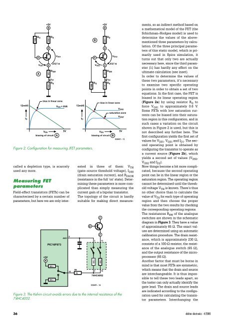
Figure 2. Configuration for measuring JFET parameters.<br />
+5V<br />
PIC16F873<br />
65Ω<br />
25Ω<br />
AN3<br />
5<br />
ID<br />
100k<br />
B<br />
G<br />
R G<br />
230 Ω<br />
D<br />
65Ω<br />
135 Ω<br />
R D<br />
R SW<br />
R S<br />
VDS2<br />
ested in three of them: V TH<br />
(gate–source threshold voltage), I DSS<br />
(drain saturation current), and R DSON<br />
(resistance in the full ‘on’ state). Determining<br />
these parameters is more complicated<br />
than simply measuring the<br />
current gain of a bipolar transistor.<br />
The topology of the circuit is hardly<br />
suitable for making direct measure-<br />
B<br />
ID2<br />
bias in linear zone<br />
VDS<br />
biasing of circuit<br />
65Ω<br />
65Ω<br />
16<br />
R9<br />
1k<br />
2 15<br />
74HC4052<br />
3<br />
C<br />
E<br />
030451 - 14<br />
13<br />
VGS2<br />
saturation zone<br />
VGS2'<br />
B<br />
5V<br />
030451 - 13<br />
Figure 3. The Kelvin circuit avoids errors due to the internal resistance of the<br />
74HC4052.<br />
ments, so an indirect method based on<br />
a mathematical model of the FET (the<br />
Schichman–Hodges model) is used to<br />
determine the values of the abovementioned<br />
three parameters by calculation.<br />
Of the three principal parameters<br />
of this static model, which is primarily<br />
used in Spice simulation, it<br />
turns out that only two are actually<br />
necessary here, since the third parameter<br />
(λ) has hardly any effect on the<br />
ultimate calculation (see inset).<br />
In order to determine the values of<br />
these two parameters, it’s necessary<br />
to examine two specific operating<br />
points in order to obtain a set of two<br />
equations. In the first case, the FET is<br />
biased in its linear operating region<br />
(Figure 2a) by using resistor R G to<br />
force V GS1 to approximately 0.6 V.<br />
Some FETs with low saturation currents<br />
can be biased into their saturation<br />
region in this configuration, and in<br />
such cases a variation on the circuit<br />
shown in Figure 2 is used, but this is<br />
not described any further here. The<br />
first configuration yields the first set of<br />
values for V DS1 , V GS1 and I D1 . The second<br />
operating point is obtained by<br />
configuring the transistor to operate as<br />
a current source (Figure 2b), which<br />
yields a second set of values (V DS2 ,<br />
V GS2 and I D2 ).<br />
Now things become a bit more complicated,<br />
because the second operating<br />
point can lie in the linear region or the<br />
saturation region. The operating region<br />
cannot be determined until the threshold<br />
voltage V TH is known. There’s thus<br />
no other choice than to calculate the<br />
value of V TH for each type of operating<br />
region and then choose the proper<br />
value from the two results by checking<br />
the corresponding operating regions.<br />
The resistances R SW of the analogue<br />
switches are shown in the schematic<br />
diagram in Figure 3. They have a value<br />
of approximately 65 Ω. The exact values<br />
are determined using an automatic<br />
calibration procedure. The drain resistance,<br />
which is approximately 230 Ω,<br />
consists of a 100-Ω resistor, the resistance<br />
of the analogue switch (65 Ω),<br />
and the output resistance of the microprocessor<br />
(65 Ω).<br />
Another factor that must be borne in<br />
mind is that most FETs are symmetric,<br />
which means that the drain and source<br />
are interchangeable. It is thus impossible<br />
to tell these two leads apart, so<br />
the tester can only actually identify the<br />
gate lead. The drain and source leads<br />
are indicated according to the configuration<br />
used for calculating the transistor<br />
parameters. Interchanging the<br />
elektor electronics - 4/2005