LF198/LF298/LF398, LF198A/LF398A Monolithic Sample-and-Hold ...
LF198/LF298/LF398, LF198A/LF398A Monolithic Sample-and-Hold ...
LF198/LF298/LF398, LF198A/LF398A Monolithic Sample-and-Hold ...

Create successful ePaper yourself
Turn your PDF publications into a flip-book with our unique Google optimized e-Paper software.
Application Hints (Continued)<br />
logic input for signal delay, calculate the slope of the waveform<br />
at the threshold point to ensure that it is at least<br />
1.0 V/µs.<br />
Sampling Dynamic Signals<br />
<strong>Sample</strong> error to moving input signals probably causes more<br />
confusion among sample-<strong>and</strong>-hold users than any other parameter.<br />
The primary reason for this is that many users make<br />
the assumption that the sample <strong>and</strong> hold amplifier is truly<br />
locked on to the input signal while in the sample mode. In actuality,<br />
there are finite phase delays through the circuit creating<br />
an input-output differential for fast moving signals. In addition,<br />
although the output may have settled, the hold<br />
capacitor has an additional lag due to the 300Ω series resistor<br />
on the chip. This means that at the moment the “hold”<br />
comm<strong>and</strong> arrives, the hold capacitor voltage may be somewhat<br />
different than the actual analog input. The effect of<br />
these delays is opposite to the effect created by delays in the<br />
logic which switches the circuit from sample to hold. For example,<br />
consider an analog input of 20 Vp-p at 10 kHz. Maximum<br />
dV/dt is 0.6 V/µs. With no analog phase delay <strong>and</strong> 100<br />
ns logic delay, one could expect up to (0.1 µs) (0.6V/µs)<br />
= 60 mVerror if the “hold” signal arrived near maximum dV/dt<br />
of the input. A positive-going input would give a +60 mV error.<br />
Now assume a 1 MHz (3 dB) b<strong>and</strong>width for the overall<br />
analog loop. This generates a phase delay of 160 ns. If the<br />
hold capacitor sees this exact delay, then error due to analog<br />
delay will be (0.16 µs) (0.6 V/µs) = −96 mV. Total output error<br />
is +60 mV (digital) −96 mV (analog) for a total of −36 mV. To<br />
add to the confusion, analog delay is proportioned to hold<br />
capacitor value while digital delay remains constant. A family<br />
of curves (dynamic sampling error) is included to help estimate<br />
errors.<br />
A curve labeled Aperture Time has been included for sampling<br />
conditions where the input is steady during the sampling<br />
period, but may experience a sudden change nearly<br />
coincident with the “hold” comm<strong>and</strong>. This curve is based on<br />
a 1 mV error fed into the output.<br />
A second curve, <strong>Hold</strong> Settling Time indicates the time required<br />
for the output to settle to 1 mV after the “hold” comm<strong>and</strong>.<br />
Digital Feedthrough<br />
Fast rise time logic signals can cause hold errors by feeding<br />
externally into the analog input at the same time the amplifier<br />
is put into the hold mode. To minimize this problem, board<br />
layout should keep logic lines as far as possible from the<br />
analog input <strong>and</strong> the Ch pin. Grounded guarding traces may<br />
also be used around the input line, especially if it is driven<br />
from a high impedance source. Reducing high amplitude<br />
logic signals to 2.5V will also help.<br />
7<br />
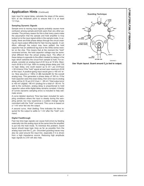
Guarding Technique<br />
DS005692-5<br />
Use 10-pin layout. Guard around C his tied to output.<br />
www.national.com<br />
<strong>LF198</strong>/<strong>LF298</strong>/<strong>LF398</strong>, <strong>LF198</strong>A/<strong>LF398</strong>A