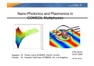
Presentation - Computational Optics Group
Presentation - Computational Optics Group
Presentation - Computational Optics Group

You also want an ePaper? Increase the reach of your titles
YUMPU automatically turns print PDFs into web optimized ePapers that Google loves.
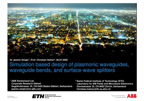
Dr Jasmin Smajic<br />
Simulation based design of plasmonic waveguides,<br />
waveguide bends, and surface-wave splitters<br />
1 , Prof. Christian Hafner2 , 06.07.2009<br />
1 ABB Switzerland Ltd.<br />
Corporate Research Dättwil<br />
Segelhofstrasse 1K, CH-5405 Baden-Dättwil, Switzerland<br />
jasmin.smajic@ch.abb.com<br />
© ABB <strong>Group</strong><br />
July 8, 2009 | Slide 1<br />
2 Swiss Federal Institute of Technology (ETH)<br />
Laboratory for EM Fields and Microwave Electronics<br />
Gloriastrasse 35, CH-8092 Zürich, Switzerland<br />
Christian.hafner@ifh.ee.ethz.ch
Outline<br />
© ABB <strong>Group</strong><br />
July 8, 2009 | Slide 2<br />
Introduction<br />
Plasmon resonance<br />
Surface plasmon polaritons<br />
Numerical methods for analysis of the plasmonic<br />
structures<br />
Waveguide structures<br />
Plasmonic slotline waveguide (PSWG)<br />
Metalic heterowaveguide (MHWG)<br />
2D eigenvalue analysis<br />
3D analysis of the waveguide<br />
Waveguide bend<br />
3D analysis of the 90º waveguide bend<br />
Plasmonic surface wave splitter<br />
2D analysis of the surface wave splitter<br />
Outlook
Introduction<br />
Plasmon Resonance<br />
Plasmon effect: the effect of collective vibrations of electrons in metal at<br />
infrared and optical frequencies<br />
Surface plasmon: the fluctuations of electron density at the metal-insulator<br />
interface<br />
Surface plasmon polariton: a surface plasmon coupled with photon<br />
The excited polariton propagates over the metal’s outer surface until it is<br />
either converted back into a photon or absorbed by the crystal lattice as a<br />
phonon<br />
Surface plasmon resonance (SPR): the excitation of the surface plasmons by<br />
external EM radiation<br />
Localized surface plasmon resonance (LSPR): metalic structure smaller than<br />
the wavelength<br />
Metal at optical and infrared frequencies: described as a homogenous<br />
domain with complex dielectric permittivity<br />
© ABB <strong>Group</strong><br />
July 8, 2009 | Slide 3
Introduction<br />
Surface Plasmon Polaritons<br />
© ABB <strong>Group</strong><br />
July 8, 2009 | Slide 4<br />
omega (1/s)<br />
x 1015<br />
12<br />
10<br />
8<br />
6<br />
4<br />
2<br />
air<br />
silica<br />
surface plasmon<br />
0 0.5 1 1.5 2 2.5 3 3.5 4 4.5 5<br />
x 10 7<br />
0<br />
beta (1/m)
Introduction<br />
Surface Plasmon Polaritons<br />
© ABB <strong>Group</strong><br />
July 8, 2009 | Slide 5<br />
Propagation length (um)<br />
1000<br />
900<br />
800<br />
700<br />
600<br />
500<br />
400<br />
300<br />
200<br />
100<br />
0<br />
0 500 1000 1500 2000 2500<br />
wavelength (nm)
Introduction<br />
Surface Plasmon Polaritons<br />
Propagation length (um)<br />
1000<br />
900<br />
800<br />
700<br />
600<br />
500<br />
400<br />
300<br />
200<br />
100<br />
© ABB <strong>Group</strong><br />
July 8, 2009 | Slide 6<br />
|Ey | 0.2 m<br />
2 |Ey | 2<br />
350nm<br />
0<br />
0 500 1000 1500 2000 2500<br />
wavelength (nm)<br />
|E y | 2<br />
370nm<br />
Propagation length (um)<br />
360nm<br />
20<br />
15<br />
10<br />
5<br />
0<br />
0.2 m<br />
200 250 300 350 400 450 500<br />
wavelength (nm)<br />
0.2 m
Introduction<br />
Numerical Methods<br />
© ABB <strong>Group</strong><br />
July 8, 2009 | Slide 7<br />
Domain Methods Boundary Methods<br />
Finite Element Method (FEM)<br />
Finite Difference<br />
Time Domain (FDTD)<br />
Multiple Multipole<br />
Program (MMP)<br />
Method of Auxiliary<br />
Sources (MAS)<br />
Meshless Boundary Integral<br />
Equation (BIE) Approach<br />
J. Smajic et al., “Comparison of Numerical Methods for the Analysis of<br />
Plasmonic Structures”, Journal of <strong>Computational</strong> and Theoretical<br />
Nanoscience, Vol. 6, No. 3, pp. 763-774, 2009.
Waveguide Structures<br />
Plasmonic slotline waveguide (PSWG)<br />
Description<br />
Geometry<br />
and materials<br />
© ABB <strong>Group</strong><br />
July 8, 2009 | Slide 8<br />
A plasmonic slotline is an air slot in a thin silver film deposited on a<br />
silica substrate.<br />
The dimensions of the slot are much smaller than the wavelength.<br />
The goal is to find a bound optical mode supported by the slotline.<br />
50nm<br />
Silver<br />
50nm<br />
Silica<br />
Silver<br />
G. Veronis et al., “Guided subwavelength plasmonic mode supported by a<br />
slot in a thin metal film”, <strong>Optics</strong> Letters, Vol. 30, pp. 3359-3361, 2005.
Plasmonic Slotline<br />
2D Eigenvalue Analysis<br />
Analysis<br />
Modeling<br />
© ABB <strong>Group</strong><br />
July 8, 2009 | Slide 9<br />
Assumption: The bound mode is a hybrid mode.<br />
Analysis: 2D vector elements are required.<br />
Open boundary: PML absorbing boundary conditions are needed.<br />
PML
Plasmonic Slotline<br />
2D Eigenvalue Analysis<br />
Analysis<br />
Modeling<br />
© ABB <strong>Group</strong><br />
July 8, 2009 | Slide 10<br />
Bound mode: E x and Hy dominant (quasy-TEM, easy to excite by<br />
linearly polarized light).<br />
Significant propagation losses in silver<br />
The z-component of time-average<br />
Poynting vector is shown at 750nm.
Plasmonic Slotline<br />
2D Eigenvalue Analysis<br />
Results<br />
© ABB <strong>Group</strong><br />
July 8, 2009 | Slide 11<br />
0.12<br />
0.11<br />
0.1<br />
0.09<br />
0.08<br />
0.07<br />
0.06<br />
0.05<br />
0.04<br />
bound mode<br />
light line (air)<br />
light line (silica)<br />
0.03<br />
0 0.05 0.1 0.15 0.2 0.25 0.3 0.35<br />
Dispersion relation of the fundamental mode<br />
of the slotline (red) is shown.
Plasmonic Slotline<br />
2D Eigenvalue Analysis<br />
Results<br />
© ABB <strong>Group</strong><br />
July 8, 2009 | Slide 12<br />
Lpr (um)<br />
14<br />
12<br />
10<br />
8<br />
6<br />
4<br />
2<br />
0<br />
0.4 0.6 0.8 1 1.2 1.4 1.6 1.8<br />
wavelength (um)<br />
Propagation length of the fundamental<br />
mode of the slotline is shown.
Plasmonic Slotline<br />
2D Eigenvalue Analysis<br />
Results<br />
© ABB <strong>Group</strong><br />
July 8, 2009 | Slide 13<br />
0.12<br />
0.1<br />
0.08<br />
0.06<br />
0.04<br />
0.02<br />
w=50nm<br />
w=25nm<br />
0<br />
0 0.05 0.1 0.15 0.2 0.25 0.3 0.35<br />
Dispersion relation of the fundamental mode<br />
of the slotline (dark blue) is shown.
Plasmonic Slotline<br />
2D Eigenvalue Analysis<br />
Results<br />
© ABB <strong>Group</strong><br />
July 8, 2009 | Slide 14<br />
Lpr (um)<br />
14<br />
12<br />
10<br />
8<br />
6<br />
4<br />
2<br />
w=50nm<br />
w=25nm<br />
0<br />
0.4 0.6 0.8 1 1.2 1.4 1.6 1.8<br />
wavelength (um)<br />
Propagation length of the fundamental<br />
mode of the slotline is shown.
Waveguide Structures<br />
Metalic Heterowaveguide (MHWG)<br />
Description<br />
Geometry<br />
and materials<br />
© ABB <strong>Group</strong><br />
July 8, 2009 | Slide 15<br />
The dimensions of the structure are smaller than the wavelength.<br />
The goal is to find a bound optical mode supported by the MHWG.<br />
L. Chen et al., “High efficiency 90ºbending metal heterowaveguides for<br />
nanophotonic integration”, Applied Physics Letters, Vol. 89, pp. 243120, 2006.
Waveguide Structures<br />
Metalic Heterowaveguide (MHWG)<br />
Analysis<br />
Modeling<br />
© ABB <strong>Group</strong><br />
July 8, 2009 | Slide 16<br />
Bound mode: E x and Hy dominant (quasy-TEM, easy to excite by<br />
linearly polarized light).<br />
Significant propagation losses in metals<br />
The z-component of time-average<br />
Poynting vector is shown at 750nm.
Waveguide Structures<br />
Metalic Heterowaveguide (MHWG)<br />
Results<br />
© ABB <strong>Group</strong><br />
July 8, 2009 | Slide 17<br />
0.12<br />
0.11<br />
0.1<br />
0.09<br />
0.08<br />
0.07<br />
0.06<br />
0.05<br />
0.04<br />
bound mode MHWG<br />
bound mode PSWG<br />
light line (air)<br />
light line (silica)<br />
0.03<br />
0 0.05 0.1 0.15 0.2 0.25 0.3 0.35<br />
Dispersion relation of the fundamental mode<br />
of the MHWG and PSWG is shown.
Waveguide Structures<br />
Metalic Heterowaveguide (MHWG)<br />
Results<br />
© ABB <strong>Group</strong><br />
July 8, 2009 | Slide 18<br />
Lpr (um)<br />
15<br />
10<br />
5<br />
bound mode MHWG<br />
bound mode PSWG<br />
0<br />
0.4 0.6 0.8 1 1.2 1.4 1.6 1.8<br />
wavelength (um)<br />
Propagation length of the fundamental<br />
mode of the MHWG and PSWG is shown.
Waveguide Structures<br />
3D Waveguide<br />
© ABB <strong>Group</strong><br />
July 8, 2009 | Slide 19<br />
Silver is modeled as a<br />
homogenous material with<br />
complex permittivity<br />
50nm<br />
50nm<br />
Silica substrate, n=1.44
Waveguide Structures<br />
3D Waveguide<br />
© ABB <strong>Group</strong><br />
July 8, 2009 | Slide 20<br />
Losses in silver (3D) = 34.43%<br />
Losses in silver (2D) = 32.77%<br />
100%<br />
61.3%<br />
Time-average Poynting vector<br />
of the fundamental mode of the slotline is shown.
Waveguide Structures<br />
3D Waveguide<br />
© ABB <strong>Group</strong><br />
July 8, 2009 | Slide 21<br />
The electric field confinement of the fundamental<br />
mode of the slotline is presented.
Waveguide Bend<br />
3D analysis of the 90ºwaveguide bend<br />
© ABB <strong>Group</strong><br />
July 8, 2009 | Slide 22
Waveguide Bend<br />
3D analysis of the 90ºwaveguide bend<br />
© ABB <strong>Group</strong><br />
July 8, 2009 | Slide 23<br />
Losses in silver (3D) = 42.98%<br />
Losses in silver (2D) = 42.30%<br />
100%<br />
23.9%<br />
Time-average Poynting vector<br />
of the fundamental mode of the slotline is shown.
Plasmonic Surface Wave Splitter<br />
2D Analysis of the Surface Wave Splitter<br />
Geometry<br />
Modeling<br />
© ABB <strong>Group</strong><br />
July 8, 2009 | Slide 24
Plasmonic Surface Wave Splitter<br />
2D Analysis of the Surface Wave Splitter<br />
© ABB <strong>Group</strong><br />
July 8, 2009 | Slide 25
Outlook<br />
© ABB <strong>Group</strong><br />
July 8, 2009 | Slide 26<br />
Modern 3D simulation models are very close to reality<br />
and therefore make virtual prototyping and design<br />
optimization possible<br />
High level of spatial discretization required for<br />
accurate analysis of the plasmonic structures can be<br />
achieved today even in the case of complicated 3D<br />
structures<br />
Presented waveguide solutions (PSWG) are within the<br />
current fabrication abilities<br />
Problem of losses in metal is an important drawback
© ABB <strong>Group</strong><br />
July 8, 2009 | Slide 27