

1-Kb, 2-Kb, 4-Kb, 8-Kb and 16-Kb CMOS Serial EEPROM
1-Kb, 2-Kb, 4-Kb, 8-Kb and 16-Kb CMOS Serial EEPROM
1-Kb, 2-Kb, 4-Kb, 8-Kb and 16-Kb CMOS Serial EEPROM

You also want an ePaper? Increase the reach of your titles
YUMPU automatically turns print PDFs into web optimized ePapers that Google loves.
CAT24C01/02/04/08/<strong>16</strong><br />
1-<strong>Kb</strong>, 2-<strong>Kb</strong>, 4-<strong>Kb</strong>, 8-<strong>Kb</strong> <strong>and</strong> <strong>16</strong>-<strong>Kb</strong> <strong>CMOS</strong> <strong>Serial</strong> <strong>EEPROM</strong><br />
FEATURES<br />
■ Supports St<strong>and</strong>ard <strong>and</strong> Fast I 2 C Protocol<br />
■ 1.8 V to 5.5 V Supply Voltage Range<br />
■ <strong>16</strong>-Byte Page Write Buffer<br />
■ Hardware Write Protection for entire memory<br />
■ Schmitt Triggers <strong>and</strong> Noise Suppression Filters<br />
on I 2 C Bus Inputs (SCL <strong>and</strong> SDA).<br />
■ Low power <strong>CMOS</strong> technology<br />
■ 1,000,000 program/erase cycles<br />
■ 100 year data retention<br />
■ Industrial <strong>and</strong> Extended temperature range<br />
■ RoHS-compliant 8-lead PDIP, SOIC, MSOP<br />
<strong>and</strong> TSSOP, 8-pad TDFN <strong>and</strong> 5-lead TSOT-23<br />
packages.<br />
For Ordering Information details, see page <strong>16</strong>.<br />
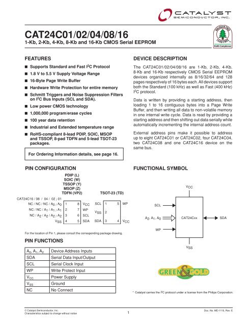
PIN CONFIGURATION FUNCTIONAL SYMBOL<br />
PDIP (L)<br />
SOIC (W)<br />
TSSOP (Y)<br />
MSOP (Z)<br />
TDFN (VP2)<br />
CAT24C<strong>16</strong> / 08 / 04 / 02 / 01<br />
NC / NC / NC / A0 / A0 1 8 VCC NC / NC / A1 / A1 / A1 2 7 WP<br />
NC / A2 / A2 / A2 / A2 3 6 SCL<br />
VSS 4 5 SDA<br />
For the location of Pin 1, please consult the corresponding package drawing.<br />
PIN FUNCTIONS<br />
A0, A1, A2 Device Address Inputs<br />
SDA <strong>Serial</strong> Data Input/Output<br />
SCL <strong>Serial</strong> Clock Input<br />
WP Write Protect Input<br />
VCC Power Supply<br />
VSS Ground<br />
NC No Connect<br />
© Catalyst Semiconductor, Inc.<br />
Characteristics subject to change without notice<br />
SCL<br />
V SS<br />
SDA<br />
TSOT-23 (TD)<br />
1<br />
2<br />
3<br />
5<br />
4<br />
WP<br />
V CC<br />
1<br />
DEVICE DESCRIPTION<br />
The CAT24C01/02/04/08/<strong>16</strong> are 1-<strong>Kb</strong>, 2-<strong>Kb</strong>, 4-<strong>Kb</strong>,<br />
8-<strong>Kb</strong> <strong>and</strong> <strong>16</strong>-<strong>Kb</strong> respectively <strong>CMOS</strong> <strong>Serial</strong> <strong>EEPROM</strong><br />
devices organized internally as 8/<strong>16</strong>/32/64 <strong>and</strong> 128<br />
pages respectively of <strong>16</strong> bytes each. All devices support<br />
both the St<strong>and</strong>ard (100 kHz) as well as Fast (400 kHz)<br />
I 2 C protocol.<br />
Data is written by providing a starting address, then<br />
loading 1 to <strong>16</strong> contiguous bytes into a Page Write<br />
Buffer, <strong>and</strong> then writing all data to non-volatile memory<br />
in one internal write cycle. Data is read by providing a<br />
starting address <strong>and</strong> then shifting out data serially while<br />
automatically incrementing the internal address count.<br />
External address pins make it possible to address<br />
up to eight CAT24C01 or CAT24C02, four CAT24C04,<br />
two CAT24C08 <strong>and</strong> one CAT24C<strong>16</strong> device on the<br />
same bus.<br />
SCL<br />
A 2 , A 1 , A 0<br />
WP<br />
VCC<br />
CAT24Cxx<br />
VSS<br />
SDA<br />
* Catalyst carries the I 2 C protocol under a license from the Philips Corporation.<br />
Doc. No. MD-1115, Rev. E
CAT24C01/02/04/08/<strong>16</strong><br />
ABSOLUTE MAXIMUM RATINGS (1)<br />
Storage Temperature -65°C to +150°C<br />
Voltage on Any Pin with Respect to Ground (2) -0.5 V to +6.5 V<br />
RELIABILITY CHARACTERISTICS (3)<br />
Symbol Parameter Min Units<br />
N END (4) Endurance 1,000,000 Program/ Erase Cycles<br />
T DR Data Retention 100 Years<br />
D.C. OPERATING CHARACTERISTICS<br />
V CC = 1.8 V to 5.5 V, T A = -40°C to +125°C, unless otherwise specified.<br />
Symbol Parameter Test Conditions Min Max Units<br />
I CCR Read Current Read, f SCL = 400kHz 1 mA<br />
I CCW Write Current Write, f SCL = 400kHz 2 mA<br />
I SB St<strong>and</strong>by Current All I/O Pins at GND or V CC<br />
I L I/O Pin Leakage Pin at GND or V CC<br />
Doc. No. MD-1115, Rev. E<br />
2<br />
T A = -40°C to +85°C 1<br />
T A = -40°C to +125°C 2<br />
T A = -40°C to +85°C 1<br />
T A = -40°C to +125°C 2<br />
V IL Input Low Voltage -0.5 V CC x 0.3 V<br />
V IH Input High Voltage V CC x 0.7 V CC + 0.5 V<br />
V OL1 Output Low Voltage V CC < 2.5 V, I OL = 3.0mA 0.4 V<br />
V OL2 Output Low Voltage V CC < 2.5 V, I OL = 1.0mA 0.2 V<br />
PIN IMPEDANCE CHARACTERISTICS<br />
V CC = 1.8 V to 5.5 V, T A = -40°C to +125°C, unless otherwise specified.<br />
Symbol Parameter Conditions Max Units<br />
C IN (3) SDA I/O Pin Capacitance V IN = 0 V 8 pF<br />
C IN (3) Input Capacitance (other pins) V IN = 0 V 6 pF<br />
I WP (5) WP Input Current VIN < V IH, V CC = 5.5 V 200<br />
V IN < V IH, V CC = 3.3 V 150<br />
V IN < V IH, V CC = 1.8 V 100<br />
V IN > V IH<br />
Note:<br />
(1) Stresses above those listed under “Absolute Maximum Ratings” may cause permanent damage to the device. These are stress ratings<br />
only, <strong>and</strong> functional operation of the device at these or any other conditions outside of those listed in the operational sections of this specification<br />
is not implied. Exposure to any absolute maximum rating for extended periods may affect device performance <strong>and</strong> reliability.<br />
(2) The DC input voltage on any pin should not be lower than -0.5 V or higher than VCC + 0.5 V. During transitions, the voltage on any pin may<br />
undershoot to no less than -1.5 V or overshoot to no more than VCC + 1.5 V, for periods of less than 20 ns.<br />
(3) These parameters are tested initially <strong>and</strong> after a design or process change that affects the parameter according to appropriate AEC-Q100<br />
<strong>and</strong> JEDEC test methods.<br />
(4) Page Mode, VCC = 5 V, 25°C<br />
(5) When not driven, the WP pin is pulled down to GND internally. For improved noise immunity, the internal pull-down is relatively strong;<br />
therefore the external driver must be able to supply the pull-down current when attempting to drive the input HIGH. To conserve power,<br />
as the input level exceeds the trip point of the <strong>CMOS</strong> input buffer (~ 0.5 x VCC), the strong pull-down reverts to a weak current source.<br />
1<br />
μA<br />
μA<br />
μA<br />
© Catalyst Semiconductor, Inc.<br />
Characteristics subject to change without notice
A.C. CHARACTERISTICS (1)<br />
V CC = 1.8 V to 5.5 V, T A = -40°C to +125°C.<br />
Symbol Parameter<br />
© Catalyst Semiconductor, Inc.<br />
Characteristics subject to change without notice<br />
3<br />
St<strong>and</strong>ard Fast<br />
Min Max Min Max<br />
CAT24C01/02/04/08/<strong>16</strong><br />
F SCL Clock Frequency 100 400 kHz<br />
t HD:STA START Condition Hold Time 4 0.6 μs<br />
t LOW Low Period of SCL Clock 4.7 1.3 μs<br />
t HIGH High Period of SCL Clock 4 0.6 μs<br />
t SU:STA START Condition Setup Time 4.7 0.6 μs<br />
t HD:DAT Data In Hold Time 0 0 μs<br />
t SU:DAT Data In Setup Time 250 100 ns<br />
t R SDA <strong>and</strong> SCL Rise Time 1000 300 ns<br />
t F (2) SDA <strong>and</strong> SCL Fall Time 300 300 ns<br />
t SU:STO STOP Condition Setup Time 4 0.6 μs<br />
t BUF Bus Free Time Between STOP <strong>and</strong> START 4.7 1.3 μs<br />
t AA SCL Low to Data Out Valid 3.5 0.9 μs<br />
t DH Data Out Hold Time 100 100 ns<br />
T i (2) Noise Pulse Filtered at SCL <strong>and</strong> SDA Inputs 100 100 ns<br />
t SU:WP WP Setup Time 0 0 μs<br />
t HD:WP WP Hold Time 2.5 2.5 μs<br />
t WR Write Cycle Time 5 5 ms<br />
t PU (2, 3) Power-up to Ready Mode 1 1 ms<br />
Note:<br />
(1) Test conditions according to “A.C. Test Conditions” table.<br />
(2) Tested initially <strong>and</strong> after a design or process change that affects this parameter.<br />
(3) tPU is the delay between the time VCC is stable <strong>and</strong> the device is ready to accept comm<strong>and</strong>s.<br />
A.C. TEST CONDITIONS<br />
Input Levels 0.2 x VCC to 0.8 x VCC Input Rise <strong>and</strong> Fall Times ≤ 50 ns<br />
Input Reference Levels 0.3 x VCC, 0.7 x VCC Output Reference Levels 0.5 x VCC Output Load Current Source: I OL = 3 mA (V CC ≥ 2.5 V); I OL = 1 mA (V CC < 2.5 V); C L = 100 pF<br />
Units<br />
Doc No. MD-1115, Rev. E
CAT24C01/02/04/08/<strong>16</strong><br />
POWER-ON RESET (POR)<br />
Each CAT24Cxx* incorporates Power-On Reset (POR)<br />
circuitry which protects the internal logic against<br />
powering up in the wrong state.<br />
A CAT24Cxx device will power up into St<strong>and</strong>by mode<br />
after V CC exceeds the POR trigger level <strong>and</strong> will power<br />
down into Reset mode when V CC drops below the POR<br />
trigger level. This bi-directional POR feature protects<br />
the device against ‘brown-out’ failure following a<br />
temporary loss of power.<br />
* For common features, the CAT24C01/02/04/08/<strong>16</strong> will be refered<br />
to as CAT24Cxx<br />
PIN DESCRIPTION<br />
SCL: The <strong>Serial</strong> Clock input pin accepts the <strong>Serial</strong> Clock<br />
generated by the Master.<br />
SDA: The <strong>Serial</strong> Data I/O pin receives input data <strong>and</strong><br />
transmits data stored in <strong>EEPROM</strong>. In transmit mode, this<br />
pin is open drain. Data is acquired on the positive edge,<br />
<strong>and</strong> is delivered on the negative edge of SCL.<br />
A0, A1 <strong>and</strong> A2: The Address inputs set the device address<br />
when cascading multiple devices. When not driven,<br />
these pins are pulled LOW internally.<br />
WP: The Write Protect input pin inhibits all write operations,<br />
when pulled HIGH. When not driven, this pin is<br />
pulled LOW internally.<br />
FUNCTIONAL DESCRIPTION<br />
The CAT24Cxx supports the Inter-Integrated Circuit (I 2 C)<br />
Bus data transmission protocol, which defines a device<br />
that sends data to the bus as a transmitter <strong>and</strong> a device<br />
receiving data as a receiver. Data flow is controlled by<br />
a Master device, which generates the serial clock <strong>and</strong><br />
all START <strong>and</strong> STOP conditions. The CAT24Cxx acts<br />
as a Slave device. Master <strong>and</strong> Slave alternate as either<br />
transmitter or receiver.<br />
Doc. No. MD-1115, Rev. E<br />
4<br />
I 2 C BUS PROTOCOL<br />
The I 2 C bus consists of two ‘wires’, SCL <strong>and</strong> SDA. The<br />
two wires are connected to the V CC supply via pull-up<br />
resistors. Master <strong>and</strong> Slave devices connect to the 2wire<br />
bus via their respective SCL <strong>and</strong> SDA pins. The<br />
transmitting device pulls down the SDA line to ‘transmit’<br />
a ‘0’ <strong>and</strong> releases it to ‘transmit’ a ‘1’.<br />
Data transfer may be initiated only when the bus is not<br />
busy (see A.C. Characteristics).<br />
During data transfer, the SDA line must remain stable<br />
while the SCL line is HIGH. An SDA transition while<br />
SCL is HIGH will be interpreted as a START or STOP<br />
condition (Figure 1). The START condition precedes all<br />
comm<strong>and</strong>s. It consists of a HIGH to LOW transition on<br />
SDA while SCL is HIGH. The START acts as a ‘wake-up’<br />
call to all receivers. Absent a START, a Slave will not<br />
respond to comm<strong>and</strong>s. The STOP condition completes<br />
all comm<strong>and</strong>s. It consists of a LOW to HIGH transition<br />
on SDA while SCL is HIGH.<br />
Device Addressing<br />
The Master initiates data transfer by creating a START<br />
condition on the bus. The Master then broadcasts an<br />
8-bit serial Slave address. For normal Read/Write operations,<br />
the first 4 bits of the Slave address are fixed at<br />
1010 (Ah). The next 3 bits are used as programmable<br />
address bits when cascading multiple devices <strong>and</strong>/or as<br />
internal address bits. The last bit of the slave address,<br />
R/W, specifies whether a Read (1) or Write (0) operation<br />
is to be performed. The 3 address space extension bits<br />
are assigned as illustrated in Figure 2. A2, A1 <strong>and</strong> A0 must match the state of the external address pins, <strong>and</strong><br />
a10, a9 <strong>and</strong> a8 are internal address bits.<br />
Acknowledge<br />
After processing the Slave address, the Slave responds<br />
with an acknowledge (ACK) by pulling down the SDA<br />
line during the 9th clock cycle (Figure 3). The Slave will<br />
also acknowledge the address byte <strong>and</strong> every data byte<br />
presented in Write mode. In Read mode the Slave shifts<br />
out a data byte, <strong>and</strong> then releases the SDA line during<br />
the 9th clock cycle. As long as the Master acknowledges<br />
the data, the Slave will continue transmitting. The Master<br />
terminates the session by not acknowledging the last<br />
data byte (NoACK) <strong>and</strong> by issuing a STOP condition.<br />
Bus timing is illustrated in Figure 4.<br />
© Catalyst Semiconductor, Inc.<br />
Characteristics subject to change without notice
Figure 1. START/STOP Conditions<br />
SCL<br />
SDA<br />
Figure 2. Slave Address Bits<br />
Figure 3. Acknowledge Timing<br />
SCL FROM<br />
MASTER<br />
DATA OUTPUT<br />
FROM TRANSMITTER<br />
DATA OUTPUT<br />
FROM RECEIVER<br />
Figure 4. Bus Timing<br />
SCL<br />
SDA IN<br />
SDA OUT<br />
t SU:STA<br />
START<br />
© Catalyst Semiconductor, Inc.<br />
Characteristics subject to change without notice<br />
START<br />
CONDITION<br />
1 8 9<br />
5<br />
CAT24C01/02/04/08/<strong>16</strong><br />
BUS RELEASE DELAY (TRANSMITTER) BUS RELEASE DELAY (RECEIVER)<br />
ACK DELAY (≤ tAA)<br />
t HIGH<br />
STOP<br />
CONDITION<br />
1 0 1 0 A2 A1 A0 R/W CAT24C01 <strong>and</strong> CAT24C02<br />
1 0 1 0 A 2 A 1 a 8 R/W CAT24C04<br />
1 0 1 0 A 2 a 9 a 8 R/W CAT24C08<br />
1 0 1 0 a10 a9 a8 R/W CAT24C<strong>16</strong><br />
t F<br />
t LOW<br />
t HD:STA<br />
t AA<br />
t HD:DAT<br />
t LOW<br />
t DH<br />
t R<br />
t SU:DAT<br />
ACK SETUP (≥ t SU:DAT )<br />
t SU:STO<br />
t BUF<br />
Doc No. MD-1115, Rev. E
CAT24C01/02/04/08/<strong>16</strong><br />
WRITE OPERATIONS<br />
Byte Write<br />
In Byte Write mode, the Master sends the START condition<br />
<strong>and</strong> the Slave address with the R/W bit set to zero<br />
to the Slave. After the Slave generates an acknowledge,<br />
the Master sends the byte address that is to be written<br />
into the address pointer of the CAT24Cxx. After receiving<br />
another acknowledge from the Slave, the Master<br />
transmits the data byte to be written into the addressed<br />
memory location. The CAT24Cxx device will acknowledge<br />
the data byte <strong>and</strong> the Master generates the STOP<br />
condition, at which time the device begins its internal<br />
Write cycle to nonvolatile memory (Figure 5). While this<br />
internal cycle is in progress (tWR), the SDA output will<br />
be tri-stated <strong>and</strong> the CAT24Cxx will not respond to any<br />
request from the Master device (Figure 6).<br />
Page Write<br />
The CAT24Cxx writes up to <strong>16</strong> bytes of data in a single<br />
write cycle, using the Page Write operation (Figure 7).<br />
The Page Write operation is initiated in the same manner<br />
as the Byte Write operation, however instead of terminating<br />
after the data byte is transmitted, the Master is<br />
allowed to send up to fifteen additional bytes. After each<br />
byte has been transmitted the CAT24Cxx will respond<br />
with an acknowledge <strong>and</strong> internally increments the four<br />
low order address bits. The high order bits that define<br />
the page address remain unchanged. If the Master<br />
transmits more than sixteen bytes prior to sending the<br />
STOP condition, the address counter ‘wraps around’ to<br />
the beginning of page <strong>and</strong> previously transmitted data<br />
will be overwritten. Once all sixteen bytes are received<br />
<strong>and</strong> the STOP condition has been sent by the Master,<br />
the internal Write cycle begins. At this point all received<br />
data is written to the CAT24Cxx in a single write cycle.<br />
Acknowledge Polling<br />
The acknowledge (ACK) polling routine can be used to<br />
take advantage of the typical write cycle time. Once the<br />
stop condition is issued to indicate the end of the host’s<br />
write operation, the CAT24Cxx initiates the internal write<br />
cycle. The ACK polling can be initiated immediately. This<br />
involves issuing the start condition followed by the slave<br />
address for a write operation. If the CAT24Cxx is still<br />
busy with the write operation, NoACK will be returned. If<br />
the CAT24Cxx has completed the internal write operation,<br />
an ACK will be returned <strong>and</strong> the host can then proceed<br />
with the next read or write operation.<br />
Doc. No. MD-1115, Rev. E<br />
6<br />
Hardware Write Protection<br />
With the WP pin held HIGH, the entire memory is protected<br />
against Write operations. If the WP pin is left floating or<br />
is grounded, it has no impact on the operation of the<br />
CAT24Cxx. The state of the WP pin is strobed on the<br />
last falling edge of SCL immediately preceding the first<br />
data byte (Figure 8). If the WP pin is HIGH during the<br />
strobe interval, the CAT24Cxx will not acknowledge the<br />
data byte <strong>and</strong> the Write request will be rejected.<br />
Delivery State<br />
The CAT24Cxx is shipped erased, i.e., all bytes are<br />
FFh.<br />
© Catalyst Semiconductor, Inc.<br />
Characteristics subject to change without notice
Figure 5. Byte Write Sequence<br />
Figure 6. Write Cycle Timing<br />
SCL<br />
SDA<br />
Figure 7. Page Write Sequence<br />
BUS ACTIVITY:<br />
MASTER<br />
SLAVE<br />
Figure 8. WP Timing<br />
BUS ACTIVITY:<br />
S<br />
T<br />
A<br />
R T<br />
© Catalyst Semiconductor, Inc.<br />
Characteristics subject to change without notice<br />
S<br />
n = 1<br />
P ≤ 15<br />
SCL<br />
SDA<br />
WP<br />
MASTER<br />
8 th Bit<br />
Byte n<br />
SLAVE<br />
ADDRESS<br />
S<br />
T<br />
A<br />
R<br />
T<br />
S<br />
A<br />
C<br />
K<br />
SLAVE<br />
ADDRESS<br />
A<br />
SLAVE<br />
C<br />
K<br />
* For the CAT24C01 a7 = 0<br />
ADDRESS<br />
BYTE<br />
ACK<br />
ADDRESS<br />
BYTE<br />
A<br />
C<br />
K<br />
STOP<br />
CONDITION<br />
7<br />
ADDRESS<br />
BYTE<br />
a7 ÷ a0<br />
DATA<br />
BYTE<br />
n<br />
A<br />
C<br />
K<br />
t WR<br />
A<br />
C<br />
K<br />
DATA<br />
BYTE<br />
d7 ÷ d0<br />
DATA<br />
BYTE<br />
n+1<br />
A<br />
C<br />
K<br />
START<br />
CONDITION<br />
1 8 9 1 8<br />
a7 a0 d7 d0<br />
tSU:WP<br />
tHD:WP<br />
DATA<br />
BYTE<br />
A<br />
C<br />
K<br />
CAT24C01/02/04/08/<strong>16</strong><br />
S<br />
T<br />
O<br />
P<br />
P<br />
DATA<br />
BYTE<br />
n+P<br />
ADDRESS<br />
A<br />
C K<br />
S T<br />
O P<br />
P<br />
Doc No. MD-1115, Rev. E
CAT24C01/02/04/08/<strong>16</strong><br />
READ OPERATIONS<br />
Immediate Read<br />
Upon receiving a Slave address with the R/W bit set<br />
to ‘1’, the CAT24Cxx will interpret this as a request for<br />
data residing at the current byte address in memory.<br />
The CAT24Cxx will acknowledge the Slave address,<br />
will immediately shift out the data residing at the current<br />
address, <strong>and</strong> will then wait for the Master to respond.<br />
If the Master does not acknowledge the data (NoACK)<br />
<strong>and</strong> then follows up with a STOP condition (Figure 9),<br />
the CAT24Cxx returns to St<strong>and</strong>by mode.<br />
Selective Read<br />
Selective Read operations allow the Master device to<br />
select at r<strong>and</strong>om any memory location for a read operation.<br />
The Master device first performs a ‘dummy’ write<br />
operation by sending the START condition, slave address<br />
<strong>and</strong> byte address of the location it wishes to read.<br />
After the CAT24Cxx acknowledges the byte address,<br />
the Master device resends the START condition <strong>and</strong><br />
the slave address, this time with the R/W bit set to one.<br />
The CAT24Cxx then responds with its acknowledge <strong>and</strong><br />
sends the requested data byte. The Master device does<br />
not acknowledge the data (NoACK) but will generate a<br />
STOP condition (Figure 10).<br />
Sequential Read<br />
If during a Read session, the Master acknowledges the 1st data byte, then the CAT24Cxx will continue transmitting<br />
data residing at subsequent locations until the Master<br />
responds with a NoACK, followed by a STOP (Figure<br />
11). In contrast to Page Write, during Sequential Read<br />
the address count will automatically increment to <strong>and</strong><br />
then wrap-around at end of memory (rather than end<br />
of page). In the CAT24C01, the internal address count<br />
will not wrap around at the end of the 128 byte memory<br />
space.<br />
Doc. No. MD-1115, Rev. E<br />
8<br />
© Catalyst Semiconductor, Inc.<br />
Characteristics subject to change without notice
Figure 9. Immediate Read Sequence <strong>and</strong> Timing<br />
SCL<br />
Figure 10. Selective Read Sequence<br />
Figure 11. Sequential Read Sequence<br />
BUS ACTIVITY:<br />
MASTER<br />
SLAVE<br />
BUS ACTIVITY:<br />
MASTER<br />
SLAVE<br />
SLAVE<br />
ADDRESS<br />
© Catalyst Semiconductor, Inc.<br />
Characteristics subject to change without notice<br />
BUS ACTIVITY:<br />
S<br />
T<br />
A<br />
R<br />
T<br />
S<br />
A<br />
C<br />
K<br />
MASTER<br />
SLAVE<br />
SDA 8th Bit<br />
SLAVE<br />
ADDRESS<br />
DATA<br />
BYTE<br />
n<br />
S<br />
T<br />
A<br />
R<br />
T<br />
S<br />
DATA OUT<br />
A<br />
C K<br />
A<br />
C<br />
K<br />
SLAVE<br />
ADDRESS<br />
8 9<br />
ADDRESS<br />
BYTE<br />
DATA<br />
BYTE<br />
n+1<br />
9<br />
A<br />
C<br />
K<br />
NO ACK<br />
A<br />
C K<br />
A<br />
C<br />
K<br />
S<br />
T<br />
A<br />
R<br />
T<br />
S<br />
DATA<br />
BYTE<br />
SLAVE<br />
ADDRESS<br />
DATA<br />
BYTE<br />
n+2<br />
N<br />
O<br />
S<br />
A T<br />
C O<br />
K P<br />
P<br />
A<br />
C<br />
K<br />
A<br />
C K<br />
CAT24C01/02/04/08/<strong>16</strong><br />
STOP<br />
DATA<br />
BYTE<br />
DATA<br />
BYTE<br />
n+x<br />
N<br />
O<br />
S<br />
A T<br />
C O<br />
K P<br />
P<br />
N<br />
O<br />
S<br />
A T<br />
C O<br />
K P<br />
P<br />
Doc No. MD-1115, Rev. E
CAT24C01/02/04/08/<strong>16</strong><br />
PACKAGE PDIP 8-Lead DIMENSIONS 300mils (L)<br />
PDIP 8-Lead 300 MIL (L)<br />
A<br />
L<br />
Doc. No. MD-1115, Rev. E<br />
PIN # 1<br />
IDENTIFICATION<br />
D<br />
TOP VIEW<br />
e b<br />
b2<br />
A2<br />
A1<br />
E1<br />
SIDE VIEW END VIEW<br />
10<br />
PACKAGE INFORMATION<br />
SYMBOL MIN NOM MAX<br />
A 5.33<br />
A1 0.38<br />
A2 2.92 3.30 4.95<br />
b 0.36 0.46 0.56<br />
b2 1.14 1.52 1.78<br />
c 0.20 0.25 0.36<br />
D 9.02 9.27 10.<strong>16</strong><br />
E 7.62 7.87 8.25<br />
e 2.54 BSC<br />
E1 6.10 6.35 7.11<br />
eB 7.87 10.92<br />
L 2.92 3.30 3.80<br />
For current Tape <strong>and</strong> Reel information, download the PDF file from:<br />
http://www.catsemi.com/documents/tape<strong>and</strong>reel.pdf.<br />
Notes:<br />
Notes: (1) All dimensions are in millimeters.<br />
(1) (2) All dimensions Complies with are JEDEC in millimeters. MS-001.<br />
(2) Complies with JEDEC MS-001.<br />
E<br />
eB<br />
Doc. No. PDIP8-001-01<br />
06/20/07<br />
© Catalyst Semiconductor, Inc.<br />
Characteristics subject to change without notice<br />
c
SOIC 8-Lead 150 mils (V, W)<br />
SOIC 8-Lead 150 MIL (W)<br />
PIN # 1<br />
IDENTIFICATION<br />
A<br />
TOP VIEW<br />
e b<br />
© Catalyst Semiconductor, Inc.<br />
Characteristics subject to change without notice<br />
D<br />
A1<br />
E1 E<br />
SIDE VIEW END VIEW<br />
For current Tape <strong>and</strong> Reel information, download the PDF file from:<br />
Notes:<br />
http://www.catsemi.com/documents/tape<strong>and</strong>reel.pdf.<br />
(1) All dimensions are in millimeters. Angles in degrees.<br />
(2) Complies with JEDEC MS-012.<br />
Notes:<br />
(1) All dimensions are in millimeters. Angles in degrees.<br />
(2) Complies with JEDEC MS-012.<br />
11<br />
θ<br />
L<br />
h<br />
PACKAGE CAT24C01/02/04/08/<strong>16</strong><br />
INFORMATION<br />
SYMBOL MIN NOM MAX<br />
A 1.35 1.75<br />
A1 0.10 0.25<br />
b 0.33 0.51<br />
c 0.19 0.25<br />
D 4.80 5.00<br />
E 5.80 6.20<br />
E1 3.80 4.00<br />
e 1.27 BSC<br />
h 0.25 0.50<br />
L 0.40 1.27<br />
θ 0º 8º<br />
Doc. No. SOIC8-002-01<br />
06.20.2007<br />
c<br />
Doc No. MD-1115, Rev. E
CAT24C01/02/04/08/<strong>16</strong><br />
TSSOP 8-Lead 4.4mm (U, Y)<br />
TSSOP 8-Lead (Y)<br />
A2<br />
e<br />
Doc. No. MD-1115, Rev. E<br />
TOP VIEW<br />
D<br />
b<br />
A1<br />
E1 E<br />
A<br />
SIDE VIEW END VIEW<br />
For current Tape <strong>and</strong> Reel information, download the PDF file from:<br />
Notes:<br />
http://www.catsemi.com/documents/tape<strong>and</strong>reel.pdf.<br />
(1) All dimensions are in millimeters. Angles in degrees.<br />
(2) Complies with JEDEC MO-153.<br />
Notes:<br />
(1) All dimensions are in millimeters.<br />
(2) Complies with JEDEC MO-153.<br />
θ1<br />
L1<br />
12<br />
PACKAGE OUTLINE DRAWING<br />
SYMBOL MIN NOM MAX<br />
A 1.20<br />
A1 0.05 0.15<br />
A2 0.80 0.90 1.05<br />
b 0.19 0.30<br />
c 0.09 0.20<br />
D 2.90 3.00 3.10<br />
E 6.30 6.40 6.50<br />
E1 4.30 4.40 4.50<br />
e 0.65 BSC<br />
L 1.00 REF<br />
L1 0.50 0.60 0.75<br />
θ1 0° 8°<br />
© Catalyst Semiconductor, Inc.<br />
Characteristics subject to change without notice<br />
L<br />
Doc. No. TSSOP8-004-01<br />
06/21/07<br />
c
MSOP 8-Lead (Z)<br />
MSOP 8-Lead 3.0mm (R, Z)<br />
E<br />
A<br />
E1<br />
A2<br />
TOP VIEW<br />
A1 e b<br />
For current Tape <strong>and</strong> Reel information,<br />
download the PDF file from:<br />
http://www.catsemi.com/documents/tape<strong>and</strong>reel.pdf.<br />
Notes:<br />
(1)<br />
Notes:<br />
All dimensions are in millimeters. Angles in degrees.<br />
(2)<br />
(1)<br />
Complies<br />
All dimensions<br />
with JEDEC<br />
are in millimeters.<br />
MO-187.<br />
Angels in degrees.<br />
(2) Complies with JEDEC specification MS-187.<br />
(3) St<strong>and</strong> off height/coplanarity are considered as special characteristics.<br />
© Catalyst Semiconductor, Inc.<br />
Characteristics subject to change without notice<br />
D<br />
c<br />
SIDE VIEW END VIEW<br />
13<br />
CAT24C01/02/04/08/<strong>16</strong><br />
PACKAGE OUTLINE DRAWING<br />
SYMBOL MIN NOM MAX<br />
A 1.10<br />
A1 0.05 0.10 0.15<br />
A2 0.75 0.85 0.95<br />
b 0.28 0.33 0.38<br />
c 0.13 0.23<br />
D 2.90 3.00 3.10<br />
E 4.80 4.90 5.00<br />
E1 2.90 3.00 3.10<br />
e 0.65 BSC<br />
L 0.40 0.60 0.80<br />
L1 0.95 REF<br />
L2 0.25 BSC<br />
θ 0º 6º<br />
DETAIL A<br />
L1<br />
L<br />
θ<br />
L2<br />
DETAIL A<br />
Doc. No. MSOP8-003-01<br />
06/20/07<br />
Doc No. MD-1115, Rev. E
CAT24C01/02/04/08/<strong>16</strong><br />
TDFN 8-Pad 8-Lead 2 x 3mm 2 x 3mm (VP2) (SP2, VP2)<br />
D<br />
For current Tape <strong>and</strong> Reel information, download the PDF file from:<br />
http://www.catsemi.com/documents/tape<strong>and</strong>reel.pdf.<br />
Notes:<br />
(1) All dimensions are in millimeters.<br />
Notes:<br />
(1) All dimensions are in millimeters. Angels in degrees.<br />
(2) Complies with JEDEC specification MO-229.<br />
Doc. No. MD-1115, Rev. E<br />
PIN#1 INDEX AREA<br />
E<br />
14<br />
E2<br />
A2<br />
e b<br />
TOP VIEW SIDE VIEW BOTTOM VIEW<br />
SYMBOL MIN NOM MAX<br />
A 0.70 0.75 0.80<br />
A1 0.00 0.02 0.05<br />
A2 0.45 0.55 0.65<br />
A3 0.20 REF<br />
b 0.20 0.25 0.30<br />
D 1.90 2.00 2.10<br />
D2 1.30 1.40 1.50<br />
E 2.90 3.00 3.10<br />
E2 1.20 1.30 1.40<br />
e 050 TYP<br />
L 0.20 0.30 0.40<br />
(2) Complies with JEDEC MO-229.<br />
A<br />
A1<br />
PACKAGE OUTLINE DRAWING<br />
D2<br />
FRONT VIEW<br />
L<br />
A3<br />
PIN#1<br />
IDENTIFICATION<br />
Doc. No. TDFN8-008-01<br />
06/21/07<br />
© Catalyst Semiconductor, Inc.<br />
Characteristics subject to change without notice
TSOT-23 5-Lead (TD)<br />
TSOT-23 5-Lead (TD)<br />
Notes:<br />
For current Tape <strong>and</strong> Reel information, download the PDF file from:<br />
(1) All dimensions are in millimeters. Angles in degrees.<br />
(2) Complies with JEDEC http://www.catsemi.com/documents/tape<strong>and</strong>reel.pdf.<br />
MO-193.<br />
Notes:<br />
(1) All dimensions are in millimeters. Angels in degrees.<br />
(2) Complies with JEDEC specification MO-193.<br />
© Catalyst Semiconductor, Inc.<br />
Characteristics subject to change without notice<br />
e<br />
D<br />
TOP VIEW<br />
b<br />
E1 E<br />
A2 A<br />
A1<br />
SIDE VIEW END VIEW<br />
15<br />
L1<br />
L<br />
PACKAGE INFORMATION<br />
CAT24C01/02/04/08/<strong>16</strong><br />
c<br />
L2<br />
Doc. No. TSOP235-005-01<br />
06/20/07<br />
Doc No. MD-1115, Rev. E
CAT24C01/02/04/08/<strong>16</strong><br />
EXAMPLE OF ORDERING INFORMATION<br />
Prefix Device # Suffix<br />
CAT<br />
Notes:<br />
(1) All packages are RoHS-compliant (Lead-free, Halogen-free).<br />
(2) The st<strong>and</strong>ard lead finish is NiPdAu pre-plated (PPF) lead frames.<br />
(3) The device used in the above example is a CAT24C<strong>16</strong>YI-GT3 (TSSOP, Industrial Temperature, NiPdAu, Tape & Reel).<br />
(4) For availability, please contact your nearest Catalyst Semiconductor Sales Office.<br />
(5) For additional package <strong>and</strong> temperature options, please contact your nearest Catalyst Semiconductor Sales office.<br />
Doc. No. MD-1115, Rev. E<br />
24C<strong>16</strong> Y I – G T3<br />
Company ID Product Number<br />
T: Tape & Reel<br />
24C01<br />
3: 3000/Reel<br />
24C02<br />
24C04<br />
24C08<br />
24C<strong>16</strong><br />
Package<br />
L: PDIP<br />
W: SOIC, JEDEC<br />
Y: TSSOP<br />
Z: MSOP (4)<br />
Temperature Range<br />
I = Industrial (-40°C to +85°C)<br />
E = Extended (-40°C to +125°C)<br />
Lead Finish<br />
G: NiPdAu<br />
Blank: Matte-Tin<br />
VP2: TDFN<br />
TD: TSOT<br />
<strong>16</strong><br />
© Catalyst Semiconductor, Inc.<br />
Characteristics subject to change without notice
REVISION HISTORY<br />
Date Revision Comments<br />
07/18/06 A Combine 5 data sheets into one data sheet.<br />
07/31/06 B Update Package Marking<br />
11/29/06 C Update Features<br />
Update Pin Configuration<br />
Update Functional Symbol<br />
Added 8-Lead MSOP Package Outline<br />
Remove Package Marking<br />
Update Example of Ordering Information<br />
06/14/07 D<br />
Copyrights, Trademarks <strong>and</strong> Patents<br />
© Catalyst Semiconductor, Inc.<br />
Trademarks <strong>and</strong> registered trademarks of Catalyst Semiconductor include each of the following:<br />
Beyond Memory , DPP , EZDim , LDD , MiniPot <strong>and</strong> Quad-Mode<br />
Catalyst Semiconductor has been issued U.S. <strong>and</strong> foreign patents <strong>and</strong> has patent applications pending that protect its products.<br />
CATALYST SEMICONDUCTOR MAKES NO WARRANTY, REPRESENTATION OR GUARANTEE, EXPRESS OR IMPLIED, REGARDING THE SUITABILITY OF ITS<br />
PRODUCTS FOR ANY PARTICULAR PURPOSE, NOR THAT THE USE OF ITS PRODUCTS WILL NOT INFRINGE ITS INTELLECTUAL PROPERTY RIGHTS OR THE<br />
RIGHTS OF THIRD PARTIES WITH RESPECT TO ANY PARTICULAR USE OR APPLICATION AND SPECIFICALLY DISCLAIMS ANY AND ALL LIABILITY ARISING<br />
OUT OF ANY SUCH USE OR APPLICATION, INCLUDING BUT NOT LIMITED TO, CONSEQUENTIAL OR INCIDENTAL DAMAGES.<br />
Catalyst Semiconductor products are not designed, intended, or authorized for use as components in systems intended for surgical implant into the body, or other<br />
applications intended to support or sustain life, or for any other application in which the failure of the Catalyst Semiconductor product could create a situation<br />
where personal injury or death may occur.<br />
Catalyst Semiconductor reserves the right to make changes to or discontinue any product or service described herein without notice. Products with data sheets<br />
labeled “Advance Information” or “Preliminary” <strong>and</strong> other products described herein may not be in production or offered for sale.<br />
Catalyst Semiconductor advises customers to obtain the current version of the relevant product information before placing orders. Circuit diagrams illustrate typical<br />
semiconductor applications <strong>and</strong> may not be complete.<br />
Catalyst Semiconductor, Inc.<br />
Corporate Headquarters<br />
2975 Stender Way<br />
Santa Clara, CA 95054<br />
Phone: 408.542.1000<br />
Fax: 408.542.1200<br />
www.catsemi.com<br />
Update PDIP 8-Lead 300mils Package Outline<br />
Update document code to include MD-<br />
07/03/07 E Add Extended Temperature range<br />
Update D.C. Operating Characteristics table<br />
Update all Package Outline Drawing<br />
Publication #: MD-1115<br />
Revison: E<br />
Issue date: 07/03/07


![Florian Moraru - Structuri de date [pdf] - Andrei](https://img.yumpu.com/16899682/1/184x260/florian-moraru-structuri-de-date-pdf-andrei.jpg?quality=85)
![Capitolul 2 - Elemente de mecanică cuantică [pdf] - Andrei](https://img.yumpu.com/16899601/1/190x245/capitolul-2-elemente-de-mecanica-cuantica-pdf-andrei.jpg?quality=85)


![Curs 2 - Gestiunea sistemului de fișiere [pdf] - Andrei](https://img.yumpu.com/16899511/1/190x143/curs-2-gestiunea-sistemului-de-fisiere-pdf-andrei.jpg?quality=85)
![Curs 5 - Performanțele circuitelor VLSI [pdf] - Andrei](https://img.yumpu.com/16899506/1/190x245/curs-5-performantele-circuitelor-vlsi-pdf-andrei.jpg?quality=85)