

1-Kb, 2-Kb, 4-Kb, 8-Kb and 16-Kb CMOS Serial EEPROM
1-Kb, 2-Kb, 4-Kb, 8-Kb and 16-Kb CMOS Serial EEPROM
1-Kb, 2-Kb, 4-Kb, 8-Kb and 16-Kb CMOS Serial EEPROM

Create successful ePaper yourself
Turn your PDF publications into a flip-book with our unique Google optimized e-Paper software.
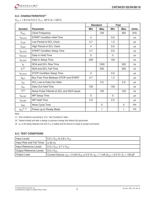
A.C. CHARACTERISTICS (1)<br />
V CC = 1.8 V to 5.5 V, T A = -40°C to +125°C.<br />
Symbol Parameter<br />
© Catalyst Semiconductor, Inc.<br />
Characteristics subject to change without notice<br />
3<br />
St<strong>and</strong>ard Fast<br />
Min Max Min Max<br />
CAT24C01/02/04/08/<strong>16</strong><br />
F SCL Clock Frequency 100 400 kHz<br />
t HD:STA START Condition Hold Time 4 0.6 μs<br />
t LOW Low Period of SCL Clock 4.7 1.3 μs<br />
t HIGH High Period of SCL Clock 4 0.6 μs<br />
t SU:STA START Condition Setup Time 4.7 0.6 μs<br />
t HD:DAT Data In Hold Time 0 0 μs<br />
t SU:DAT Data In Setup Time 250 100 ns<br />
t R SDA <strong>and</strong> SCL Rise Time 1000 300 ns<br />
t F (2) SDA <strong>and</strong> SCL Fall Time 300 300 ns<br />
t SU:STO STOP Condition Setup Time 4 0.6 μs<br />
t BUF Bus Free Time Between STOP <strong>and</strong> START 4.7 1.3 μs<br />
t AA SCL Low to Data Out Valid 3.5 0.9 μs<br />
t DH Data Out Hold Time 100 100 ns<br />
T i (2) Noise Pulse Filtered at SCL <strong>and</strong> SDA Inputs 100 100 ns<br />
t SU:WP WP Setup Time 0 0 μs<br />
t HD:WP WP Hold Time 2.5 2.5 μs<br />
t WR Write Cycle Time 5 5 ms<br />
t PU (2, 3) Power-up to Ready Mode 1 1 ms<br />
Note:<br />
(1) Test conditions according to “A.C. Test Conditions” table.<br />
(2) Tested initially <strong>and</strong> after a design or process change that affects this parameter.<br />
(3) tPU is the delay between the time VCC is stable <strong>and</strong> the device is ready to accept comm<strong>and</strong>s.<br />
A.C. TEST CONDITIONS<br />
Input Levels 0.2 x VCC to 0.8 x VCC Input Rise <strong>and</strong> Fall Times ≤ 50 ns<br />
Input Reference Levels 0.3 x VCC, 0.7 x VCC Output Reference Levels 0.5 x VCC Output Load Current Source: I OL = 3 mA (V CC ≥ 2.5 V); I OL = 1 mA (V CC < 2.5 V); C L = 100 pF<br />
Units<br />
Doc No. MD-1115, Rev. E

![Florian Moraru - Structuri de date [pdf] - Andrei](https://img.yumpu.com/16899682/1/184x260/florian-moraru-structuri-de-date-pdf-andrei.jpg?quality=85)
![Capitolul 2 - Elemente de mecanică cuantică [pdf] - Andrei](https://img.yumpu.com/16899601/1/190x245/capitolul-2-elemente-de-mecanica-cuantica-pdf-andrei.jpg?quality=85)


![Curs 2 - Gestiunea sistemului de fișiere [pdf] - Andrei](https://img.yumpu.com/16899511/1/190x143/curs-2-gestiunea-sistemului-de-fisiere-pdf-andrei.jpg?quality=85)
![Curs 5 - Performanțele circuitelor VLSI [pdf] - Andrei](https://img.yumpu.com/16899506/1/190x245/curs-5-performantele-circuitelor-vlsi-pdf-andrei.jpg?quality=85)