Topic 3 Dielectric Waveguides and Optical Fibers 2-1 Symmetric ...
Topic 3 Dielectric Waveguides and Optical Fibers 2-1 Symmetric ...
Topic 3 Dielectric Waveguides and Optical Fibers 2-1 Symmetric ...

Create successful ePaper yourself
Turn your PDF publications into a flip-book with our unique Google optimized e-Paper software.
901 37500 光電導論<br />
901 37500 光電導論<br />
<strong>Topic</strong> 3<br />
<strong>Dielectric</strong> <strong>Waveguides</strong> <strong>and</strong><br />
<strong>Optical</strong> <strong>Fibers</strong><br />
Kasap Chapter 2<br />
2-1 <strong>Symmetric</strong> Planar <strong>Dielectric</strong><br />
Slab Waveguide<br />
1<br />
3<br />
Contents (Kasap Chapter 2)<br />
1 <strong>Symmetric</strong> Planar <strong>Dielectric</strong> Slab Waveguide<br />
2 Modal <strong>and</strong> Waveguide Dispersion in the Planar Waveguide<br />
3 Step Index Fiber<br />
4 Numerical Aperture<br />
5 Dispersion in Single Mode <strong>Fibers</strong><br />
6 Bit Rate, Dispersion, Electrical <strong>and</strong> <strong>Optical</strong> B<strong>and</strong>width<br />
7 The Graded Index (GRIN) <strong>Optical</strong> Fiber<br />
8 Light Absorption <strong>and</strong> Scattering<br />
9 Attenuation in <strong>Optical</strong> <strong>Fibers</strong><br />
10 Fiber Manufacture<br />
901 37500 光電導論<br />
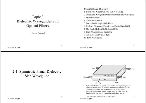
n2 cladding<br />
Light<br />
Light<br />
n2 n1 > n core<br />
2<br />
A planar dielectric waveguide has a central rectangular region of<br />
higher refractive index n1 than the surrounding region which has<br />
a refractive index n2. It is assumed that the waveguide is<br />
infinitely wide <strong>and</strong> the central region is of thickness 2a. It is<br />
illuminated at one end by a monochromatic light source.<br />
901 37500 光電導論<br />
Light<br />
?1999 S.O. Kasap, Optoelectronics (Prentice Hall)<br />
2<br />
Ligh<br />
4
TIR at B & C<br />
k1 (AB+BC) + phase change due to TIR = m(2π)<br />
κ<br />
E<br />
λ<br />
θ<br />
θ θ<br />
?1999 S.O. Kasap, Optoelectronics (Prentice Hall)<br />
901 37500 光電導論<br />
k 1<br />
A<br />
β<br />
B<br />
C<br />
n 2<br />
Light<br />
n 1<br />
n 2<br />
d = 2a<br />
A light ray travelling in the guide must interfere constructively with itself to<br />
propagate successfully. Otherwise destructive interference will destroy the<br />
wave.<br />
1<br />
E<br />
901 37500 光電導論<br />
2<br />
θ<br />
A<br />
k 1<br />
θ<br />
A′<br />
C<br />
n 2<br />
π−2θ<br />
n 1<br />
n 2<br />
B′<br />
2θ−π/2<br />
Two arbitrary waves 1 <strong>and</strong> 2 that are initially in phase must remain in phase<br />
after reflections. Otherwise the two will interfere destructively <strong>and</strong> cancel each<br />
other.<br />
?1999 S.O. Kasap, Optoelectronics (Prentice Hall)<br />
B<br />
θ<br />
2a<br />
y<br />
x<br />
1<br />
y<br />
x<br />
z<br />
z<br />
5<br />
7<br />
901 37500 光電導論<br />
Waveguide Condition<br />
k = kn =<br />
1<br />
1<br />
2 1<br />
π n / λ<br />
For constructive interference, the phase difference between A<br />
<strong>and</strong> C must be a multiple of 2π<br />
Δφ(<br />
AC ) = k ( AB + BC ) − 2φ<br />
= m(<br />
2π<br />
)<br />
1<br />
1<br />
d<br />
BC = AB = BC cos( 2θ<br />
)<br />
cosθ<br />
2<br />
AB + BC = BC cos( 2θ<br />
) + BC = BC[(<br />
2cos<br />
θ −1)<br />
+ 1]<br />
= 2d<br />
cosθ<br />
[ 2d<br />
cosθ<br />
] − 2φ<br />
m(<br />
2π<br />
)<br />
→ k =<br />
Dividing (2) by 2 we obtain the waveguide condition<br />
901 37500 光電導論<br />
⎡<br />
⎢<br />
⎣<br />
πn<br />
( 2a)<br />
⎤<br />
θm<br />
− φm<br />
= mπ<br />
λ ⎥ cos<br />
⎦<br />
2 1<br />
(1)<br />
(2)<br />
(3)<br />
Resolve the wavevector k 1 into two propagation constants,<br />
β <strong>and</strong> κ, along <strong>and</strong> perpendicular to the the guide axis z<br />
m<br />
⎛ 2πn1<br />
⎞<br />
βm = k1 sinθ<br />
m = ⎜ ⎟sinθ m<br />
⎝ λ ⎠<br />
⎛ 2πn1<br />
⎞<br />
κ m = k1 cosθ<br />
m = ⎜ ⎟cosθ m<br />
⎝ λ ⎠<br />
Φ = k φ ( a − y)<br />
cosθ<br />
−φ<br />
( 1AC<br />
− m)<br />
− k1A'<br />
C = 2k1<br />
Φ<br />
m<br />
= Φ<br />
m<br />
y<br />
( y) = mπ<br />
− ( mπ<br />
+ φm<br />
)<br />
a<br />
m<br />
m<br />
6<br />
8
Φm = ( k1AC −φm<br />
) − k1A'<br />
C = 2k1(<br />
a − y)<br />
cosθ<br />
m −φm<br />
y<br />
Φ m = Φ m(<br />
y) = mπ<br />
− ( mπ<br />
+ φm<br />
)<br />
a<br />
E y,<br />
z,<br />
t)<br />
= E cos( ωt<br />
− β z + κ y + Φ<br />
1( 0<br />
m m m<br />
E2 m<br />
( y,<br />
z,<br />
t)<br />
= E0<br />
cos( ωt − βm<br />
z −κ<br />
y)<br />
Guide center<br />
1<br />
E<br />
2<br />
θ<br />
A<br />
k<br />
θ<br />
n2 C<br />
A′<br />
a y<br />
Interference of waves such as 1 <strong>and</strong> 2 leads to a st<strong>and</strong>ing wave pattern along the ydirection<br />
which propagates along z.<br />
9<br />
901 37500 光電導論<br />
?1999 S O K O l i (P ti H ll)<br />
Field of guided wave<br />
Field of evanescent wave<br />
(exponential decay)<br />
E(y)<br />
m = 0<br />
a−y<br />
y<br />
π−2θ<br />
E y,<br />
z,<br />
t)<br />
= 2E<br />
1<br />
1<br />
cos( κ m y + Φ m)<br />
cos( ωt<br />
− βm<br />
z + Φ<br />
2<br />
2<br />
( y,<br />
z,<br />
t)<br />
= 2E<br />
( y)<br />
cos( ωt − β z)<br />
( 0 m<br />
E m<br />
m<br />
901 37500 光電導論<br />
?1999 S O K Ot l t i (P ti H ll)<br />
y<br />
n 2<br />
Light<br />
n 1<br />
n 2<br />
x<br />
)<br />
E(y,z,t) = E(y)cos(ωt ? β 0 z)<br />
The electric field pattern of the lowest mode traveling wave along the<br />
guide. This mode has m = 0 <strong>and</strong> the lowest θ. It is often referred to as the<br />
glazing incidence ray. It has the highest phase velocity along the guide. 11<br />
z<br />
)<br />
E y,<br />
z,<br />
t)<br />
= E cos( ωt<br />
− β z + κ y + Φ<br />
1( 0<br />
m m m<br />
E2( y,<br />
z,<br />
t)<br />
= E0<br />
cos( ωt − βm<br />
z −κ<br />
m y)<br />
E y,<br />
z,<br />
t)<br />
= 2E<br />
1<br />
1<br />
cos( κ m y + Φ m)<br />
cos( ωt<br />
− βm<br />
z + Φ<br />
2<br />
2<br />
( 0 m<br />
E m<br />
m<br />
( y,<br />
z,<br />
t)<br />
= 2E<br />
( y)<br />
cos( ωt − β z)<br />
901 37500 光電導論<br />
E(y)<br />
901 37500 光電導論<br />
St<strong>and</strong>ing wave along y<br />
y<br />
n 2<br />
Cladding<br />
)<br />
Traveling wave along z<br />
m = 0 m = 1 m = 2<br />
Core<br />
2a<br />
n 1<br />
n 2<br />
Cladding<br />
The electric field patterns of the first three modes (m = 0, 1, 2)<br />
traveling wave along the guide. Notice different extents of field<br />
penetration into the cladding.<br />
?1999 S.O. Kasap, Optoelectronics (Prentice Hall)<br />
10<br />
12<br />
)
• mode of propagation<br />
• mode number<br />
• high order mode<br />
θm smaller, more bouncing, more penetration<br />
• lowest order mode (m=0) : fundamental mode<br />
θm ~90 deg., travels axially<br />
Intensity<br />
0<br />
Light pulse<br />
t<br />
Cladding<br />
Core<br />
High order mode<br />
Axial<br />
Low order mode<br />
Broadened<br />
light pulse<br />
Intensity<br />
Spread, Δτ<br />
Schematic illustration of light propagation in a slab dielectric waveguide. Light pulse<br />
entering the waveguide breaks up into various modes which then propagate at different<br />
group velocities down the guide. At the end of the guide, the modes combine to<br />
constitute the output light pulse which is broader than the input light pulse.<br />
13<br />
901 37500 光電導論<br />
?1999 S O K Ot l t i (P ti H ll)<br />
O<br />
y<br />
B //<br />
B z<br />
z<br />
x (into paper)<br />
901 37500 光電導論<br />
B y<br />
(a) TE mode<br />
E ⊥<br />
θ<br />
θ<br />
E //<br />
E z<br />
(b) TM mode<br />
E y<br />
B ⊥<br />
θ θ<br />
Possible modes can be classified in terms of (a) transelectric field (TE)<br />
<strong>and</strong> (b) transmagnetic field (TM). Plane of incidence is the paper.<br />
?1999 S.O. Kasap, Optoelectronics (Prentice Hall)<br />
15<br />
t<br />
TIR condition<br />
From (3)<br />
mode number<br />
Single <strong>and</strong> Multimode <strong>Waveguides</strong><br />
sinθ > sinθ<br />
m<br />
≤ V<br />
m 2<br />
−φ<br />
π<br />
V< π/2, m=0 is the only possibility <strong>and</strong> only the fundamental mode (m=0)<br />
Propagates along the dielectric slab waveguide, which is then termed<br />
single mode planar waveguide.<br />
14<br />
At λc that leads to V= π/2: cutoff wavelength<br />
901 37500 光電導論<br />
c<br />
2 πa<br />
2 2 /<br />
V = ( n1<br />
− n2<br />
)<br />
λ<br />
V-number<br />
= V-parameter<br />
= normalized thickness<br />
= normalized frequency<br />
1 2<br />
For given λ, V depends on the waveguide parameters a, n1 , n2 .<br />
V that makes m=0 single mode<br />
901 37500 光電導論<br />
⎡<br />
⎢<br />
⎣<br />
2 1<br />
TE <strong>and</strong> TM modes<br />
TEm modes,<br />
transverse electric field modes<br />
<br />
E = E⊥<br />
= Exxˆ<br />
TMm modes,<br />
transverse magnetic field modes<br />
E = E = E yˆ + E zˆ<br />
// y z<br />
<br />
φ<br />
πn<br />
( 2a)<br />
⎤<br />
θm<br />
− φm<br />
= mπ<br />
λ ⎥ cos<br />
⎦<br />
The phase change that accompanies TIR depends<br />
on the polarization <strong>and</strong> is different for E <strong>and</strong> E<br />
⊥<br />
//<br />
However for n1<br />
− n2<br />
Example 2.1.1: Waveguide modes<br />
Consider a planar dielectric guide with a core thickness 20μm,<br />
n 1 = 1.455, n 2 = 1.440, light wavelength of 900nm. Given the<br />
waveguide condition in Eq(3) <strong>and</strong> the expression for φ in TIR<br />
for the TE mode,<br />
901 37500 光電導論<br />
⎡<br />
⎢<br />
⎣<br />
πn<br />
( 2a)<br />
⎤<br />
θm<br />
− φm<br />
= mπ<br />
λ ⎥ cos<br />
⎦<br />
2 1<br />
using a graphical solution, find angles θ m for all the modes.<br />
What is your conclusion?<br />
Example 2.1.2: V-number <strong>and</strong> the number of modes<br />
Using Eq. (9), mode number =<br />
901 37500 光電導論<br />
≤ V<br />
m 2<br />
−φ<br />
estimate the number of modes that can be supported in a planar<br />
dielectric waveguide that is 100μm wide <strong>and</strong> has n 1 = 1.490, n 2 =<br />
1.470 at the free-space source wavelength λ = 1μm. Compare your<br />
estimation with the formula:<br />
M = Int(2V/π) + 1 Int(x): integer function<br />
π<br />
17<br />
19<br />
901 37500 光電導論<br />
tan(ak 1 cosθ m − mπ/2)<br />
10<br />
5<br />
0<br />
θ c<br />
m = 1, odd<br />
m = 0, even<br />
82° 84° 86° 88° 90°<br />
f(θ m)<br />
89.17°<br />
88.34°<br />
87.52°<br />
86.68°<br />
Modes in a planar dielectric waveguide can be determined by<br />
plotting the LHS <strong>and</strong> the RHS of eq. (11).<br />
?1999 S.O. Kasap, Optoelectronics (Prentice Hall)<br />
Example 2.1.3: Mode field width (MFD), 2w 0<br />
The field distribution along y penetrates into the cladding as depicted<br />
in the following figure<br />
The extent of the electric field across the guide is therefore more than<br />
2a. Within the core, the field distribution is harmonic whereas from<br />
the boundary into the cladding, the field decays exponentially:<br />
901 37500 光電導論<br />
E cladding (y’) = E cladding (0) exp (-α cladding y’)<br />
Find the mode field width (MFD) 2w 0 = 2a + 2δ, where δ = 1/ α cladding<br />
θ m<br />
18<br />
20
2-2 Modal <strong>and</strong> Waveguide<br />
Dispersion in the Planar Waveguide<br />
901 37500 光電導論<br />
901 37500 光電導論<br />
Waveguide Dispersion Diagram<br />
4/9/2009<br />
• What is important is the group velocity along the<br />
guide, the velocity at which the energy or information<br />
is transported.<br />
• The higher modes penetrate more into the cladding<br />
where the refractive index is smaller <strong>and</strong> the waves<br />
travel faster.<br />
• Waveguide condition<br />
⎡2πn<br />
1(<br />
2a)<br />
⎤<br />
⎢<br />
θm<br />
− φm<br />
= mπ<br />
λ ⎥ cos<br />
⎣ ⎦<br />
21<br />
23<br />
901 37500 光電導論<br />
ω cut-off<br />
ω<br />
Slope = c/n 2<br />
TE 2<br />
TE 1<br />
TE 0<br />
Slope = c/n 1<br />
Schematic dispersion diagram, ω vs. β for the slab waveguide for various TEm. modes.<br />
ωcut ff corresponds to V = π/2. The group velocity vg at any ω is the slope of the ω vs. β<br />
curve at that frequency.<br />
?1999 S.O. Kasap, Optoelectronics (Prentice Hall)<br />
901 37500 光電導論<br />
Waveguide Dispersion Diagram<br />
The ω vs. βm characteristics<br />
The slope dω<br />
at frequency ω is the group velocity vg dβ<br />
m<br />
The group velocity at one frequency changes from<br />
one mode to another.<br />
For a given mode the group velocity changes with the<br />
frequency.<br />
The cutoff frequency ωcut−off<br />
corresponds to the cutoff<br />
condition λ = λ when V<br />
= π<br />
c<br />
2<br />
β m<br />
22<br />
24
901 37500 光電導論<br />
ω cut-off<br />
ω<br />
Slope = c/n 2<br />
TE 2<br />
TE 1<br />
TE 0<br />
Slope = c/n 1<br />
Schematic dispersion diagram, ω vs. β for the slab waveguide for various TEm. modes.<br />
ωcut ff corresponds to V = π/2. The group velocity vg at any ω is the slope of the ω vs. β<br />
curve at that frequency.<br />
?1999 S.O. Kasap, Optoelectronics (Prentice Hall)<br />
Fig. 10<br />
E(y)<br />
901 37500 光電導論<br />
Intramodal Dispersion<br />
λ 1 > λ c<br />
v g1<br />
y<br />
ω 1 < ω cut-off<br />
Cladding<br />
Core<br />
Cladding<br />
λ 2 > λ 1<br />
ω 2 < ω 1<br />
β m<br />
y<br />
v g2 > v g1<br />
The electric field of TE0 mode extends more into the<br />
cladding as the wavelength increases. As more of the field<br />
is carried by the cladding, the group velocity increases.<br />
?1999 S.O. Kasap, Optoelectronics (Prentice Hall)<br />
25<br />
27<br />
901 37500 光電導論<br />
Intermodal Dispersion<br />
Modal dispersion<br />
L L<br />
Δτ = −<br />
v v<br />
Δτ n<br />
≈<br />
L<br />
g min g max<br />
n<br />
c<br />
1 −<br />
Example: n 1 = 1.48, n 2 = 1.46<br />
τ1/2<br />
2<br />
V g,min = c/n 1<br />
V g,max = c/n 2<br />
Δτ<br />
≈ 67ns<br />
/ km<br />
L<br />
Δ Half intensity points that is smaller than the full width<br />
901 37500 光電導論<br />
Intramodal Dispersion<br />
Waveguide Dispersion<br />
Material Dispersion: n = n(λ) or n(ω)<br />
Dispersion in WG<br />
- Intermodal dispersion: for multimode waveguide<br />
- Intramodal dispersion:<br />
waveguide dispersion<br />
material dispersion<br />
Intermodal dispersion >> Intramodal dispersion<br />
26<br />
28
901 37500 光電導論<br />
901 37500 光電導論<br />
2-3 Step Index Fiber<br />
1<br />
1<br />
Fiber axis<br />
Along the fiber<br />
Meridional ray<br />
2<br />
Fiber axis<br />
3<br />
Skew ray<br />
Ray path along the fiber<br />
2<br />
4<br />
5<br />
3<br />
5<br />
1, 3<br />
4<br />
1<br />
2<br />
Ray path projected<br />
on to a plane normal<br />
to fiber axis<br />
2<br />
3<br />
29<br />
(a) A meridiona<br />
ray always<br />
crosses the fibe<br />
axis.<br />
(b) A skew ray<br />
does not have<br />
to cross the<br />
fiber axis. It<br />
zigzags around<br />
the fiber axis.<br />
Illustration of the difference between a meridional ray <strong>and</strong> a skew ray.<br />
Numbers represent reflections of the ray.<br />
?1999 S.O. Kasap, Optoelectronics (Prentice Hall)<br />
HE <strong>and</strong> EH<br />
Hybrid modes<br />
31<br />
y<br />
n 2 n 1<br />
901 37500 光電導論<br />
n<br />
Cladding<br />
Core<br />
φ<br />
r z Fiber axis<br />
The step index optical fiber. The central region, the core, has greater refractive<br />
index than the outer region, the cladding. The fiber has cylindrical symmetry. We<br />
use the coordinates r, φ, z to represent any point in the fiber. Cladding is<br />
normally much thicker than shown.<br />
?1999 S.O. Kasap, Optoelectronics (Prentice Hall)<br />
Linear polarized modes<br />
Core<br />
Cladding<br />
(a) The electric field<br />
of the fundamental<br />
mode<br />
E 01<br />
901 37500 光電導論<br />
E<br />
(b) The intensity in<br />
the fundamental<br />
mode LP 01<br />
?1999 S.O. Kasap, Optoelectronics (Prentice Hall)<br />
r<br />
ELP = Elm(<br />
r,<br />
ϕ) exp j(<br />
ωt<br />
− βlmz)<br />
The electric field distribution of the fundamental mod<br />
in the transverse plane to the fiber axis z. The light<br />
intensity is greatest at the center of the fiber. Intensity<br />
patterns in LP 01, LP 11 <strong>and</strong> LP 21 modes.<br />
y<br />
(c) The intensity<br />
in LP 11<br />
30<br />
(d) The intensity<br />
in LP 21<br />
32
Normalized index difference<br />
Linear polarized modes<br />
Normalized frequency or<br />
V-number<br />
Normalized index difference<br />
Single mode cutoff frequency<br />
Number of modes<br />
901 37500 光電導論<br />
n1 − n<br />
Δ =<br />
n<br />
1<br />
2<br />
ELP = Elm(<br />
r,<br />
ϕ) exp j(<br />
ωt<br />
− βlmz)<br />
V<br />
2πa<br />
λ<br />
2πa<br />
λ<br />
2 2 1/<br />
2<br />
= ( n1<br />
− n2<br />
) = ( 2n1<br />
n<br />
n1 − n n − n<br />
Δ =<br />
n<br />
V<br />
Normalized propagation constant<br />
cut−off<br />
Example 2.3.1: A multimode fiber<br />
2<br />
V<br />
2 2<br />
2 1 2 ≈ 2<br />
1 2n1<br />
2πa 2 2 1/<br />
2<br />
( n1<br />
− n2<br />
)<br />
λc<br />
=<br />
M ≈<br />
2<br />
2<br />
( / k)<br />
− n<br />
b =<br />
n − n<br />
β<br />
2<br />
1<br />
typical Δ
Example 2.3.4: Group velocity <strong>and</strong> delay<br />
Consider a single mode fiber with core <strong>and</strong> cladding indices of 1.448<br />
<strong>and</strong> 1.440, core radius of 3μm, operating at 1.5μm. Given that<br />
we can approximate the fundamental mode normalized<br />
propagation constant b by<br />
901 37500 光電導論<br />
b ≈ (1.1428 – 0.996 / V ) 2 1.5 < V < 2.5<br />
(1) Calculate the propagation constant β.<br />
(2) Change the operating wavelength to λ’ by a small amount,<br />
0.01%, <strong>and</strong> then recalculate the new propagation constant β’.<br />
(3) Then determine the group velocity v g of the fundamental mode at<br />
1.5μm, <strong>and</strong> the group delay τ g over 1 km of fiber.<br />
αα max<br />
n 0<br />
901 37500 光電導論<br />
n 2<br />
n 1<br />
θ < θ c<br />
Fiber axis<br />
Lost<br />
B<br />
θ > θ c<br />
Cladding<br />
Core<br />
©1999 S.O. Kasap, Optoelectronics (Prentice Hall)<br />
Propagates<br />
A<br />
37<br />
Maximumacceptance angle<br />
α max is that which just gives<br />
totalinternalreflectionatthe<br />
core-cladding interface, i.e.<br />
when α=α maxthen θ=θ c.<br />
Rays with α>α max (e.g. ray<br />
B) become refracted <strong>and</strong><br />
penetrate the cladding <strong>and</strong> are<br />
eventually lost.<br />
39<br />
901 37500 光電導論<br />
Snell’s law --><br />
Numerical Aperture<br />
901 37500 光電導論<br />
2-4 Numerical Aperture<br />
Maximum acceptance<br />
angle α max<br />
sinα<br />
max n<br />
=<br />
<br />
sin( 90 −θ ) n<br />
sinα<br />
max<br />
=<br />
c<br />
1<br />
0<br />
2 2 ( n − n )<br />
1<br />
n<br />
0<br />
( ) 2 / 1 2 2<br />
n n<br />
NA = −<br />
sinα<br />
max<br />
1<br />
=<br />
0<br />
2<br />
NA<br />
n<br />
2πa<br />
V = NA<br />
λ<br />
1/<br />
2<br />
2<br />
38<br />
40
Example 2.4.1: A multimode fiber <strong>and</strong> total acceptance angle<br />
A step index fiber has a core diameter of 100μm <strong>and</strong> a refractive index<br />
of 1.48. The cladding has a refractive index of 1.460. Calculate<br />
(a) the numerical aperture of the fiber,<br />
(b) acceptance angle from air,<br />
(c) number of modes sustained<br />
when the source wavelength is 850nm.<br />
Example 2.4.2: A single mode fiber<br />
A typical single mode optical fiber has a core of diameter 8μm <strong>and</strong> a<br />
refractive index of 1.46. The normalized index difference is 0.3%. The<br />
cladding diameter is 125μm.<br />
(a) Calculate the numerical aperture of the fiber<br />
(b) Calculate the acceptance angle of the fiber<br />
2-5 Dispersion in Single Mode<br />
<strong>Fibers</strong><br />
(c) What is the single mode cut-off wavelength λc of the fiber? 41<br />
42<br />
901 37500 光電導論<br />
901 37500 光電導論<br />
Intensity Intensity Intensity<br />
λ 1<br />
Spectrum, λ<br />
λ o<br />
901 37500 光電導論<br />
Emitter<br />
Very short<br />
light pulse<br />
λ 2<br />
Input<br />
λ<br />
0<br />
Cladding<br />
vg (λ1 )<br />
Core<br />
vg (λ2 )<br />
t<br />
Output<br />
τ<br />
Spread, τ<br />
All excitation sources are inherently non-monochromatic <strong>and</strong> emit within a<br />
spectrum, λ, of wavelengths. Waves in the guide with different free space<br />
wavelengths travel at different group velocities due to the wavelength dependence<br />
of n 1. The waves arrive at the end of the fiber at different times <strong>and</strong> hence result in<br />
a broadened output pulse.<br />
?1999 S.O. Kasap, Optoelectronics (Prentice Hall)<br />
43<br />
t<br />
Material Dispersion<br />
Material Dispersion<br />
Coefficient<br />
Fundamental Mode<br />
group delay time<br />
901 37500 光電導論<br />
Material Dispersion<br />
Δτ<br />
=<br />
L<br />
Dm<br />
Δλ<br />
2<br />
λ ⎛ d n ⎞<br />
− ⎜<br />
⎟<br />
c ⎝ dλ<br />
⎠<br />
Dm ≈ 2<br />
τ<br />
g<br />
=<br />
1 dβ01<br />
=<br />
dω<br />
v g<br />
44
Dispersion coefficient (ps km<br />
30<br />
-1 nm-1 )<br />
20<br />
10<br />
0<br />
-10<br />
-20<br />
-30<br />
1.1<br />
901 37500 ?1999 光電導論 S.O. Kasap, Optoelectronics (Prentice Hall)<br />
λ 0<br />
Dm<br />
Dm + Dw<br />
D w<br />
1.2 1.3 1.4 1.5 1.6<br />
λ (μm)<br />
Material dispersion coefficient (D m) for the core material (taken as<br />
SiO 2), waveguide dispersion coefficient (D w) (a = 4.2 μm) <strong>and</strong> the<br />
total or chromatic dispersion coefficient D ch (= D m + D w) as a<br />
function of free space wavelength, λ.<br />
901 37500 光電導論<br />
Chromatic Dispersion or Total Dispersion<br />
Chromatic Dispersion<br />
Chromatic Dispersion<br />
Coefficient<br />
Δτ<br />
= | D<br />
L<br />
m<br />
+ D | Δλ<br />
w<br />
D D D + =<br />
m<br />
Dispersion Shifted Fiber (DSF): to design the waveguide dispersion to<br />
shift the zero (material) dispersion from 1330 nm to 1550 nm<br />
by reducing the core radius <strong>and</strong> increasing the core doping<br />
Dispersion flattened Fiber: to use multiple clad fiber to control the<br />
total chromatic dispersion that is flattened between two wavelength<br />
DFF<br />
w<br />
45<br />
47<br />
Waveguide Dispersion<br />
Waveguide Dispersion<br />
Coefficient<br />
901 37500 光電導論<br />
20<br />
10<br />
-10<br />
-20<br />
-30<br />
Waveguide Dispersion<br />
Δτ<br />
=<br />
L<br />
D<br />
w<br />
Dw<br />
901 37500 光電導論<br />
?1999 S O K Ot l t i (P ti H ll)<br />
Δλ<br />
1.<br />
984N<br />
≈ − 2<br />
( 2πa)<br />
2cn<br />
Dispersion coefficient (ps km -1 nm -1 )<br />
30<br />
0<br />
λ 1<br />
D w<br />
D m<br />
λ 2<br />
1.1 1.2 1.3 1.4 1.5 1.6 1.7<br />
λ (μm)<br />
g 2<br />
2<br />
2<br />
D ch = D m + D w<br />
n<br />
r<br />
46<br />
Thin layer of cladding<br />
with a depressed index<br />
Dispersion flattened fiber example. The material dispersion coefficient (Dm) for the<br />
core material <strong>and</strong> waveguide dispersion coefficient (Dw) for the doubly clad fiber<br />
result in a flattened small chromatic dispersion between λ1 <strong>and</strong> λ2. 48
Profile Dispersion: dispersion due to Δ=Δ(λ)<br />
901 37500 光電導論<br />
Polarization Modal Dispersion (PMD)<br />
Δτ<br />
=<br />
L<br />
Dp<br />
Δλ<br />
(originates from material dispersion)<br />
Polarization Dispersion: dispersion due to an-isotropy, n 1x-n 1y<br />
Due to anisotropic composition, geometry, strain …<br />
Different group delays even with monochromatic source<br />
Example 2.5.1: Material dispersion<br />
By convention , the width Δλ of the wavelength spectrum of the<br />
source <strong>and</strong> the dispersion Δτ refer to half-power widths <strong>and</strong> not<br />
widths from one extreme end to the other.<br />
Δλ1/2: width of intensity vs. wavelength spectrum between the half<br />
intensity points (i.e. linewidth)<br />
Δτ1/2: width of the output light intensity vs. time signal between the<br />
half-intensity points<br />
(a) Estimate the material dispersion effect per km of silica fiber<br />
operated from a light emitting diode (LED) emitting at 1.55μm<br />
with a linewidth of 100nm.<br />
(b) What is the material dispersion effect per km of silica fiber<br />
operated from a laser diode emitting at the same wavelength with<br />
a linewidth of 2nm?<br />
901 37500 光電導論<br />
49<br />
51<br />
Polarization modal dispersion<br />
n 1 x // x<br />
901 37500 光電導論<br />
t<br />
n 1 y // y<br />
E<br />
Input light pulse<br />
E y<br />
Output light pulse<br />
z<br />
Core<br />
E x<br />
E y<br />
Intensity<br />
E x<br />
Δτ<br />
Δτ = Pulse spread<br />
Suppose that the core refractive index has different values along two orthogonal<br />
directions corresponding to electric field oscillation direction (polarizations). We can<br />
take x <strong>and</strong> y axes along these directions. An input light will travel along the fiber with E x<br />
<strong>and</strong> E y polarizations having different group velocities <strong>and</strong> hence arrive at the output at<br />
different times<br />
?1999 S.O. Kasap, Optoelectronics (Prentice Hall)<br />
Example 2.5.2: Material, waveguide, <strong>and</strong> chromatic dispersion<br />
Consider a single mode optical fiber with a core of SiO2- 13.5%GeO2 for which the<br />
material <strong>and</strong> waveguide dispersion coefficients are shown in the following figure.<br />
Suppose the fiber is excited from a 1.5μm laser source with a linewidth Δλ1/2 of 2 nm.<br />
(a) What is the dispersion per km of fiber if the core diameter 2a is 8 μm?<br />
(b) What should be the core diameter for zero chromatic dispersion at λ = 1.5μm?<br />
901 37500 光電導論<br />
Dispersion coefficient (ps km -1 nm -1 )<br />
20<br />
10<br />
0<br />
–10<br />
SiO 2 -13.5%GeO 2<br />
–20<br />
1.2 1.3 1.4 1.5 1.6<br />
λ (μm)<br />
D w<br />
D m<br />
a (μm)<br />
4.0<br />
3.5<br />
3.0<br />
2.5<br />
t<br />
50<br />
52
2-6 Bit Rate, Dispersion,<br />
Electrical <strong>and</strong> <strong>Optical</strong> B<strong>and</strong>width<br />
901 37500 光電導論<br />
RZ<br />
Information<br />
Digital signal<br />
t<br />
Emitter<br />
Input<br />
Photodetector<br />
Information<br />
Output<br />
Input Intensity<br />
Output Intensity<br />
² τ1/2<br />
Very short<br />
light pulses<br />
901 37500 光電導論<br />
0<br />
T<br />
Fiber<br />
t<br />
0<br />
~2Δτ1/2 An optical fiber link for transmitting digital information <strong>and</strong> the effect of<br />
dispersion in the fiber on the output pulses.<br />
?1999 S.O. Kasap, Optoelectronics (Prentice Hall)<br />
53<br />
55<br />
t<br />
Bit rate capacity B (bits/sec) is related to the dispersion characteristics.<br />
The dispersion is measured by the pulse spread:<br />
Full width at half power (FWHP) Δτ1/<br />
2<br />
Full width at half maximum (FWHM)<br />
There is no inter-symbol interference<br />
peak-to-peak separation 2 Δτ<br />
1/<br />
2<br />
the maximum bit rate<br />
Intuitive return-to-zero (RZ) bite rate (or data rate)<br />
Non-return to zero (NRZ) bite rate 2B<br />
901 37500 光電導論<br />
NRZ<br />
−1<br />
/ 2<br />
=<br />
Output optical power<br />
1<br />
0.61<br />
0.5<br />
Bit Rate <strong>and</strong> Dispersion<br />
e 0.<br />
607 Δτ<br />
2σ<br />
2σ<br />
rms =<br />
Δτ1/2<br />
T = 4σ<br />
901 37500 ?1999 S.O. 光電導論 Kasap, Optoelectronics (Prentice Hall)<br />
0.<br />
5<br />
B ≈<br />
Δτ<br />
A Gaussian output light pulse <strong>and</strong> some tolerable intersymbol<br />
interference between two consecutive output light pulses (y-axis in<br />
relative units). At time t = σ from the pulse center, the relative<br />
magnitude is e-1/2 = 0.607 <strong>and</strong> full width root mean square (rms)<br />
spread is Δτrms = 2σ.<br />
1/<br />
2<br />
t<br />
54<br />
56
For a Gaussian pulse,<br />
Root-mean-square deviation or<br />
Root-mean-square (rms) dispersion<br />
Full-width rms time spread: between the rms points of the pulse<br />
Maximum RZ bit rate <strong>and</strong> rms dispersion<br />
Maximum bit rate X distance<br />
Total rms dispersion<br />
901 37500 光電導論<br />
901 37500 光電導論<br />
σ<br />
τ 2σ<br />
rms<br />
0.<br />
25 0.<br />
59<br />
B ≈ =<br />
σ Δτ1<br />
2<br />
= Δ<br />
0.<br />
25L<br />
0.<br />
25<br />
BL ≈ =<br />
σ | D |<br />
2<br />
2<br />
1 −t<br />
2<br />
σ<br />
ht = e 2<br />
()<br />
σ = 0. 425Δτ<br />
1 2<br />
2<br />
intermodal<br />
2 ( 2πσ<br />
)<br />
σ = σ + σ<br />
f op<br />
0.<br />
19<br />
≈ 0. 75B<br />
≈<br />
σ<br />
12<br />
ch<br />
σ λ<br />
2<br />
intramodal<br />
57<br />
59<br />
Sinusoidal signal<br />
Emitter<br />
t<br />
f = Modulation frequency<br />
P i = Input light power<br />
0<br />
<strong>Optical</strong> <strong>and</strong> Electrical B<strong>and</strong>width<br />
<strong>Optical</strong> b<strong>and</strong>width for Gaussian dispersion<br />
t<br />
f op<br />
<strong>Optical</strong><br />
Input<br />
0.<br />
19<br />
≈ 0. 75B<br />
≈<br />
σ<br />
Fiber<br />
0<br />
<strong>Optical</strong><br />
Output<br />
P o = Output light power<br />
Photodetector<br />
Sinusoidal electrical signal<br />
An optical fiber link for transmitting analog signals <strong>and</strong> the effect of dispersion 58in<br />
the<br />
901 fiber 37500 on the 光電導論 b<strong>and</strong>width, fop. Example 2.6.1: Bit rate <strong>and</strong> dispersion<br />
t<br />
Electrical signal (photocurrent)<br />
1<br />
0.707<br />
1 kHz 1 MHz 1 GHz<br />
fel Po / Pi 0.1<br />
0.05<br />
1 kHz 1 MHz 1 GHz<br />
fop Consider an optical fiber with a chromatic dispersion coefficient<br />
8 ps km-1 nm-1 at an operation wavelength of 1.5μm. Calculate<br />
(a) the bit rate × distance product (BL),<br />
(b) the optical <strong>and</strong> electrical b<strong>and</strong>widths<br />
for a 10km fiber if a laser diode source with a FWHP linewidth Δλ 1/2<br />
of 2 nm is used.<br />
901 37500 光電導論<br />
60<br />
f<br />
f
2-7 The Graded Index (GRIN)<br />
<strong>Optical</strong> Fiber<br />
901 37500 光電導論<br />
B'<br />
nc c We can visualize a graded index<br />
fiber by imagining a stratified<br />
B<br />
θB' c/nb<br />
θB' A<br />
Ray 2<br />
B''<br />
nb b<br />
medium with the layers of refractive<br />
indices na > nb > nc ... Consider two<br />
close rays 1 <strong>and</strong> 2 launched from O<br />
O<br />
2 θB<br />
1 c/na θA M<br />
Ray 1<br />
na a<br />
O'<br />
at the same time but with slightly<br />
different launching angles. Ray 1<br />
just suffers total internal reflection.<br />
Ray 2 becomes refracted at B <strong>and</strong><br />
reflected at B'.<br />
?1999 S.O. Kasap, Optoelectronics (Prentice Hall)<br />
901 37500 光電導論<br />
61<br />
63<br />
O<br />
O<br />
901 37500 光電導論<br />
O' O''<br />
3<br />
2<br />
1<br />
3<br />
2<br />
1<br />
2<br />
3<br />
?1999 S.O. Kasap, Optoelectronics (Prentice Hall)<br />
(a) TIR (b)<br />
TIR<br />
n decreases step by step from one layer<br />
to next upper layer; very thin layers.<br />
901 37500 光電導論<br />
n 2<br />
n 2<br />
n 2<br />
n 1<br />
n 1<br />
n<br />
n<br />
(a) Multimode step<br />
index fiber. Ray paths<br />
are different so that<br />
rays arrive at different<br />
times.<br />
(b) Graded index fiber.<br />
Ray paths are different<br />
but so are the velocities<br />
along the paths so that<br />
all the rays arrive at the<br />
same time.<br />
Continuous decrease in n gives a ray<br />
path changing continuously.<br />
(a) A ray in thinly stratifed medium becomes refracted as it passes from one<br />
layer to the next upper layer with lower n <strong>and</strong> eventually its angle satisfies TIR<br />
(b) In a medium where n decreases continuously the path of the ray bends<br />
continuously.<br />
?1999 S.O. Kasap, Optoelectronics (Prentice Hall)<br />
62<br />
64
The profile index<br />
The coefficient of index grating<br />
The intermodal dispersion is<br />
minimum when<br />
Dispersion in graded-index fiber<br />
901 37500 光電導論<br />
γ ⎡ ⎛ r ⎞ ⎤<br />
n = n1<br />
⎢1−<br />
2Δ⎜<br />
⎟ ⎥<br />
⎢⎣<br />
⎝ a ⎠ ⎥⎦<br />
n = n<br />
2<br />
4 + 2Δ<br />
γ = ≈ 2 1<br />
2 + 3Δ<br />
σ<br />
intermode<br />
L<br />
1/<br />
2<br />
( − Δ)<br />
n1<br />
≈ Δ<br />
20 3c<br />
2<br />
; r < a<br />
; r = a<br />
Example 2.7.1: Dispersion in a graded-index fiber <strong>and</strong> bit rate<br />
Consider a graded index fiber whose core has a diameter of 50μm <strong>and</strong><br />
a refractive index of n 1 = 1.480. The cladding has n 2 = 1.460. If this<br />
fiber is used at 1.30μm with a laser diode that has a vary narrow<br />
linewidth, what will the bit rate × distance produce be?<br />
Evaluate the BL product if this were a multimode step index fiber<br />
given that the light output is nearly rectangular so that σ≈0.29 Δτ in<br />
which Δτ is the full spread.<br />
901 37500 光電導論<br />
65<br />
67<br />
901 37500 光電導論<br />
901 37500 光電導論<br />
2-8 Light Absorption <strong>and</strong><br />
Scattering<br />
66<br />
68
E<br />
901 37500 光電導論<br />
Medium<br />
?1999 S.O. Kasap, Optoelectronics (Prentice Hall)<br />
901 37500 光電導論<br />
Incident wave<br />
k<br />
z<br />
Attenuation of light in the<br />
direction of propagation.<br />
A dielectric particle smaller than wavelength<br />
Scattered waves<br />
Through wave<br />
Rayleigh scattering involves the polarization of a small dielectric<br />
particle or a region that is much smaller than the light wavelength.<br />
The field forces dipole oscillations in the particle (by polarizing it)<br />
which leads to the emission of EM waves in "many" directions so<br />
that a portion of the light energy is directed away from the incident<br />
beam.<br />
?1999 S.O. Kasap, Optoelectronics (Prentice Hall)<br />
69<br />
71<br />
E x<br />
901 37500 光電導論<br />
A solid with ions<br />
Light direction<br />
k<br />
Lattice absorption through a crystal. The field in the wave<br />
oscillates the ions which consequently generate "mechanical"<br />
waves in the crystal; energy is thereby transferred from the wave<br />
to lattice vibrations.<br />
?1999 S.O. Kasap, Optoelectronics (Prentice Hall)<br />
Ionic polarization<br />
usu. IR region<br />
high absorption<br />
Generates lattice waves<br />
Others:<br />
microwave oven<br />
molecule vibration<br />
2-9 Attenuation in <strong>Optical</strong> <strong>Fibers</strong><br />
901 37500 光電導論<br />
z<br />
70<br />
72
901 37500 光電導論<br />
10<br />
5<br />
1.0<br />
0.5<br />
0.1<br />
0.05<br />
(2.8/3 μm)<br />
Rayleigh<br />
scattering<br />
OH - absorption peaks<br />
(1/(2/2.8+1/9) μm) 1550 nm Si-O<br />
1310 nm<br />
Lattice<br />
absorption<br />
(9 μm)<br />
0.6 0.8 1.0 1.2 1.4 1.6 1.8 2.0<br />
Wavelength (痠) μm<br />
Illustration of a typical attenuation vs. wavelength characteristics<br />
of a silica based optical fiber. There are two communications<br />
channels at 1310 nm <strong>and</strong> 1550 nm.<br />
?1999 S.O. Kasap, Optoelectronics (Prentice Hall)<br />
10<br />
5<br />
1.0<br />
0.5<br />
0.1<br />
0.05<br />
901 37500 光電導論<br />
Rayleigh<br />
scattering<br />
(2.8/2 μm)<br />
OH - absorption peaks<br />
1310 nm<br />
Lattice<br />
absorption<br />
0.6 0.8 1.0 1.2 1.4 1.6 1.8 2.0<br />
Wavelength (痠) μm<br />
Illustration of a typical attenuation vs. wavelength characteristics<br />
of a silica based optical fiber. There are two communications<br />
channels at 1310 nm <strong>and</strong> 1550 nm.<br />
?1999 S.O. Kasap, Optoelectronics (Prentice Hall)<br />
1550 nm<br />
73<br />
75<br />
901 37500 光電導論<br />
4/23/2009<br />
901 37500 光電導論<br />
Attenuation coefficient<br />
Attenuation coefficient<br />
in dB/length<br />
Rayleigh scattering<br />
in silica<br />
Field distribution<br />
θ θ<br />
Pout in<br />
1<br />
α = −<br />
P<br />
dP<br />
dx<br />
⎛ P<br />
=<br />
⎜<br />
L ⎝ P<br />
ln<br />
1<br />
α<br />
in<br />
out<br />
⎞<br />
⎟<br />
⎠<br />
= P exp( −αL)<br />
1 ⎛ P ⎞ in<br />
α =<br />
⎜<br />
⎟<br />
dB 10log<br />
L ⎝ Pout<br />
⎠<br />
10<br />
α dB = α = 4.<br />
34α<br />
ln( 10)<br />
Cladding<br />
Core<br />
3<br />
8π<br />
α R ≈ 4<br />
3λ<br />
2 2<br />
( n −1)<br />
βT<br />
kBT<br />
f<br />
θ<br />
θ > θc θ′<br />
R<br />
Microbending<br />
θ′ < θ<br />
74<br />
Escaping wave<br />
Sharp bends change the local waveguide geometry that can lead to waves<br />
escaping. The zigzagging ray suddenly finds itself with an incidence<br />
angle θ′ that gives rise to either a transmitted wave, or to a greater<br />
cladding penetration; the field reaches the outside medium <strong>and</strong> some light<br />
energy is lost.<br />
?1999 S.O. Kasap, Optoelectronics (Prentice Hall)<br />
76
α B (m -1 ) for 10 cm of bend<br />
10 2<br />
10 −1<br />
10 −2<br />
10 −3<br />
901 37500 光電導論 ?1999 S.O. Kasap, Optoelectronics (Prentice Hall)<br />
901 37500 光電導論<br />
10<br />
1<br />
λ = 633 nm<br />
V ≈ 2.08<br />
λ = 790 nm<br />
V ≈ 1.67<br />
0 2 4 6 8 10 12 14 16 18<br />
Radius of curvature (mm)<br />
Measured microbending loss for a 10 cm fiber bent by different amounts of radius of<br />
curvature R. Single mode fiber with a core diameter of 3.9 μm, cladding radius 48 μm,<br />
Δ = 0.004, NA = 0.11, V ≈ 1.67 <strong>and</strong> 2.08 (Data extracted <strong>and</strong> replotted with Δ correction<br />
from, A.J. Harris <strong>and</strong> P.F. Castle, IEEE J. Light Wave Technology, Vol. LT14, pp. 34-<br />
40, 1986; see original article for discussion of peaks in αB vs. R at 790 nm).<br />
77<br />
Example 2.9.1: Rayleigh scattering limit<br />
What is the attenuation due to Rayleigh scattering at around the<br />
λ = 1.55μm window given that pure silica (SiO 2 ) has the following<br />
properties: T f = 1730°C (softening temperature);<br />
β T = 7 x 10 -11 m 2 N -1 (at high temperatures);<br />
n = 1.4446 at 1.5μm.<br />
α<br />
≈<br />
3<br />
=<br />
R<br />
8π<br />
≈<br />
3λ<br />
3<br />
4<br />
2 ( n −1)<br />
3<br />
8π<br />
2 2 −11<br />
−23<br />
( 1.<br />
4446 −1)<br />
( 7×<br />
10 )( 1.<br />
38×<br />
10 )( 1.<br />
730 + 273)<br />
−6<br />
4<br />
( 1.<br />
55×<br />
10 )<br />
3.<br />
27×<br />
10<br />
−5<br />
Attenuation<br />
α<br />
dB<br />
= 4.<br />
34α<br />
m<br />
R<br />
−1<br />
=<br />
2<br />
=<br />
β<br />
T<br />
k<br />
B<br />
T<br />
3.<br />
27×<br />
10<br />
f<br />
−2<br />
km<br />
−1<br />
−2<br />
−1<br />
−1<br />
( 4.<br />
34)(<br />
3.<br />
27×<br />
10 km ) = 0.<br />
142dBkm<br />
79<br />
Example 2.9.1: Rayleigh scattering limit<br />
What is the attenuation due to Rayleigh scattering at around the<br />
λ = 1.55μm window given that pure silica (SiO 2) has the following<br />
properties: T f = 1730°C (softening temperature);<br />
β T = 7 x 10 -11 m 2 N -1 (at high temperatures);<br />
n = 1.4446 at 1.5μm.<br />
901 37500 光電導論<br />
Example 2.9.2: Attenuation along an optical fiber<br />
The optical power launched into a single-mode fiber from a laser<br />
diode is approximately 1 mW. The photodetector at the output<br />
required a minimum power of 10 nW to provide a clear signal (above<br />
noise). The fiber operates at 1.3μm <strong>and</strong> has an attenuation coefficient<br />
of 0.4 dB km -1 . What is the maximum length of fiber that can be used<br />
without inserting a repeater (to regenerate the signal)?<br />
α<br />
dB<br />
1<br />
L =<br />
α<br />
901 37500 光電導論<br />
1 ⎛ P<br />
= 10log<br />
L ⎜<br />
⎝ P<br />
dB<br />
in<br />
out<br />
⎛ P<br />
10log<br />
⎜<br />
⎝ P<br />
in<br />
out<br />
⎞<br />
⎟<br />
⎠<br />
−3<br />
⎞ 1 ⎛10<br />
⎞<br />
⎟ = 10log<br />
= 125km<br />
8<br />
0.<br />
4 ⎜<br />
10 ⎟ −<br />
⎠ ⎝ ⎠<br />
The signal has to be amplified after a distance of about 50 ~<br />
100km, <strong>and</strong> eventually regenerated by using a repeater.<br />
78<br />
80
901 37500 光電導論<br />
n<br />
n 1<br />
n 2<br />
901 37500 光電導論<br />
2-10 Fiber Manufacture<br />
r<br />
Buffer tube: d = 1mm<br />
Protective polymerinc coating<br />
Cladding: d = 125 - 150 μm<br />
Core: d = 8 - 10 μm<br />
The cross section of a typical single-mode fiber with a tight buffer<br />
tube. (d = diameter)<br />
?1999 S.O. Kasap, Optoelectronics (Prentice Hall)<br />
81<br />
83<br />
901 37500 光電導論<br />
Preform feed<br />
Thickness<br />
monitoring gauge<br />
Fiber Drawing<br />
Furnace 2000蚓<br />
Polymer coater<br />
Ultraviolet light or furnace<br />
for curing<br />
Take-up drum<br />
Capstan<br />
Schematic illustration of a fiber drawing tower.<br />
?1999 S.O. Kasap, Optoelectronics (Prentice Hall)<br />
Vapors: SiCl 4 + GeCl 4 + O 2<br />
Fuel: H 2<br />
Burner<br />
Deposited Ge doped SiO 2<br />
(a)<br />
Outside Vapor Deposition (OVD)<br />
Deposited soot<br />
Target rod<br />
Rotate m<strong>and</strong>rel<br />
?1999 S.O. Kasap, Optoelectronics (Prentice Hall)<br />
901 37500 光電導論<br />
(b)<br />
Drying gases<br />
Porous soot<br />
preform with hole<br />
Clear solid<br />
glass preform<br />
Furnace<br />
(c)<br />
Preform<br />
82<br />
84<br />
Furnace<br />
Drawn fiber<br />
Schematic illustration of OVD <strong>and</strong> the preform preparation for fiber drawing. (a)<br />
Reaction of gases in the burner flame produces glass soot that deposits on to the outside<br />
surface of the m<strong>and</strong>rel. (b) The m<strong>and</strong>rel is removed <strong>and</strong> the hollow porous soot preform<br />
is consolidated; the soot particles are sintered, fused, together to form a clear glass rod.<br />
(c) The consolidated glass rod is used as a preform in fiber drawing.
Example 2.10.1: Fiber drawing<br />
In a certain fiber production process a preform of length 110cm <strong>and</strong><br />
diameter 20 mm is used to draw a fiber. Suppose that the fiber<br />
drawing rate is 5 m/s. What is the maximum length of the fiber that<br />
can be drawn from this preform if the last 10 cm of the preform is<br />
not drawn <strong>and</strong> the fiber diameter is 125 μm? How long does it take<br />
to draw the fiber?<br />
L d<br />
L<br />
f<br />
f<br />
2<br />
f<br />
=<br />
= L d<br />
901 37500 光電導論<br />
2<br />
p p<br />
−3<br />
( 1.<br />
1−<br />
0.<br />
1m)(<br />
20×<br />
10 m)<br />
−6<br />
2<br />
( 125×<br />
10 m)<br />
rate = 5m<br />
/ s<br />
Length(<br />
km)<br />
Time(<br />
hrs)<br />
=<br />
=<br />
Rate(<br />
km / hr)<br />
2<br />
= 25600m<br />
= 25.<br />
6km<br />
25600m<br />
( 5m<br />
/ s)(<br />
60×<br />
60s<br />
/ hr)<br />
= 1.<br />
4hrs.<br />
Typical drawing rates are in the range 5 – 20m/s so that 1.4hrs would be on<br />
the long-side.<br />
85