A One Dimensional Photonic Crystal - 台大電機系計算機中心
A One Dimensional Photonic Crystal - 台大電機系計算機中心
A One Dimensional Photonic Crystal - 台大電機系計算機中心

Create successful ePaper yourself
Turn your PDF publications into a flip-book with our unique Google optimized e-Paper software.
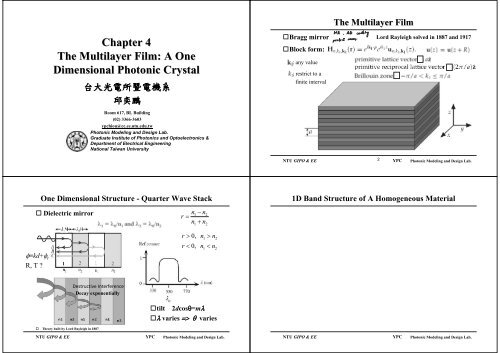
Chapter 4<br />
The Multilayer Film: A <strong>One</strong><br />
<strong>Dimensional</strong> <strong>Photonic</strong> <strong>Crystal</strong><br />
台大光電所暨電機系<br />
邱奕鵬<br />
Room 617, BL Building<br />
(02) 3366-3603<br />
ypchiou@cc.ee.ntu.edu.tw<br />
<strong>Photonic</strong> Modeling and Design Lab.<br />
Graduate Institute of <strong>Photonic</strong>s and Optoelectronics &<br />
Department of Electrical Engineering<br />
National Taiwan University<br />
<strong>One</strong> <strong>Dimensional</strong> Structure - Quarter Wave Stack<br />
n − n<br />
r =<br />
n + n<br />
Dielectric mirror 1 2<br />
φ=kd+φ r<br />
R, T ?<br />
Destructive Interference<br />
Decay exponentially<br />
Theory built by Lord Rayleigh in 1887<br />
1 2<br />
r > 0, n > n<br />
r < 0, n < n<br />
1 2<br />
1 2<br />
tilt 2dcosθ=mλ<br />
λ varies => θ varies<br />
NTU GIPO & EE YPC <strong>Photonic</strong> Modeling and Design Lab.<br />
Block form:<br />
The Multilayer Film<br />
Bragg mirror Lord Rayleigh solved in 1887 and 1917<br />
: any value<br />
: restrict to a<br />
finite interval<br />
NTU GIPO & EE 2 YPC <strong>Photonic</strong> Modeling and Design Lab.<br />
1D Band Structure of A Homogeneous Material<br />
NTU GIPO & EE YPC <strong>Photonic</strong> Modeling and Design Lab.
Helmholtz eq.<br />
∂ ψ ω<br />
∂z<br />
c<br />
ω<br />
ψ1 = A1cosαx+ B1sinαx α = n1<br />
c<br />
ω<br />
ψ = A cos βx+ B sin βx β = n<br />
c<br />
2 2 2 2<br />
z = 0<br />
A1 = A2<br />
B1α= B2β<br />
'<br />
ψ1 =− A1αsinα0+ B1αcosα0<br />
'<br />
ψ =− A β sin β0+ B β cos β0<br />
2 2 2<br />
Kronig Penney Model<br />
2 2<br />
2 +<br />
2<br />
n ψ = 0<br />
2<br />
z = p (Bloch thm.)<br />
ika<br />
ψ1( x + a) = e ψ1(<br />
x)<br />
ika<br />
ψ1( p) = ψ1( − q+ a) = e ψ1(<br />
−q)<br />
' ika '<br />
ψ ( p) = e ψ ( −q)<br />
1 1<br />
⎧⎪ ψ1 = ψ 2<br />
B.C. ⎨ ' '<br />
⎪⎩ ψ1 = ψ 2<br />
across interfaces<br />
period a = p+q<br />
⎡ ika ika α ⎤<br />
⎢ e cosαq−cos β p −e sinαq− sin β p A1<br />
β ⎥⎡<br />
⎤<br />
= 0<br />
⎢ ⎥⎢ ika ika<br />
B<br />
⎥<br />
1<br />
⎢e αsinαq+ βsin β p e αcosαq−αcos β p⎥<br />
⎣ ⎦<br />
⎣ ⎦<br />
1 2<br />
det ( M ) = 0<br />
HW#2.3<br />
2 2<br />
α + β<br />
cos ka =− sinαqsinβ p + cosαqcos β p<br />
2αβ<br />
2 2<br />
n1 + n2<br />
⎛ω ⎞ ⎛ω ⎞ ⎛ ω ⎞ ⎛ ω ⎞<br />
=− sin nq 1 sin n2pcosn1 q cos n2 p<br />
2nn<br />
⎜<br />
c<br />
⎟ ⎜ +<br />
c<br />
⎟ ⎜<br />
c<br />
⎟ ⎜<br />
c<br />
⎟<br />
⎝ ⎠ ⎝ ⎠ ⎝ ⎠ ⎝ ⎠<br />
NTU GIPO & EE 5 YPC <strong>Photonic</strong> Modeling and Design Lab.<br />
The Physical Origin of <strong>Photonic</strong> Band Gaps<br />
Nearly Nearly-homogeneous homogeneous medium<br />
Smaller index difference<br />
⇒Narrow-band filter, e.g. in opt. comm.<br />
fiber Bragg grating, thin-film filter<br />
Wavelength<br />
3(a) or 3(b), otherwise<br />
violate symmetry<br />
More field in high-ε<br />
=> lower freq.<br />
more field in low-ε<br />
=> higher freq.<br />
air band<br />
dielectric band<br />
NTU GIPO & EE 7 YPC <strong>Photonic</strong> Modeling and Design Lab.<br />
The Physical Origin of <strong>Photonic</strong> Band Gaps<br />
<strong>Photonic</strong> band gap: no allowed mode regardless of k<br />
Light lines<br />
ε= 13 & 13 ε= 13 (GaAs) & 12 (AlGaAs) ε= 13 & 1<br />
NTU GIPO & EE 6 YPC <strong>Photonic</strong> Modeling and Design Lab.<br />
Simple Plane Wave Expansion Approach (1D)<br />
Helmholtz Equation<br />
2 2 2<br />
c ∂ E ∂ E 1D<br />
ε<br />
=<br />
←⎯⎯<br />
2<br />
1<br />
∂ E<br />
∇×<br />
∇×<br />
E = −<br />
2 2<br />
2<br />
( x)<br />
∂x<br />
∂t<br />
ε ( r ) ∂t<br />
( x a)<br />
ε(<br />
x)<br />
+ ( ) ∑ ∞<br />
−1<br />
ε x =<br />
m=<br />
−∞<br />
ε =<br />
ε : lossless → ε<br />
κ<br />
−m<br />
= κ<br />
*<br />
m<br />
κ<br />
κ<br />
is real<br />
−1<br />
→ κ ∝ ε<br />
m<br />
−m<br />
*<br />
m<br />
∝<br />
∝<br />
∫<br />
( x)<br />
e<br />
2π<br />
−i<br />
mx<br />
a<br />
2π<br />
κ me<br />
dx<br />
i mx<br />
−1<br />
a<br />
∫ε<br />
( x)<br />
e dx<br />
2π<br />
i mx<br />
−1<br />
*<br />
a<br />
∫ [ ε ( x)<br />
] e dx<br />
From Bloch theorem<br />
ikx −i<br />
t<br />
E(<br />
x,<br />
t)<br />
= E ( x,<br />
t)<br />
= e u ( x)<br />
e = u ( x)<br />
k<br />
u<br />
k<br />
( x)<br />
∑<br />
= m<br />
E<br />
k<br />
2π<br />
i mx<br />
a<br />
me<br />
2π<br />
i mx<br />
a<br />
( ) t kx i<br />
ωk −ωk<br />
k e<br />
( x,<br />
t)<br />
NTU GIPO & EE YPC <strong>Photonic</strong> Modeling and Design Lab.<br />
E<br />
k<br />
−<br />
ε<br />
=<br />
=<br />
( x)<br />
1<br />
∑<br />
m<br />
∑<br />
m<br />
E<br />
E<br />
2π<br />
i mx<br />
a ikx −iωt<br />
me<br />
e e<br />
⎛ 2π<br />
⎞<br />
i⎜<br />
k + m ⎟ x−iωt<br />
⎝ a ⎠<br />
me<br />
small ε difference or<br />
sinusoidal distribution<br />
∞ 2π<br />
i mx<br />
a κ me<br />
m=<br />
−∞<br />
= ∑<br />
≅ κ + κ<br />
0<br />
2π<br />
i x<br />
a<br />
1e<br />
(Cf. 1D Equations)<br />
+ κ<br />
2π<br />
−i<br />
x<br />
a<br />
−1e<br />
π<br />
h≡k− a<br />
πc<br />
ac ⎛ ⎞<br />
ω± = κ ± κ ± κ −<br />
a<br />
⎝ ⎠<br />
2<br />
2 κ1<br />
2<br />
0 1 ⎜ 0 ⎟h<br />
πκ ⎜ 1 2 ⎟
The Physical Origin of <strong>Photonic</strong> Band Gaps<br />
Higher Higher dielectric contrast<br />
1ST band are more concentrated than<br />
2nd band in high–ε region<br />
Gap occurs at center<br />
or edge of Brillouin<br />
zone<br />
Gaps always appear<br />
in 1D PhC as<br />
air band<br />
dielectric band<br />
NTU GIPO & EE 9 YPC <strong>Photonic</strong> Modeling and Design Lab.<br />
Gap max. as<br />
Quarter-wave stack (QWS)<br />
Reflective waves from each<br />
layer is exactly in phase.<br />
HW#3<br />
Dielectric contrast 13:1<br />
d1:d2 =0.5: 0.5 => Δω/ωm =51.9%<br />
d1=0.217=> Δω/ωm =76.6% (QWS)<br />
d1:d2 =0.2: 0.8 => Δω/ωm =76.3%<br />
QWS => no gap @ k=0 HW#3<br />
The Size of the Band Gap<br />
HW#3<br />
HW#3<br />
(ε1=13, d1=0.2a, ε2=1, d2=08a)<br />
NTU GIPO & EE 11 YPC <strong>Photonic</strong> Modeling and Design Lab.<br />
The Size of the Band Gap<br />
Scaling property<br />
Structure expanded by a factor s => gap size Δω/s<br />
Gap-midgap ratio Δω/ωm, ωm: freq. at the middle of the gap, generally in %<br />
Normalized (dimensionless)<br />
wavevector: ka/2π , freq. ωa/2πc = a/λ<br />
Weak periodicity Δε/ ε
No band gaps ( no scattering in y)<br />
No degeneracy (split: TMy & TEy )<br />
Approximately linear at<br />
long wavelengths<br />
for all PhC<br />
effectively homogeneous<br />
lower modes concentrate<br />
electrical energy in the<br />
higher ε-region<br />
ω TM < ω TE<br />
Off-Axis Off Axis Propagation<br />
NTU GIPO & EE 13 YPC <strong>Photonic</strong> Modeling and Design Lab.<br />
Localized Modes at Defects<br />
Defects + ω in band gap<br />
may exist localized modes<br />
0.2 a (ε=13) + 0.8a (ε=1)<br />
Like two parallel perfect mirrors<br />
discrete freq. (quantized)<br />
thicker defect => more states<br />
1.6a =<br />
2*0.8a<br />
E-field strength<br />
Quantized like particle in a box (QM) or metallic cavity (μ-wave)<br />
Defects by<br />
Increase low/high-ε thickness<br />
or lower/increase ε (same thick.)<br />
or combined<br />
Pull down/push up a sequence<br />
of discrete modes from the<br />
upper/lower bands<br />
Max. exp. decay in mid-gap<br />
Single peak associate with the defect<br />
Used in dielectric Fabry-Perot filter<br />
DOS<br />
= # states / Δω<br />
NTU GIPO & EE 15 YPC <strong>Photonic</strong> Modeling and Design Lab.<br />
Short wavelength (high freq.)<br />
Freq. difference<br />
Below light line<br />
* index guided<br />
* decay exp.<br />
* negligible overlap<br />
* small coupling<br />
Every mode become<br />
a uncoupled<br />
guided mode<br />
Off-Axis Off Axis Propagation<br />
Blue: (0, k y,0)<br />
Green: (0, k y, π/a)<br />
Red: light line<br />
NTU GIPO & EE 14 YPC <strong>Photonic</strong> Modeling and Design Lab.<br />
Localized Modes at Defects<br />
Defects by<br />
Increase low/high-ε thickness<br />
or lower/increase ε (same thick.)<br />
or combined<br />
Pull down/push up a sequence<br />
of discrete modes from the<br />
upper/lower bands<br />
Off-axis propagation<br />
Still localized in z-direction<br />
Can be guided in both<br />
High and low ε regions (even air)<br />
2D => photonic crystal fibers (PCF)<br />
NTU GIPO & EE 16 YPC <strong>Photonic</strong> Modeling and Design Lab.
May exist localized modes<br />
propagating along surface<br />
(e.g. And x-polarized )<br />
Extended (E): propagating<br />
Decaying (D): evanescent<br />
Air region: light line<br />
upper left =><br />
lower right=><br />
PhC region:<br />
w/ gap:<br />
w/o gap:<br />
Surface modes for some choice<br />
of termination (e.g. 0.1 a)<br />
Surface states<br />
0.1 a<br />
air + dielectric<br />
NTU GIPO & EE 17 YPC <strong>Photonic</strong> Modeling and Design Lab.<br />
Optimal: not quarter wave<br />
stacks but close to<br />
Reflective property dep. on<br />
translational symmetry<br />
=> Not confine a mode in 3D<br />
If the interface is not flat or<br />
an object close to,<br />
then is not conserved.<br />
=> couple to extended modes<br />
i.e. propagating<br />
transmitted<br />
Exceptions: smoothly curved<br />
and symmetry conserved<br />
Continuous rotational and<br />
spherical symmetry<br />
Omnidirectional Multilayer Mirrors<br />
Size of the omnidirectional gap<br />
ε a < ε 1 < ε 2<br />
NTU GIPO & EE 19 YPC <strong>Photonic</strong> Modeling and Design Lab.<br />
Omnidirectional Multilayer Mirrors<br />
Can reflect light wave from any<br />
angle with any polarization<br />
is conserved (far source)<br />
from air<br />
(above light line, not decay<br />
light from source can reach)<br />
Necessary conditions<br />
ω U > ω L<br />
large enough to open<br />
gap within light cone<br />
ε a < ε 1 < ε 2<br />
point B below light line<br />
ky = kasinθ a = k1sinθ1 = k2sinθ2<br />
nasinθa = n1sinθ1 = n2sinθ2<br />
n1<br />
tanθ<br />
B =<br />
n<br />
a<br />
ambient ε a<br />
Brewster’s angle line<br />
TE, yz-polarized<br />
TM, x-polarized<br />
a quarter-wave stack with ε = 13 & 2<br />
NTU GIPO & EE 18 YPC <strong>Photonic</strong> Modeling and Design Lab.<br />
Omnidirectional Multilayer Mirrors<br />
Translational Symmetry<br />
⇒Cylindrical & Spherical cases<br />
Continuous rotational and<br />
spherical symmetry<br />
Brag fiber<br />
Brag onion<br />
OL 28, 2144 (2003)<br />
(See Chap. 9 PCF)<br />
NTU GIPO & EE 20 YPC <strong>Photonic</strong> Modeling and Design Lab.
Periodic Hermitian Eigenproblems in 1d<br />
H(x) = e ikx H k (x)<br />
Consider k+2π/a: e<br />
ε 1 ε 2 ε 1 ε 2 ε 1 ε 2 ε 1 ε 2 ε 1 ε 2 ε 1 ε 2<br />
a<br />
2π<br />
i(k + ) x<br />
a H 2π<br />
k +<br />
a<br />
k is periodic:<br />
k + 2π/a equivalent to k<br />
“quasi-phase-matching”<br />
ε(x) = ε(x+a)<br />
(x) = e ikx ⎡<br />
⎢ e<br />
⎣ ⎢<br />
2π<br />
i<br />
a x<br />
H 2π<br />
k +<br />
a<br />
⎤<br />
(x) ⎥<br />
⎦ ⎥<br />
periodic!<br />
satisfies same<br />
equation as H k<br />
= H k<br />
NTU GIPO & EE YPC <strong>Photonic</strong> Modeling and Design Lab.<br />
Any 1d Periodic System has a Gap<br />
[ Lord Rayleigh, “On the maintenance of vibrations by forces of double frequency, and on the propagation of<br />
waves through a medium endowed with a periodic structure,” Philosophical Magazine 24, 145–159 (1887). ]<br />
Start with<br />
a uniform (1d) medium:<br />
ω<br />
0<br />
NTU GIPO & EE YPC <strong>Photonic</strong> Modeling and Design Lab.<br />
ε 1<br />
ω = k<br />
ε 1<br />
k<br />
Periodic Hermitian Eigenproblems in 1d<br />
k is periodic:<br />
k + 2π/a equivalent to k<br />
“quasi-phase-matching”<br />
–π/a<br />
ω<br />
ε 1 ε 2 ε 1 ε 2 ε 1 ε 2 ε 1 ε 2 ε 1 ε 2 ε 1 ε 2<br />
band gap<br />
ε(x) = ε(x+a)<br />
NTU GIPO & EE YPC <strong>Photonic</strong> Modeling and Design Lab.<br />
a<br />
0 π/a<br />
irreducible Brillouin zone<br />
Any 1d Periodic System has a Gap<br />
[ Lord Rayleigh, “On the maintenance of vibrations by forces of double frequency, and on the propagation of<br />
waves through a medium endowed with a periodic structure,” Philosophical Magazine 24, 145–159 (1887). ]<br />
Treat it as<br />
“artificially” periodic<br />
bands are “folded”<br />
by 2π/a equivalence<br />
–π/a<br />
ω<br />
NTU GIPO & EE YPC <strong>Photonic</strong> Modeling and Design Lab.<br />
a<br />
ε 1<br />
ε(x) = ε(x+a)<br />
k<br />
π<br />
+<br />
a e x<br />
π<br />
−<br />
a , e x<br />
→ cos<br />
0 π/a<br />
k<br />
π<br />
a x<br />
⎛ ⎞<br />
⎜ ⎟ , sin<br />
⎝ ⎠<br />
π<br />
a x<br />
⎛ ⎞<br />
⎜<br />
⎝ ⎠
ω<br />
Any 1d Periodic System has a Gap<br />
[ Lord Rayleigh, “On the maintenance of vibrations by forces of double frequency, and on the propagation of<br />
waves through a medium endowed with a periodic structure,” Philosophical Magazine 24, 145–159 (1887). ]<br />
Treat it as<br />
“artificially” periodic<br />
0 π/a<br />
ω<br />
sin π<br />
a x<br />
⎛ ⎞<br />
⎜ ⎟<br />
⎝ ⎠<br />
cos π<br />
a x<br />
⎛ ⎞<br />
⎜ ⎟<br />
⎝ ⎠<br />
ε 1<br />
ε(x) = ε(x+a)<br />
NTU GIPO & EE YPC <strong>Photonic</strong> Modeling and Design Lab.<br />
band gap<br />
a<br />
x = 0<br />
Any 1d Periodic System has a Gap<br />
[ Lord Rayleigh, “On the maintenance of vibrations by forces of double frequency, and on the propagation of<br />
waves through a medium endowed with a periodic structure,” Philosophical Magazine 24, 145–159 (1887). ]<br />
Add a small<br />
“real” periodicity<br />
ε 2 = ε 1 + Δε<br />
0 π/a<br />
sin π<br />
a x<br />
⎛ ⎞<br />
⎜ ⎟<br />
⎝ ⎠<br />
cos π<br />
a x<br />
⎛ ⎞<br />
⎜ ⎟<br />
⎝ ⎠<br />
Splitting of degeneracy:<br />
state concentrated in higher index (ε 2)<br />
has lower frequency<br />
NTU GIPO & EE YPC <strong>Photonic</strong> Modeling and Design Lab.<br />
a<br />
ε(x) = ε(x+a)<br />
ε 1 ε 2 ε 1 ε 2 ε 1 ε 2 ε 1 ε 2 ε 1 ε 2 ε 1 ε 2<br />
x = 0<br />
ω<br />
Any 1d Periodic System has a Gap<br />
[ Lord Rayleigh, “On the maintenance of vibrations by forces of double frequency, and on the propagation of<br />
waves through a medium endowed with a periodic structure,” Philosophical Magazine 24, 145–159 (1887). ]<br />
Add a small<br />
“real” periodicity<br />
ε 2 = ε 1 + Δε<br />
0 π/a<br />
sin π<br />
a x<br />
⎛ ⎞<br />
⎜ ⎟<br />
⎝ ⎠<br />
cos π<br />
a x<br />
⎛ ⎞<br />
⎜ ⎟<br />
⎝ ⎠<br />
ε(x) = ε(x+a)<br />
NTU GIPO & EE YPC <strong>Photonic</strong> Modeling and Design Lab.<br />
a<br />
ε 1 ε 2 ε 1 ε 2 ε 1 ε 2 ε 1 ε 2 ε 1 ε 2 ε 1 ε 2<br />
x = 0