two-Channel PC- baSed oSCilloSCoPe - Kits 'n' Spares
two-Channel PC- baSed oSCilloSCoPe - Kits 'n' Spares
two-Channel PC- baSed oSCilloSCoPe - Kits 'n' Spares

Create successful ePaper yourself
Turn your PDF publications into a flip-book with our unique Google optimized e-Paper software.
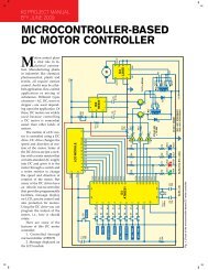
ConstruCtion<br />
<strong>two</strong>-<strong>Channel</strong> <strong>PC</strong><strong>baSed</strong><br />
<strong>oSCilloSCoPe</strong><br />
Gerard SamblanCat<br />
More and more experiments<br />
are now ‘<strong>PC</strong>-assisted.’ Also<br />
conventional acquisition systems<br />
are very expensive. Since portable<br />
<strong>PC</strong>s are today common and a USB link<br />
is a better solution than an old ISA bus,<br />
Author’s prototype<br />
here we present an oscilloscope using<br />
USB port of the <strong>PC</strong> that operates at up<br />
to 10 kHz with ±16V input voltage. It<br />
has much more improved features than<br />
the <strong>PC</strong>-based oscilloscope and LED<br />
scope for audio servicing published in<br />
EFY Dec. 2002 and Electronics Projects<br />
Vol. 8, respectively. The oscilloscope<br />
uses IC PIC18F2550 from Microchip<br />
as the main controller, which makes<br />
the oscilloscope compact as there is no<br />
need of additional power supply for<br />
the entire circuit board. The prototype<br />
of the circuit along with the enclosure<br />
is shown above.<br />
Circuit description<br />
At the heart of this oscilloscope is<br />
USB2.0-compliant microcontroller<br />
PIC18F2550 from Microchip. You<br />
can also use PIC18F2445 in place of<br />
PIC18F2550. Specifications of this mi-<br />
crocontroller are given here in the box.<br />
This microcontroller has a USB2.0-compliant<br />
transceiver and a CPU running<br />
up to 12 MIPS.<br />
Fig. 1 shows the circuit of the<br />
<strong>two</strong>-channel <strong>PC</strong>-based oscilloscope.<br />
MCP6S91 from Microchip Technology<br />
is an analogue programmable gain amplifier<br />
that is well suited<br />
to driving analogue-todigital<br />
converters (ADCs)<br />
and an analogue input to<br />
a PIC microcontroller.<br />
Two MCP6S91 programmable<br />
gain amplifiers<br />
(IC2 and IC3) make<br />
it possible to choose the<br />
input ranges for each of<br />
the <strong>two</strong> channels, by selecting<br />
a gain from 1:1 to<br />
32:1. The amplifiers are<br />
small, cheap and easy to<br />
use. A simple three-wire<br />
serial peripheral interface<br />
(SPI) allows the PIC<br />
to control them through<br />
Features of PIC18F2550<br />
Programming<br />
1. Up to 32 kB of flash memory, 2kB RAM and 256-byte EEPROM<br />
2. Extended instruction set (optimised for ‘C’ compiler)<br />
3. 8x8 single-cycle multiplier<br />
4. Single-supply serial programming and easy debugging<br />
USB transceiver<br />
1. USB1.1 and 2.0 from 1.5 MB/s to 12 MB/s<br />
2. Isochronous, bulk and interrupt transfer modes<br />
3. 1 kB of access RAM usable with 32 endpoints (64 bytes each)<br />
Multiple oscillator and power modes<br />
1. From internal 31 kHz to external 48 MHz with PLL<br />
2. Possible software switching between ‘run,’ ‘idle’ and sleep<br />
modes. In sleep mode, current is down to 0.1 µA.<br />
3. Wide operating voltage range (2.0V to 5.5V). Useful for battery<br />
operations.<br />
Complete set of classical peripherals<br />
1. Several input/output (I/O) ports, four timers with capture/<br />
compares<br />
2. Synchronous and asynchronous enhanced modules<br />
3. Streaming parallel port<br />
4. 10-bit ADC module with up to 13-channel multiplexer.<br />
its pins 5, 6 and 7.<br />
The MCP6S91 amplifier is designed<br />
with CMOS input devices. It is designed<br />
to not exhibit phase inversion<br />
when the input pins exceed the supply<br />
voltages. The maximum voltage that<br />
can be applied to the input pin is –0.3V<br />
(V SS ) to +0.3V (V DD ). Input voltages that<br />
exceed this absolute maximum rating<br />
can cause excessive current into or out<br />
of the input pins. Current beyond ±2<br />
mA can cause reliability problems. Applications<br />
that exceed this rating must<br />
be externally limited with a resistor to<br />
the input pin.<br />
Vref (pin 3), which is an analogue<br />
input, should be at a voltage between<br />
V SS and V DD . The voltage at this pin<br />
shifts the output voltage. The SPI<br />
interface inputs are chip-select (CS),<br />
serial input (SI) and serial clock (SCK).<br />
These are Schmitt-triggered, CMOS<br />
logic inputs.<br />
The only disadvantage is that these<br />
amplifiers accept only positive signals.<br />
That’s why voltage-shifting amplifiers<br />
LF353 (IC4A<br />
and IC5A) are used,<br />
one each for each<br />
channel input (see<br />
Fig. 1). The LF353<br />
is a JFET input operational<br />
amplifier<br />
with an internally<br />
compensated input<br />
offset voltage. The<br />
JFET input device<br />
provides wide bandwidth,<br />
low input<br />
bias currents and<br />
offset currents. This<br />
voltage-shifting amplifier<br />
results in a<br />
high input impedance<br />
and an attenuation<br />
factor of 1:4.5.<br />
A ±16V input signal<br />
is then shifted to the<br />
60 • D e c e m b e r 2 006 • electronics for you w w w . e f y m a g . c o m
0-5V range when the programmed<br />
gain is 1:1.<br />
Two halves of the<br />
LF353 (IC4B and IC5B) are<br />
used as voltage followers<br />
to provide a low-impedance<br />
shifting voltage<br />
(Vref) to the programmable<br />
amplifiers. This<br />
voltage must be precisely<br />
adjusted with <strong>two</strong> 4.7-kiloohm<br />
presets to measure<br />
precisely 2.5V level on<br />
the inputs of IC2 and IC3<br />
when the input signals are<br />
grounded.<br />
Because LF353 opamps<br />
need a symmetrical<br />
supply voltage, a small<br />
DC-DC voltage converter<br />
ICL7660 (IC6) is used<br />
to feed –5V to LF353.<br />
With its small 8-pin DIP<br />
package, it needs only<br />
<strong>two</strong> polarised capacitors.<br />
ICL7660 can be replaced<br />
with a MAX1044. The<br />
MAX1044 and ICL7660<br />
are monolithic, CMOS<br />
switched-capacitor voltage<br />
converters that invert,<br />
double, divide or multiply<br />
a positive input voltage.<br />
These are pin compatible<br />
with the industry-standard<br />
LTC1044.<br />
overview of the<br />
universal serial<br />
bus<br />
w w w . e f y m a g . c o m<br />
Fig. 1: Two-channel <strong>PC</strong>-based oscilloscope circuit<br />
The specifications of the<br />
USB can be found on website<br />
‘www.usb.org.’ One<br />
of its major advantages<br />
is the ability to drive 5V,<br />
100mA devices.<br />
All the data is transmitted<br />
on the D+/D- symmetrical<br />
pins using a variable<br />
bit rate. The position<br />
of a resistor (R13) on D+<br />
or D- allows you to choose between<br />
the full-speed (12 Mbps) and lowspeed<br />
modes (1.5 Mbps). Note that the<br />
PIC18F2550/2455 devices have built-in<br />
pull-up resistors designed to meet the<br />
requirements of low-speed and full-<br />
speed USB. The UPUEN bit (UCFG=4)<br />
enables the internal pull-ups. In this<br />
project, R13 is not used. External pullup<br />
may also be used. The VUSB pin<br />
may be used to pull up D+ or D-. The<br />
pull-up resistor must be 1.5 kilo-ohms<br />
(±5%) as required by the USB specifica-<br />
ConstruCtion<br />
tions.<br />
You can also ‘hot-plug’ a new device.<br />
When this is done, the host <strong>PC</strong><br />
starts an enumeration process to identify<br />
the device. The device sends the information<br />
to the <strong>PC</strong> by way of different<br />
‘descriptors.’ Each descriptor contains<br />
electronics for you • D e c e m b e r 2006 • 61
ConstruCtion<br />
Fig. 2: Layered framework of a USB device<br />
a specific kind of information about<br />
the device (vendor ID, serial number,<br />
format and type of data transmitted).<br />
You can see in Fig. 2 that each<br />
device is structured in a layered framework<br />
of descriptors. The first layer containing<br />
the configuration descriptors<br />
describes the power mode.<br />
Each configuration may have different<br />
interfaces and each interface<br />
may have different endpoints. An<br />
interface can use several endpoints<br />
and an endpoint can be ‘IN’ (data from<br />
device to the host) or ‘OUT’ (from host<br />
to the device). With such an opened<br />
structure, it’s important to carefully<br />
design the descriptors.<br />
A 64-byte buffer is allocated to<br />
each of the 32 possible endpoints. Here<br />
only one is used and the more possible<br />
amount of RAM buffer is then reallocated<br />
to store the measured values.<br />
the PiC software<br />
The program for the microcontroller<br />
is written in ‘C’ language. MPLAB<br />
7.31 along with MPLAB_C18 is used<br />
as the software tool for development.<br />
The software tools can be<br />
downloaded for free from website<br />
‘www.microchip.com.’<br />
Based on Microchip’s application<br />
notes, the program for the chip is centered<br />
on a main loop continually polling<br />
the USB transceiver state. This loop<br />
never stops and each USB operation is<br />
done in one pass. All operations are<br />
initiated by the host (the <strong>PC</strong>), which<br />
sends a 16-byte command.<br />
The first command byte determines<br />
the chip actions. The four possible actions<br />
are:<br />
1. Command 80h: Clears the EE-<br />
PROM calibration memory<br />
2. Command 81h: Receives parameters,<br />
and stores the gain-error compensation<br />
for the <strong>two</strong> channels.<br />
3. Command 83h: Initiates a zero<br />
calibration sequence of the <strong>two</strong> chan-<br />
Parts List<br />
Semiconductors:<br />
IC1 - PIC18F2550 microcontroller<br />
IC2, IC3 - MCP6S91 programmable<br />
gain amplifier<br />
IC4(A, B),<br />
IC5(A, B) - LF353 dual operational<br />
amplifier<br />
IC6 - ICL7660 switched-capacitor<br />
voltage converters<br />
Resistors (all ¼-watt, ±5% carbon):<br />
R1, R7 - 1-mega-ohm<br />
R2, R8 - 82-kilo-ohm<br />
R3, R9 - 33-kilo-ohm<br />
R4, R10 - 220-kilo-ohm<br />
R5, R11 - 150-kilo-ohm<br />
R6, R12 - 1-kilo-ohm<br />
Capacitors:<br />
C1, C2 - 2.7pF ceramic<br />
C3, C4,<br />
C5, C6 - 68nF ceramic<br />
C7 - 0.022µF polyester<br />
C8 - 150nF ceramic<br />
C9 - 10µF, 16V electrolytic<br />
C10 - 47µF, 16V electrolytic<br />
Miscellaneous:<br />
X1 - 4MHz crystal oscillator<br />
CON1 - USB socket (type-B) for<br />
<strong>PC</strong>B<br />
nels. The <strong>two</strong> inputs have to be<br />
grounded.<br />
4. Command 85h: Initiates measurement<br />
of the input signals.<br />
The PIC software consists of<br />
eight ‘C’ program source files, 14<br />
header files and a linker file all under<br />
‘aquis.mcp’ project. The main<br />
‘C’ program source files (‘main.c’<br />
and ‘user.c’) are given at the end of<br />
this article. The rest of the program<br />
files are included in the EFY-CD.<br />
Programming the chip. Programming<br />
the PIC18F2455/2550 is easy<br />
with an ICD2 module or PICSTART<br />
Plus development board along with<br />
MPLAB software. But many serial<br />
programmers for PIC16F84 are not<br />
compatible here. While using the<br />
PICSTART Plus development board,<br />
you can copy the hex file into the<br />
MPLAB IDE using ‘import’ command<br />
from ‘file’ menu bar. Select the device<br />
as ‘PIC18F2550’ and configure the bits<br />
as per this device from ‘config’ menu.<br />
Installation of the USB driver. 1. If<br />
everything is fine, plug the oscilloscope<br />
with a USB cable to your <strong>PC</strong> (running<br />
Windows 98SE or higher version). A<br />
“new hardware detected–USB2-MiniOscilloscope”<br />
dialogue box must immediately<br />
appear on the screen.<br />
2. Now you can start the driver installation<br />
process. The driver has been<br />
included in the EFY-CD. The goal is<br />
to select a good driver (mchpusb.inf)<br />
by choosing the ‘specific location’ option.<br />
Don’t let Windows take a generic<br />
driver by default.<br />
3. When you are done with<br />
installation, go to ‘device manager’<br />
and check whether ‘USB2-MiniOscilloscope’<br />
is under ‘other device’ in ‘view<br />
devices by type’ option. Otherwise,<br />
repeat Steps 1 and 2.<br />
User interface program and operations.<br />
A user-interface software<br />
written in Visual Basic 6, called ‘OscilloPIC,’<br />
is included in the EFY-CD.<br />
Run the set up program from the<br />
‘Setup_files’ folder included in the<br />
EFY-CD. This will automatically install<br />
the ‘OscilloPIC’ user-interface program.<br />
Alternatively, you can open the<br />
‘Source_VB6’ folder, compile and run<br />
the ‘Synchropic’ program using Visual<br />
Basic 6. Now run the ‘OscilloPIC.’ The<br />
62 • D e c e m b e r 2 006 • electronics for you w w w . e f y m a g . c o m
application program looks like a<br />
small digital oscilloscope as shown<br />
in the screenshot below.<br />
Various settings for operations<br />
are given in the following menu<br />
bars:<br />
1. Inputs: Selects the active<br />
channels<br />
2. Sampling: Sets time-base and<br />
number of samples<br />
3. Trigger: Sets the triggering<br />
condition<br />
4. Cursors: Selects horizontal or<br />
vertical cursor positions<br />
5. Num: Shows numerical<br />
sampled values, with an export<br />
command (text file format)<br />
6. Config: Configures gain and<br />
offset errors<br />
Calibration is to be done as<br />
described below before reading<br />
the output signals on the monitor<br />
screen by clicking ‘channels calibration’<br />
under ‘config’ menu bar.<br />
Feed the input waveforms (say,<br />
sine, rectangular, sawtooth, etc)<br />
from the source. Click ‘go’ button.<br />
The output waveform will be<br />
displayed on the monitor screen.<br />
<strong>Channel</strong>-1 and channel-2 output<br />
waveforms can be differentiated by<br />
green and red lines, respectively.<br />
By default, the time base is 200 µs<br />
per division and amplitude is 4V<br />
per division. You can set these parameters<br />
as per your requirements.<br />
Test and calibration. The first<br />
step is to adjust the zero offset error.<br />
Connect the <strong>two</strong> analogue inputs to<br />
the ground level and tune the <strong>two</strong> 4.7-<br />
Screenshot: Oscilloscopic program output screen along with typical<br />
sine and triangular waveforms<br />
w w w . e f y m a g . c o m<br />
kilo-ohm presets until pin 2 of both<br />
MCP6S21 is at 2.5V. A more precise<br />
tuning can be achieved through ‘OscilloPIC’<br />
software. Choose the smallest<br />
calibration value at ±0.5V for both the<br />
inputs.<br />
The ‘zero calibration’<br />
command tells the PIC<br />
to start its own internal<br />
compensation for all calibrations.<br />
Don’t forget to<br />
connect the inputs to the<br />
ground while calibrating.<br />
The second parameter<br />
to check is the gain error.<br />
By clicking the ‘gain calibration’<br />
command, it’s<br />
possible to specify a small<br />
correction factor. This<br />
can be done after several<br />
measurements. You have<br />
to know the actual levels<br />
ConstruCtion<br />
Fig. 3: An actual-size, single-side <strong>PC</strong>B layout of the <strong>two</strong>-channel <strong>PC</strong>-based USB oscilloscope<br />
Fig. 4: Component layout for the <strong>PC</strong>B<br />
and the measured levels (with the cursors)<br />
for the <strong>two</strong> channels. The gain error<br />
is less than 0.1 per cent. The number<br />
of samples can be set between ‘10’ and<br />
‘500.’ The minimum sampling rate is<br />
5 µs for one channel and 10 µs for <strong>two</strong><br />
channels.<br />
Construction<br />
An actual-size, single-side <strong>PC</strong>B layout<br />
for the <strong>two</strong>-channel <strong>PC</strong>-based USB oscilloscope<br />
circuit is shown in Fig. 3 and<br />
its component layout in Fig. 4. Since<br />
the circuit is compact, the construction<br />
is easy. It is advised to use IC bases for<br />
mounting IC2 through IC6 on the <strong>PC</strong>B<br />
for easy troubleshooting. The USB connector<br />
(CON1) must be firmly soldered<br />
and fixed on the board. It is located on<br />
the extreme right of the board (refer<br />
Fig. 4).<br />
Two BNC connectors can be used<br />
for the input signals for channels ‘1’<br />
electronics for you • D e c e m b e r 2006 • 63
ConstruCtion<br />
and ‘2,’ respectively. The connectors<br />
can be fixed on the front panel of the<br />
enclosure.<br />
The performance of the oscilloscope<br />
can be improved by changing the PIC<br />
and its ADC with a faster model.<br />
/**********************************************************<br />
* FileName: main.c<br />
* Dependencies: See INCLUDES section below<br />
/** I N C L U D E S ************************************/<br />
#include “p18f2550.h”<br />
#include “typedefs.h” // Required<br />
#include “usb.h” // Required<br />
#include “io_cfg.h” // Required<br />
#include “user.h” // Modifiable<br />
/** V A R I A B L E S ***********************************/<br />
#pragma udata<br />
extern unsigned char voie1[256];<br />
extern unsigned char voie2[256];<br />
extern unsigned char voiesH1[64],voiesH2[64];<br />
extern char ordre, timeout;<br />
/** P R I V A T E P R O T O T Y P E S ****************/<br />
static void InitializeSystem(void);<br />
void USBTasks(void);<br />
void timer_isr(void);<br />
/** V E C T O R M A P P I N G *********************/<br />
extern void _startup (void); // See c018i.c in<br />
//your C18 compiler dir<br />
#pragma code _RESET_INTERRUPT_VECTOR =<br />
0x000800<br />
void _reset (void) {<br />
_asm goto _startup<br />
_endasm<br />
}<br />
#pragma code<br />
#pragma code low_vector = 0x18<br />
void low_interrupt (void) {<br />
_asm goto timer_isr _endasm<br />
}<br />
#pragma code<br />
#pragma interruptlow timer_isr<br />
//Fixe une periode de 1 seconde pour le time-out<br />
//aquisition<br />
/**********************************************************<br />
* FileName: user.c<br />
* Processor: PIC18<br />
********************************************************<br />
************/<br />
/** I N C L U D E S ************************************/<br />
#include “p18f2550.h”<br />
#include “typedefs.h”<br />
#include “usb.h”<br />
#include “io_cfg.h” // I/O pin mapping<br />
#include “user.h”<br />
/** V A R I A B L E S **********************************/<br />
#pragma udata<br />
DATA_PACKET databuff;<br />
//Caracteristiques de l’acquisition<br />
unsigned char t_basethh, t_baseth, t_basetl;<br />
unsigned char t_seuilh, t_seuill;<br />
unsigned int t_nbpts;<br />
//Boucle de dechargement vers le bus Usb<br />
int send1_pts, send2_pts, s_shift;<br />
int send1H_pts, send2H_pts, sendoffs;<br />
AD9238 (20 MS/s) is a good choice.<br />
This fast, parallel ADC converter could<br />
be used with a powerful DSP PIC. A<br />
PIC18Fx455 could be used for its USB<br />
link. An auto-zero-level calibration<br />
system could be a good idea. This can<br />
maIn.C<br />
void timer_isr(void) {<br />
//Reset l’it du timer 1<br />
INTCONbits.TMR0IF=0;<br />
TMR0H= 256-183;<br />
TMR0L= 0;<br />
timeout++; // incremente le compteur time-out !!<br />
}<br />
/*#pragma code _LOW_INTERRUPT_VECTOR =<br />
0x000818<br />
void low_ISR (void) {<br />
;<br />
}*/<br />
/** D E C L A R A T I O N S **************************/<br />
#pragma code<br />
/******************************************************<br />
****<br />
* Function: void main(void)<br />
* PreCondition: None<br />
* Input: None<br />
* Output: None<br />
* Side Effects: None<br />
* Overview: Main program entry point.<br />
* Note: None<br />
**********************************************************<br />
*******************/<br />
void main(void) {<br />
InitializeSystem();<br />
ordre=0;<br />
while(1) {<br />
USBTasks(); // USB Tasks<br />
ProcessIO(); // See user\user.c & .h<br />
}//end while<br />
}//end main<br />
/*********************************************************<br />
*********************<br />
* Function: static void InitializeSystem(void)<br />
* PreCondition: None<br />
* Input: None<br />
* Output: None<br />
* Side Effects: None<br />
* Overview: InitializeSystem is a centralize ini-<br />
user.C<br />
//Compteur et pointeur des buffers de voies<br />
unsigned char acqcyc, timeout;<br />
unsigned char ordre;<br />
unsigned char vH1, vH2, nptsH, nptsL;<br />
unsigned char testH, testL;<br />
unsigned char tt1, tt2, tt3;<br />
unsigned char savFSR1L, savFSR1H,savFSR2L,<br />
savFSR2H;<br />
//--- Reservation de 640 octets pour la voie 1 -----<br />
// de 0x100 a 0x37F<br />
#pragma udata voieA = 0x100<br />
unsigned char voie1A[256];<br />
#pragma udata voieB = 0x200<br />
unsigned char voie1B[256];<br />
#pragma udata voiesMSB = 0x300<br />
unsigned char voiesH1[128];<br />
//--- La voie 2 est UsbRam de 0x500 a 0x77f -----<br />
/** P R I V A T E P R O T O T Y P E S ***************/<br />
void CopyData(unsigned int addr);<br />
unsigned char RdEEPROM(unsigned char ad);<br />
void WrEEPROM(unsigned char ad, unsigned char<br />
dat);<br />
be done with an analogue switch on all<br />
input signals.<br />
EFY Note. All the relevant software<br />
of this article have been included in<br />
this month’s EFY CD.<br />
tialization routine.<br />
* All required USB initialization routines<br />
are called from<br />
* here.<br />
* User application initialization routine<br />
should also be<br />
* called from here.<br />
**********************************************************<br />
*******************/<br />
static void InitializeSystem(void) {<br />
ADCON1 |= 0x0F; // Default all pins to digital<br />
#if defined(USE_USB_BUS_SENSE_IO)<br />
tris_usb_bus_sense = INPUT_PIN; // See io_cfg.<br />
h<br />
#endif<br />
#if defined(USE_SELF_POWER_SENSE_IO)<br />
tris_self_power = INPUT_PIN;<br />
#endif<br />
UserInit(); // See user.c & .h<br />
mInitializeUSBDriver(); // See usbdrv.h<br />
}//end InitializeSystem<br />
/*********************************************************<br />
*********************<br />
* Function: void USBTasks(void)<br />
* PreCondition: InitializeSystem has been called.<br />
* Input: None<br />
* Output: None<br />
* Side Effects: None<br />
* Overview: Service loop for USB tasks.<br />
**********************************************************<br />
*******************/<br />
void USBTasks(void) {<br />
/* Servicing Hardware */<br />
USBCheckBusStatus(); // Must use<br />
polling method<br />
if(UCFGbits.UTEYE!=1)<br />
USBDriverService(); // Interrupt or<br />
polling method<br />
}// end USBTasks<br />
/** EOF main.c ****************************************/<br />
/** D E C L A R A T I O N S **************************/<br />
#pragma code<br />
/***********************************************************<br />
* Initialisation des ports, timer1, Adcon<br />
*<br />
********************************************************<br />
**********/<br />
void UserInit(void) {<br />
//!!! NE PAS RALENTIR AVANT L’ENUM USB !!!<br />
//Reglage ADC voie AN0 ok<br />
ADCON0 = 0x01; / /<br />
adc on<br />
ADCON1 = 0b00001101; // no ref , AN0-1<br />
ADCON2 = 0b10001100; // 2.Tad Fosc/4<br />
PORTA = 0b11110011;<br />
TRISA = 0b11100011; //cde MCP6S ch0<br />
TRISB = 0xff;<br />
PORTC = 0b11111100;<br />
TRISC = 0b11111000; //cde MCP6S ch1<br />
send1_pts = send2_pts = 0;<br />
send1H_pts = send2H_pts = 0;<br />
sendoffs=0;<br />
}<br />
64 • D e c e m b e r 2 006 • electronics for you w w w . e f y m a g . c o m
***********************************************************<br />
* Function: Lecture data eeprom<br />
**************************************************************/<br />
unsigned char RdEEPROM(unsigned char ad) {<br />
EEADR=ad;<br />
_asm<br />
bcf EECON1,7,0<br />
// clear EEPGD<br />
bcf EECON1,6,0<br />
// clear CFGS<br />
bsf EECON1,0,0<br />
// set RD<br />
_endasm<br />
return(EEDATA);<br />
}<br />
/***********************************************************<br />
* Proc: Ecriture data eeprom<br />
********************************************************<br />
***********/<br />
void WrEEPROM(unsigned char ad, unsigned char<br />
dat) {<br />
EEADR=ad;<br />
EEDATA=dat;<br />
_asm<br />
bcf EECON1,7,0<br />
// clear EEPGD<br />
bcf EECON1,6,0<br />
// clear CFGS<br />
bsf EECON1,2,0<br />
// set WREN<br />
movlw 0x55<br />
movwf EECON2,0<br />
movlw 0xAA<br />
movwf EECON2,0<br />
bsf EECON1,1,0<br />
// set WR<br />
_endasm<br />
while (EECON1bits.WR!=0) { ; }<br />
_asm<br />
bcf EECON1,2,0<br />
// raz WREN<br />
_endasm<br />
}<br />
/***********************************************************<br />
* Function: void SetGain0(char)<br />
* Overview: Change le gain programmable<br />
ampli voie0.<br />
***********************************************************/<br />
void SetGain0(unsigned char gain) {<br />
unsigned char nn, q;<br />
CS_CH0=0;<br />
//Envoie cde ecriture registre gain (SPI 0.0)<br />
nn=0b01000000;<br />
for (q=0;q
ConstruCtion<br />
pt=sum32>>8;<br />
WrEEPROM(3,pt);<br />
pt=sum32>>16;<br />
WrEEPROM(4,pt);<br />
//===================================<br />
//Met les calibres +/-1v<br />
SetGain0(6);<br />
SetGain1(6);<br />
sum32=0;<br />
//Moyenne de 256 acquisitions - voie 0<br />
for (level=0;level8;<br />
WrEEPROM(5,pt);<br />
pt=sum32>>16;<br />
WrEEPROM(6,pt);<br />
//Moyenne de 256 acquisitions - voie 1<br />
sum32=0;<br />
for (level=0;level8;<br />
WrEEPROM(7,pt);<br />
pt=sum32>>16;<br />
WrEEPROM(8,pt);<br />
//Lance l’emission des offs en accusé de reception<br />
sendoffs=64;<br />
ordre=0;<br />
} //fin si ordre=83<br />
//====================================<br />
// RECEPTION COMMANDE ACQUISITION<br />
//====================================<br />
if (ordre==0x85) {<br />
//Met les calibres demandés<br />
SetGain0(databuff._byte[8]);<br />
SetGain1(databuff._byte[9]);<br />
//Prend le mode et seuil de declenchement<br />
t_seuilh=databuff._byte[1];<br />
t_seuill=databuff._byte[2];<br />
//Prend la base de temps sur 24 bits<br />
t_basethh=databuff._byte[3];<br />
t_baseth=databuff._byte[4];<br />
t_basetl=databuff._byte[5];<br />
//Prend le nombre de points<br />
nptsH = databuff._byte[6];<br />
nptsL = databuff._byte[7];<br />
t_nbpts= nptsL + 256*nptsH;<br />
//--------- Vidage de la memoire courbes ---------<br />
_asm<br />
movlw 1<br />
// Voie 1 - 100h/37fh<br />
movwf FSR0H,0<br />
clrf FSR0L,0<br />
raz1: clrf INDF0,0<br />
decfsz FSR0L,1,0<br />
bra raz1<br />
incf FSR0H,1,0<br />
clrf FSR0L,0<br />
raz2: clrf INDF0,0<br />
decfsz FSR0L,1,0<br />
bra raz2<br />
incf FSR0H,1,0<br />
movlw 127<br />
// met les msb à 512<br />
movwf FSR0L,0<br />
raz3: movlw 0xAA<br />
movwf INDF0,0<br />
decfsz FSR0L,1,0<br />
bra raz3<br />
movwf INDF0,0<br />
movlw 5<br />
// Voie 2 - 500h/77fh<br />
movwf FSR0H,0<br />
clrf FSR0L,0<br />
raz4: clrf INDF0,0<br />
decfsz FSR0L,1,0<br />
bra raz4<br />
incf FSR0H,1,0<br />
clrf FSR0L,0<br />
raz5: clrf INDF0,0<br />
decfsz FSR0L,1,0<br />
bra raz5<br />
incf FSR0H,1,0<br />
movlw 127<br />
// met les msb a 512<br />
movwf FSR0L,0<br />
raz6: movlw 0xAA<br />
movwf INDF0,0<br />
decfsz FSR0L,1,0<br />
bra raz6<br />
movwf INDF0,0<br />
//------------ Prepare Acquisition ----------------<br />
incf nptsH,1,1 // compense les decfsz...<br />
movf FSR1H,0,0 // sauve FSR1<br />
movwf savFSR1H,1 // pour apres<br />
aquis<br />
movf FSR1L,0,0 //<br />
movwf savFSR1L,1 //<br />
movf FSR2H,0,0 // sauve FSR2<br />
movwf savFSR2H,1 // pour apres<br />
aquis<br />
movf FSR2L,0,0 //<br />
movwf savFSR2L,1 //<br />
movlw 0x1<br />
movwf FSR0H,0<br />
movlw 0x5<br />
movwf FSR2H,0<br />
clrf FSR0L,0 // fsr0 ptr de lsb<br />
voie 0<br />
clrf FSR2L,0 // fsr2 ptr de lsb<br />
voie 1<br />
movlw 0x3<br />
movwf FSR1H,0<br />
clrf FSR1L,0 // fsr1 ptr de<br />
msb v0&v1<br />
movlw 4<br />
// raz paquet de poids forts<br />
movwf acqcyc,1<br />
clrf vH1,1<br />
clrf vH2,1<br />
_endasm<br />
//-------- Conditions declenchement ---------<br />
// t_seuilh - b7 =1 : synchro<br />
// b6 =0 : voie0, =1:voie1<br />
// b5 =1 : montant, =0:descendant<br />
// b4 =1 : voie1 active<br />
// b3 =1 : voie0 active<br />
// t_seuilh 1:0 +seuill = niveau vu par ADC direct.<br />
if (t_seuilh & 0x80) {<br />
//Si synchro sur un seuil alors<br />
level = t_seuill+0x100*(t_seuilh&0x3);<br />
T0CON=0b10010110;<br />
TMR0H= 256-183;<br />
TMR0L= 0;<br />
INTCON=0b10100000;<br />
timeout=0;<br />
//Si synchro sur VOIE 1<br />
if (t_seuilh & 0x40) {<br />
//Sync sur front montant<br />
if (t_seuilh & 0x20) {<br />
doADC0();<br />
while (ADRES>=level)<br />
{ doADC0(); if (timeout==15) break; }<br />
while (ADRES=level)<br />
{ doADC1(); if (timeout==15) break; }<br />
while (ADRES33mS<br />
movff t_basethh, tt3<br />
movff t_baseth, tt2<br />
movff t_basetl, tt1<br />
tpo1: decfsz tt1,1,1<br />
bra tpo1<br />
decfsz tt2,1,1<br />
bra tpo1<br />
decfsz tt3,1,1<br />
bra tpo1<br />
//Compte le nombre de points sur 16 bits<br />
decfsz nptsL,1,1<br />
bra loopv0<br />
decfsz nptsH,1,1<br />
bra loopv0<br />
_endasm<br />
}<br />
//====================================<br />
// AQUISITION DE LA VOIE 1 SEULE - MINI<br />
//MUM 5 uS<br />
//====================================<br />
if ((t_seuilh & 0x18)==0x10) {<br />
_asm<br />
66 • D e c e m b e r 2 006 • electronics for you w w w . e f y m a g . c o m
movlw 0x7<br />
movwf FSR1H,0 // msb voie2 en<br />
0x7xx<br />
movlw 0x05<br />
movwf ADCON0,0<br />
bsf ADCON0,1,0 // lance aquis<br />
nop<br />
loopv1: movff ADRESL,POSTINC2<br />
// sto lsb voie1 (fsr2)<br />
bcf STATUS,0,0 // prend les<br />
deux bits<br />
rlcf vH1,1,1<br />
rlcf vH1,0,1 // decale de 2 et OR<br />
iorwf ADRESH,0,0<br />
movwf vH1,1<br />
//Test si cycle de Msb<br />
decfsz acqcyc,1,1 // decr ctr<br />
bra stoh1<br />
//Stocke les 4*2 bits finis<br />
movf vH1,0,1<br />
movwf POSTINC1,0<br />
// FSR1 pointeur MSB<br />
clrf vH1,1 // raz next msb<br />
movlw 4<br />
movwf acqcyc,1 // raz acqcyc<br />
bra dosui1<br />
stoh1: movlw 1 // tempo compens<br />
pti2: decfsz WREG,1,0 //<br />
bra pti2<br />
//<br />
nop<br />
//<br />
//Relance next aquisition<br />
dosui1: bsf ADCON0,1,0 // lance aquis<br />
//Tempo d’une periode d’ech basehh->33mS<br />
movff t_basethh, tt3<br />
movff t_baseth, tt2<br />
movff t_basetl, tt1<br />
tpo2: decfsz tt1,1,1<br />
bra tpo2<br />
decfsz tt2,1,1<br />
bra tpo2<br />
decfsz tt3,1,1<br />
bra tpo2<br />
//Compte le nombre de points sur 16 bits<br />
decfsz nptsL,1,1<br />
bra loopv1<br />
decfsz nptsH,1,1<br />
bra loopv1<br />
_endasm<br />
}<br />
//====================================<br />
// AQUISITION DES DEUX VOIES - MINIMUM<br />
//10 uS<br />
//====================================<br />
if ((t_seuilh & 0x18)==0x18) {<br />
_asm<br />
// Acquisition de la Voie 0<br />
loopaq: movlw 0x05<br />
movwf ADCON0,0<br />
bsf ADCON0,1,0 // lance aquis<br />
nop<br />
nop<br />
movff ADRESL,POSTINC0 // stocke lsb voie 1<br />
bcf STATUS,0,0 // prend les<br />
deux bits<br />
rlcf vH1,1,1<br />
rlcf vH1,0,1 // decale de 2 et OR<br />
iorwf ADRESH,0,0<br />
movwf vH1,1<br />
//Test si cycle de Msb<br />
decfsz acqcyc,0,1 // (decr sans modifier)<br />
bra stoh2<br />
//Stocke les 4*2 bits finis<br />
movf vH1,0,1<br />
movwf INDF1,0<br />
clrf vH1,1 // raz new msb<br />
bra do_v2<br />
w w w . e f y m a g . c o m<br />
stoh2: movlw 1 // tempo compens<br />
ptit1: decfsz WREG,1,0 //<br />
bra ptit1 //<br />
nop<br />
//<br />
//-------- Acquisition sur Voie 1 (AN1) --------do_v2:<br />
movlw 0x01<br />
movwf ADCON0,0<br />
bsf ADCON0,1,0<br />
nop<br />
nop<br />
nop<br />
movff ADRESL,POSTINC2 // stocke lsb voie 2<br />
bcf STATUS,0,0 // prend 2 Msbs<br />
rlcf vH2,1,1<br />
rlcf vH2,0,1<br />
iorwf ADRESH,0,0<br />
movwf vH2,1<br />
//Test si cycle de Msb<br />
decfsz acqcyc,1,1<br />
bra stoh3<br />
//Stocke les 4*2 bits finis<br />
movlw 0x4<br />
addwf FSR1H,1,0 // passe en 0x7..<br />
movf vH2,0,1<br />
movwf POSTINC1,0<br />
movlw 0x4<br />
subwf FSR1H,1,0 // repasse en 0x3..<br />
clrf vH2,1 // raz next Msb<br />
movlw 4<br />
movwf acqcyc,1 // raz acqcyc<br />
bra do_sui<br />
stoh3: movlw 3 // tempo compens<br />
ptit2: decfsz WREG,1,0 //<br />
bra ptit2 //<br />
nop<br />
//<br />
//Tempo d’une periode d’ech basehh->33mS<br />
do_sui: movff t_basethh, tt3<br />
movff t_baseth, tt2<br />
movff t_basetl, tt1<br />
tp1: decfsz tt1,1,1<br />
bra tp1<br />
decfsz tt2,1,1<br />
bra tp1<br />
decfsz tt3,1,1<br />
bra tp1<br />
//Compte le nombre de points sur 16 bits<br />
decfsz nptsL,1,1<br />
bra loopaq<br />
decfsz nptsH,1,1<br />
bra loopaq<br />
_endasm<br />
}<br />
//====================================<br />
//Remet contexte fsr apres aquisitions<br />
_asm<br />
movf savFSR1H,0,1 // remet FSR1<br />
movwf FSR1H,0<br />
movf savFSR1L,0,1<br />
movwf FSR1L,0<br />
movf savFSR2H,0,1 // remet FSR2<br />
movwf FSR2H,0<br />
movf savFSR2L,0,1<br />
movwf FSR2L,0<br />
_endasm<br />
ordre=0;<br />
//Lance la retransmission<br />
send1_pts = t_nbpts;<br />
s_shift = 0x100;<br />
send1H_pts = send2_pts =send2H_pts = sendoffs=0;<br />
} //fin if ordre=85<br />
/******** ENVOI DE LA VOIE 1 *****************/<br />
if (send1_pts>0) {<br />
//Envoi le premier groupe de 64oc de la Voie 1<br />
CopyData(s_shift);<br />
s_shift+=64;<br />
send1_pts-=64;<br />
ConstruCtion<br />
//Voit si envoie les 128 Msb max<br />
if (send1_pts0) {<br />
//Envoi le premier groupe des 128 msb de la<br />
Voie 1<br />
CopyData(s_shift);<br />
s_shift+=64;<br />
send1H_pts-=64;<br />
//Voit si envoie les 128 Msb max<br />
if (send1H_pts0) {<br />
//Envoi le premier groupe de 64oc de la Voie 1<br />
CopyData(s_shift);<br />
s_shift+=64;<br />
send2_pts-=64;<br />
//Voit si envoie les 128 Msb max<br />
if (send2_pts0) {<br />
//Envoi le premier groupe des 128 msb de la<br />
Voie 1<br />
CopyData(s_shift);<br />
s_shift+=64;<br />
send2H_pts-=64;<br />
sendoffs=64;<br />
//Voit si envoi des Offsets<br />
while(mUSBGenTxIsBusy()) { }<br />
USBGenWrite((byte*)&databuff,USBGEN_<br />
EP_SIZE); }<br />
else<br />
/********* ENVOI DES OFFSETS VOIE 0 & 1 *********/<br />
if (sendoffs>0) {<br />
//Envoi le premier groupe offsets à +/-16v<br />
databuff._byte[0]=RdEEPROM(1); / /<br />
Lsb voie 0<br />
databuff._byte[1]=RdEEPROM(2); / /<br />
Msb<br />
databuff._byte[2]=RdEEPROM(3); / /<br />
Lsb voie 1<br />
databuff._byte[3]=RdEEPROM(4); / /<br />
msb<br />
//Envoi le second groupe offsets à +/-1v<br />
databuff._byte[4]=RdEEPROM(5); / /<br />
Lsb voie 0<br />
databuff._byte[5]=RdEEPROM(6); / /<br />
Msb<br />
databuff._byte[6]=RdEEPROM(7); / /<br />
Lsb voie 1<br />
databuff._byte[7]=RdEEPROM(8); / /<br />
msb<br />
//Calibration des gains sauvés en eeprom<br />
databuff._byte[8]=RdEEPROM(9); / /<br />
voie 0<br />
databuff._byte[9]=RdEEPROM(0x0a); / /<br />
voie 1<br />
//envoie les octets offset + cal gains<br />
while(mUSBGenTxIsBusy()) { }<br />
USBGenWrite((byte*)&databuff,USBGEN_<br />
EP_SIZE);<br />
sendoffs=0;<br />
}<br />
}<br />
}<br />
}<br />
}//end ProcessIO<br />
/****************************************************/<br />
<br />
electronics for you • D e c e m b e r 2006 • 67