English
English
English

Create successful ePaper yourself
Turn your PDF publications into a flip-book with our unique Google optimized e-Paper software.
technology report 02<br />
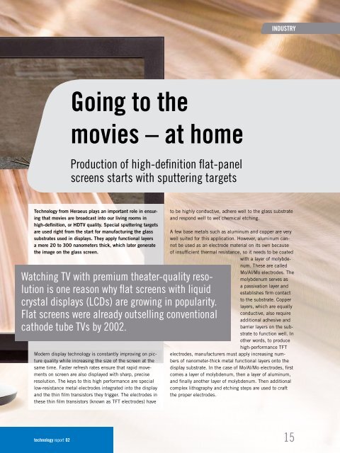
Going to the<br />
movies – at home<br />
Production of high-definition flat-panel<br />
screens starts with sputtering targets<br />
Technology from Heraeus plays an important role in ensuring<br />
that movies are broadcast into our living rooms in<br />
high-definition, or HDTV quality. Special sputtering targets<br />
are used right from the start for manufacturing the glass<br />
substrates used in displays. They apply functional layers<br />
a mere 20 to 300 nanometers thick, which later generate<br />
the image on the glass screen.<br />
Watching TV with premium theater-quality resolution<br />
is one reason why flat screens with liquid<br />
crystal displays (LCDs) are growing in popularity.<br />
Flat screens were already outselling conventional<br />
cathode tube TVs by 2002.<br />
Modern display technology is constantly improving on picture<br />
quality while increasing the size of the screen at the<br />
same time. Faster refresh rates ensure that rapid movements<br />
on screen are also displayed with sharp, precise<br />
resolution. The keys to this high performance are special<br />
low-resistance metal electrodes integrated into the display<br />
and the thin film transistors they trigger. The electrodes in<br />
these thin film transistors (known as TFT electrodes) have<br />
INDUSTRY<br />
to be highly conductive, adhere well to the glass substrate<br />
and respond well to wet chemical etching.<br />
A few base metals such as aluminum and copper are very<br />
well suited for this application. However, aluminum cannot<br />
be used as an electrode material on its own because<br />
of insufficient thermal resistance, so it needs to be coated<br />
with a layer of molybdenum.<br />
These are called<br />
Mo/Al/Mo electrodes. The<br />
molybdenum serves as<br />
a passivation layer and<br />
establishes firm contact<br />
to the substrate. Copper<br />
layers, which are equally<br />
conductive, also require<br />
additional adhesive and<br />
barrier layers on the substrate<br />
to function well. In<br />
other words, to produce<br />
high-performance TFT<br />
electrodes, manufacturers must apply increasing numbers<br />
of nanometer-thick metal functional layers onto the<br />
display substrate. In the case of Mo/Al/Mo electrodes, first<br />
comes a layer of molybdenum, then a layer of aluminum,<br />
and finally another layer of molybdenum. Then additional<br />
complex lithography and etching steps are used to craft<br />
the proper electrodes.<br />
15