An Optical Demonstration of Fractal Geometry - Materials Science ...
An Optical Demonstration of Fractal Geometry - Materials Science ...
An Optical Demonstration of Fractal Geometry - Materials Science ...

You also want an ePaper? Increase the reach of your titles
YUMPU automatically turns print PDFs into web optimized ePapers that Google loves.
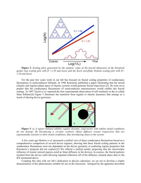
Figure 2: Scaling plots generated by the analytic value <strong>of</strong> the fractal dimension <strong>of</strong> the Sierpinsk<br />
gasket (top scaling plot with D =1.58 and inset) and the Koch snowflake (bottom scaling plot with D=<br />
1.26 and inset).<br />
For the past few years work in our lab has focused on fractal scaling properties <strong>of</strong> conductance<br />
fluctuations in semiconductor billiards. In 1996 Ketzmeric published a paper illustrating that the mixed<br />
(chaotic and regular) phase space <strong>of</strong> chaotic systems would generate fractal trajectories.[3] He went on to<br />
predict that the conductance fluctuations <strong>of</strong> semiconductor nanostructures would exhibit this fractal<br />
scaling. In 1997 Taylor et al. reported the first experimental observation <strong>of</strong> self similarity in the so called<br />
Sinai billiard.[4] Figure 3 illustrates the transition from regular to chaotic dynamics that emerge as a<br />
result <strong>of</strong> altering device geometry.<br />
Figure 3: a) A square billiard exhibits regular dynamic, trajectories with similar initial conditions<br />
do not diverge. B) Introducing a circular scatterer (Sinai diffuser) creates trajectories that are<br />
exponentially sensitive to their initial conditions, thus introducing chaos to the system.<br />
A few years ago Marlow et al. presented a unified view <strong>of</strong> these conductance fluctuations based on a<br />
comprehensive comparison <strong>of</strong> several device regimes, showing that these fractal scaling patterns in the<br />
conductance fluctuations were not dependent on the device geometry or scattering regime properties that<br />
Ketzmeric’s proposal did not explain.[5] We <strong>of</strong>fered a unified model, proposing that the electrostatic<br />
influence <strong>of</strong> remote ionized regions acted as Sinai diffusers in the devices. In essence, the fractal patterns<br />
resulted from the device walls allowing repeated reflection <strong>of</strong>f <strong>of</strong> the diffusers, iterated chaos akin to the<br />
IFS mentioned above.<br />
Coupling this idea with our lab’s dedication to physics education, we set out to develop a simple<br />
demonstration <strong>of</strong> this phenomenon suitable for use in the classroom. Intrigued by the apparatus described