Memory - Vodafone Chair Mobile Communications Systems
Memory - Vodafone Chair Mobile Communications Systems
Memory - Vodafone Chair Mobile Communications Systems

Create successful ePaper yourself
Turn your PDF publications into a flip-book with our unique Google optimized e-Paper software.
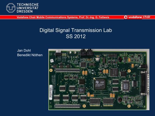
<strong>Vodafone</strong> <strong>Chair</strong> <strong>Mobile</strong> <strong>Communications</strong> <strong>Systems</strong>, Prof. Dr.-Ing. G. Fettweis<br />
Jan Dohl<br />
Benedikt Nöthen<br />
Digital Signal Transmission Lab<br />
SS 2012<br />
chair
<strong>Vodafone</strong> <strong>Chair</strong><br />
Tomahawk (Jan. 2008) Tomahawk2 (2012)<br />
Möglichkeiten für Studenten:<br />
Studienarbeit<br />
Diplomarbeit<br />
SHK (8,28 Euro)<br />
Ansprechpartner<br />
- Hardware<br />
- Software<br />
Oliver Arnold (oliver.arnold@ifn.et.tu-dresden.de)<br />
- Simulation<br />
- Verifikation<br />
Steffen Kunze (steffen.kunze@ifn.et.tu-dresden.de)<br />
chair<br />
TU Dresden, 6/4/2012 Slide 2
Termine<br />
05. Juni: Einführungsveranstaltung (BAR II/63a)<br />
07. Juni: kurzer Test (BAR IV/1)<br />
Versuche: Jeweils Dienstag,14:50 Uhr, Bar IV/1<br />
12. Juni: Versuch 1: Realisierung eines Echos in Audiodaten<br />
19. Juni: Versuch 2: Abtastratenerhöhung<br />
26. Juni: Versuch 3: Synchronisation und Decodierung<br />
03. Juli: Versuch 4: Realisierung einer 16-QAM Übertragungsstrecke<br />
E-Mail-Verteiler<br />
chair<br />
TU Dresden, 6/4/2012 Slide 3
Introduction<br />
Hardware<br />
Why to use digital signal processing?<br />
General introduction to DSPs<br />
The TMS320C6455 DSP<br />
Architecture Overview<br />
Peripherals<br />
DSK6455 evaluation board - Software<br />
Code Composer Studio<br />
DSP/BIOS<br />
Multi-channel Buffered Serial Port (McBSP)<br />
chair<br />
TU Dresden, 6/4/2012 Slide 4
Hardware<br />
chair<br />
TU Dresden, 6/4/2012 Slide 5
Digital Signal Processing (DSP)<br />
Wireless / Cellular<br />
Voice-band audio<br />
RF codecs<br />
Voltage regulation<br />
Consumer Audio<br />
Stereo A/D, D/A<br />
PLL<br />
Mixers<br />
Multimedia<br />
Stereo audio<br />
Imaging<br />
Graphics palette<br />
Voltage regulation<br />
DSP:<br />
Technology<br />
Enabler<br />
HDD<br />
PRML read channel<br />
MR pre-amp<br />
Servo control<br />
SCSI tranceivers<br />
DTAD<br />
Speech synthesizer<br />
Mixed-signal<br />
processor<br />
chair<br />
Automotive<br />
Digital radio A/D/A<br />
Active suspension<br />
Voltage regulation<br />
TU Dresden, 6/4/2012 Slide 6
System Considerations<br />
Size<br />
Interfacing<br />
Ease-of Use<br />
• Programming<br />
• Interfacing<br />
• Debugging<br />
Performance<br />
Cost<br />
• Device cost<br />
• System cost<br />
• Development cost<br />
• Time to market<br />
Power<br />
Integration<br />
• <strong>Memory</strong><br />
• Peripherals<br />
chair<br />
TU Dresden, 6/4/2012 Slide 7
Why Go Digital?<br />
Easier<br />
Digital signal processing techniques are now so<br />
powerful that sometimes it is extremely difficult, if<br />
not impossible, for analogue signal processing to<br />
achieve similar performance.<br />
Examples:<br />
FIR filter with linear phase<br />
Adaptive filters<br />
chair<br />
TU Dresden, 6/4/2012 Slide 8
Why Go Digital?<br />
Analogue signal processing is achieved by<br />
using analogue components such as:<br />
Resistors<br />
Capacitors<br />
Inductors<br />
Inherent tolerances:<br />
Temperature<br />
Voltage changes<br />
Mechanical vibrations<br />
chair<br />
TU Dresden, 6/4/2012 Slide 9
Why Go Digital?<br />
With DSP? - It is easy to:<br />
Change applications<br />
Correct applications<br />
Update applications<br />
Additionally DSPs reduce:<br />
Noise susceptibility<br />
Chip count<br />
Development time<br />
Cost<br />
Power consumption<br />
chair<br />
TU Dresden, 6/4/2012 Slide 10
General Introduction to DSPs<br />
chair<br />
TU Dresden, 6/4/2012 Slide 11
What Problem Are We Trying To Solve?<br />
Digital sampling of<br />
an analog signal:<br />
A<br />
ADC<br />
t<br />
x Y<br />
DSP<br />
Most DSP algorithms can be<br />
expressed as:<br />
count<br />
DAC<br />
Y = Σ ai * xi i = 1<br />
for (i = 1; i < count; i++){<br />
sum += m[i] * n[i]; }<br />
chair<br />
TU Dresden, 6/4/2012 Slide 12
What are the typical DSP algorithms?<br />
The Sum of Products (SOP) is the key element in<br />
most DSP algorithms:<br />
Algorithm Equation<br />
Finite Impulse Response Filter<br />
Infinite Impulse Response Filter<br />
Convolution<br />
Discrete Fourier Transform<br />
Discrete Cosine Transform<br />
yn ( ) = a xn ( − k)<br />
chair<br />
TU Dresden, 6/4/2012 Slide 13<br />
y(<br />
n)<br />
=<br />
F<br />
M<br />
∑<br />
k=<br />
0<br />
a<br />
k<br />
y(<br />
n)<br />
=<br />
∑ − N 1<br />
n=<br />
0<br />
M<br />
∑<br />
k = 0<br />
k<br />
x(<br />
n − k)<br />
+<br />
N<br />
∑<br />
k=<br />
0<br />
N<br />
∑<br />
k=<br />
1<br />
b<br />
k<br />
x(<br />
k)<br />
h(<br />
n − k)<br />
y(<br />
n − k)<br />
X ( k)<br />
= x(<br />
n)<br />
exp[ − j(<br />
2π<br />
/ N)<br />
nk]<br />
∑ − N 1<br />
x=<br />
0<br />
⎡ π<br />
⎢<br />
⎣2N<br />
( u)<br />
= c(<br />
u).<br />
f ( x).<br />
cos u(<br />
2x<br />
+ 1)<br />
⎤<br />
⎥<br />
⎦
Why do we need DSP processors?<br />
Use a DSP processor when the following<br />
are required:<br />
Cost saving<br />
Smaller size<br />
Low power consumption<br />
Processing of many “high” frequency signals in<br />
real-time<br />
Use a GPP processor when the following<br />
are required:<br />
Large memory<br />
Advanced operating systems<br />
chair<br />
TU Dresden, 6/4/2012 Slide 14
Hardware vs. Microcode multiplication<br />
DSP processors are optimized to perform<br />
multiplication and addition operations.<br />
Multiplication and addition are done in<br />
hardware and in one cycle.<br />
Example: 4-bit multiply (unsigned).<br />
Hardware Microcode<br />
1011<br />
x 1110<br />
1011<br />
x 1110<br />
10011010 0000<br />
1011.<br />
1011..<br />
1011...<br />
10011010<br />
Cycle 1<br />
Cycle 2<br />
Cycle 3<br />
Cycle 4<br />
Cycle 5<br />
chair<br />
TU Dresden, 6/4/2012 Slide 15
General Purpose DSP vs. DSP in ASIC<br />
Application Specific Integrated Circuits<br />
(ASICs) are semiconductors designed for<br />
dedicated functions.<br />
The advantages and disadvantages of using<br />
ASICs are listed below:<br />
Advantages<br />
• High throughput<br />
• Lower silicon area<br />
• Lower power consumption<br />
• Improved reliability<br />
• Reduction in system noise<br />
• Low overall system cost<br />
Disadvantages<br />
• High investment cost<br />
• Less flexibility<br />
• Long time from design to<br />
market<br />
chair<br />
TU Dresden, 6/4/2012 Slide 16
Floating vs. Fixed point processors<br />
Applications which require:<br />
High precision<br />
Wide dynamic range<br />
High signal-to-noise ratio<br />
Ease of use<br />
Need a floating point processor<br />
Drawback of floating point processors:<br />
Higher power consumption<br />
Usually higher cost<br />
Usually slower than fixed-point counterparts and<br />
larger in size<br />
chair<br />
TU Dresden, 6/4/2012 Slide 17
TMS320C6455 Architectural Overview<br />
chair<br />
TU Dresden, 6/4/2012 Slide 18
General DSP System Block Diagram<br />
External<br />
<strong>Memory</strong><br />
Internal <strong>Memory</strong><br />
Internal Buses<br />
Central<br />
Processing<br />
Unit<br />
chair<br />
TU Dresden, 6/4/2012 Slide 19<br />
P<br />
E<br />
R<br />
I<br />
P<br />
H<br />
E<br />
R<br />
A<br />
L<br />
S
‘6455 CPU Overview<br />
Specification<br />
Clock Rate: 1/1.2 GHz 9600 MIPS<br />
0.09-μm/7-Level Metal Process – CMOS Technology<br />
CPU has got two Datapaths, altogether:<br />
2* .M,<br />
2* .L,<br />
2*.S,<br />
2*.D<br />
2* 32 32-Bit General-Purpose Registers<br />
chair<br />
TU Dresden, 6/4/2012 Slide 20
‘6455 CPU Overview<br />
VelociTI advanced very-long instruction words (VLIW)<br />
Program <strong>Memory</strong> Width is 256 Bit<br />
Up to 8 32-Bit instructions can be executed in parallel/Cycle<br />
16, 32 and 40 bit fixed point operands<br />
Instruction parallelism is detected at compile-time<br />
no data dependency checking is done in Hardware.<br />
Instruction Packing Reduces Code Size<br />
All operations work on registers<br />
<strong>Memory</strong> Architecture<br />
32K-Byte L1P Program Cache (Direct Mapped)<br />
32K-Byte L1D Data Cache (2-Way Set-Associative)<br />
2048K-Byte L2 Unified Mapped RAM/L2 Cache (Flexible<br />
Data/Program Allocation)<br />
chair<br />
TU Dresden, 6/4/2012 Slide 21
Functional Block and CPU Diagram<br />
chair<br />
TU Dresden, 6/4/2012 Slide 22
A ‘6455 Datapath<br />
.S & .L<br />
.M<br />
.D<br />
Arithmetic, Logical<br />
& Branch functions<br />
Multiply, Rotation,<br />
Bit expansion<br />
Data-addressing<br />
Only way to access<br />
memory<br />
Cross path<br />
chair<br />
TU Dresden, 6/4/2012 Slide 23
Functional Units and Operations Performed<br />
Functional Unit Fixed-Point Operations<br />
.L unit (.L1, .L2) 32/40-bit arithmetic and compare operations,<br />
32-bit logical operations,<br />
Leftmost 1 or 0 counting for 32 bits,<br />
Byte shifts, 5-bit constant generation<br />
.S unit (.S1, .S2) 32-bit arithmetic operations,<br />
32/40-bit shifts and 32-bit bit field operations,<br />
32-bit logical operations, Branches, Byte shifts,<br />
Register transfer to/from control register file (.S2 only)<br />
.M unit (.M1, .M2) 32x32-bit multiply, 16x16-bit multiply, 16x32-bit multiply,<br />
rotation, variable shift operations<br />
.D unit (.D1, .D2) 32-bit add, substract, linear and circular address calculation<br />
32-bit logical operations, 5-bit constant generation,<br />
Loads and stores 5-bit/15-bit constant offset<br />
chair<br />
TU Dresden, 6/4/2012 Slide 24
C6400: Instruction Set<br />
.S<br />
.L<br />
.D<br />
.M<br />
ADD<br />
ADDK<br />
ADD2<br />
AND<br />
B<br />
CLR<br />
EXT<br />
MV<br />
MVC<br />
MVK<br />
MVKH<br />
.S Unit<br />
NEG<br />
NOT<br />
OR<br />
SET<br />
SHL<br />
SHR<br />
SSHL<br />
SUB<br />
SUB2<br />
XOR<br />
ZERO<br />
ADD<br />
ADDAB (B/H/W)<br />
LDB (B/H/W)<br />
LDDW<br />
MV<br />
.D Unit<br />
ABSSP<br />
ABSDP<br />
CMPGTSP<br />
CMPEQSP<br />
CMPLTSP<br />
CMPGTDP<br />
CMPEQDP<br />
CMPLTDP<br />
RCPSP<br />
RCPDP<br />
RSQRSP<br />
RSQRDP<br />
SPDP<br />
NEG<br />
STB (B/H/W)<br />
SUB<br />
SUBAB (B/H/W)<br />
ZERO<br />
ABS<br />
ADD<br />
AND<br />
CMPEQ<br />
CMPGT<br />
CMPLT<br />
LMBD<br />
MV<br />
NEG<br />
NORM<br />
MPY<br />
MPYH<br />
MPYLH<br />
MPYHL<br />
No Unit Used<br />
IDLE<br />
chair<br />
TU Dresden, 6/4/2012 Slide 25<br />
NOP<br />
.L Unit<br />
NOT<br />
OR<br />
SADD<br />
SAT<br />
SSUB<br />
SUB<br />
SUBC<br />
XOR<br />
ZERO<br />
.M Unit<br />
SMPY<br />
SMPYH<br />
ADDSP<br />
ADDDP<br />
SUBSP<br />
SUBDP<br />
INTSP<br />
INTDP<br />
SPINT<br />
DPINT<br />
SPRTUNC<br />
DPTRUNC<br />
DPSP<br />
MPYSP<br />
MPYDP<br />
MPYI<br />
MPYID
'C6x System Block Diagram<br />
Ext’l<br />
<strong>Memory</strong><br />
- Sync<br />
- Async<br />
Addr<br />
D (32)<br />
EMIF<br />
Program<br />
RAM<br />
Regs (A0-A31)<br />
Internal Buses<br />
.D1<br />
.M1<br />
.L1<br />
.S1<br />
.D2<br />
.M2<br />
CPU<br />
chair<br />
TU Dresden, 6/4/2012 Slide 26<br />
.L2<br />
.S2<br />
Control Regs<br />
Regs (B0-B31)<br />
Data Ram<br />
DMA<br />
Serial Port<br />
Host Port<br />
Boot Load<br />
Timers<br />
Pwr Down
chair<br />
TU Dresden, 6/4/2012 Slide 27
‘C6455 <strong>Memory</strong> Map<br />
chair<br />
TU Dresden, 6/4/2012 Slide 28
How are Peripherals Controlled?<br />
Control and configuration of internal peripherals is done<br />
by memory mapped control registers<br />
Example of Timer mode control register:<br />
31<br />
7<br />
HLD<br />
6<br />
GO<br />
Rsvd<br />
5<br />
Rsvd<br />
4<br />
PWID<br />
12<br />
TSAT<br />
DATIN<br />
INVIMP<br />
DATOUT<br />
CLKSRC<br />
INVOUT<br />
chair<br />
TU Dresden, 6/4/2012 Slide 30<br />
11<br />
3<br />
10<br />
2<br />
9<br />
1<br />
8<br />
C/P<br />
0<br />
Func
Operands<br />
Operands can be<br />
5-bit constants (or 16-bit in some special instruct.)<br />
32-bit Registers<br />
40-bit Registers<br />
64-bit Registers<br />
A 40-bit or a 64-bit register can be obtained by<br />
concatenating two registers<br />
The registers must be from the same side<br />
The first register must be even and the second odd (e.g.<br />
A1:A0, B9:B8 or A15:A14)<br />
The registers must be consecutive<br />
chair<br />
TU Dresden, 6/4/2012 Slide 31
Conditional execution<br />
All instructions in each Functional Unit of both Data<br />
paths can be executed conditionally<br />
Only the Registers A1, A2, B0, B1, B2 can hold the<br />
condition<br />
Conditional Execution uses the Syntax<br />
e.g<br />
[!condition] Instruction<br />
[!B0] ADD.L1 A1,A2,A3 ; add if B0 ==0<br />
[B0] ADD.L1 A1,A2,A3 ; add if B0 != 0<br />
chair<br />
TU Dresden, 6/4/2012 Slide 32
Branches<br />
Branches are required to realize loops and change<br />
the program flow<br />
Branches are very useful in conjunction with<br />
conditional execution<br />
There are two branch types supported:<br />
Relative Branching<br />
Absolute Branching<br />
chair<br />
TU Dresden, 6/4/2012 Slide 33
More on the Branch Instruction (1)<br />
With this processor all the instructions are encoded<br />
in a 32-bit.<br />
Therefore the label must have a dynamic range of<br />
less than 32-bit as the instruction B has to be<br />
coded.<br />
B<br />
Case 1: B .S1 label<br />
Relative branch.<br />
32-bit<br />
21-bit relative address<br />
Label limited to +/- 2 20 offset.<br />
chair<br />
TU Dresden, 6/4/2012 Slide 34
More on the Branch Instruction (2)<br />
By specifying a register as an operand instead of<br />
a label, it is possible to have an absolute branch.<br />
This will allow a dynamic range of 2 32 .<br />
Case 2: B .S2 register<br />
B<br />
Absolute branch.<br />
32-bit<br />
Operates on .S2 ONLY!<br />
5-bit register<br />
code<br />
chair<br />
TU Dresden, 6/4/2012 Slide 35
Getting Data from the <strong>Memory</strong><br />
All Instructions work exclusively on Registers<br />
The .D Units in the Data-Paths are used to load and<br />
store the required Data from and to the <strong>Memory</strong><br />
Load and Store Instructions use an Address<br />
operator X:<br />
chair<br />
TU Dresden, 6/4/2012 Slide 36
Addressing Modes<br />
There are two addressing modes supported:<br />
Linear Addressing<br />
Circular Addressing (e.g. Convolution)<br />
Circular Addressing supports block sizes 2 N<br />
Only the lower N bits of the Address are modified by address<br />
arithmetic. This equals mod(2 N ) operations.<br />
The addressing mode is selected by control register<br />
„AMR‘<br />
Operands for CA are limited to A4-A7, B4-B7<br />
chair<br />
TU Dresden, 6/4/2012 Slide 37
Floating vs. Fixed point processors<br />
Fixed point arithmetic<br />
16-bit (integer or fractional)<br />
Signed or unsigned<br />
Floating point arithmetic<br />
32-bit single precision<br />
64-bit single precision<br />
Using signed and unsigned integers:<br />
Multiplication overflow.<br />
Addition overflow<br />
Saturate the result<br />
Double precision result<br />
Fractional arithmetic<br />
( n)<br />
= a(<br />
k)<br />
x(<br />
n − k)<br />
e.g. If A and B are fractional then: A x B < min(A, B)<br />
chair<br />
TU Dresden, 6/4/2012 Slide 38<br />
y<br />
∑ − N 1<br />
k = 0
C6000 C Data Types<br />
Type Size Representation<br />
char, signed char 8 bits ASCII<br />
unsigned char 8 bits ASCII<br />
short 16 bits 2’s complement<br />
unsigned short 16 bits binary<br />
int, signed int 32 bits 2s complement<br />
unsigned int 32 bits binary<br />
long, signed long 40 bits 2’s complement<br />
unsigned long 40 bits binary<br />
enum 32 bits 2’s complement<br />
float 32 bits IEEE 32-bit<br />
double 64 bits IEEE 64-bit<br />
long double 64 bits IEEE 64-bit<br />
pointers 32 bits binary<br />
chair<br />
TU Dresden, 6/4/2012 Slide 39
Numerical Issues - Useful Tips<br />
Multiply by 2: Use shift left<br />
Divide by 2: Use shift right<br />
Log 2N: Use shift<br />
Sine, Cosine, Log: Use look up tables<br />
To convert a fractional number to hex:<br />
Num x 2 15<br />
Then convert to hex<br />
e.g: convert 0.5 to hex<br />
0.5 x 2 15 = 16384<br />
(16384) dec = (0x4000) hex<br />
chair<br />
TU Dresden, 6/4/2012 Slide 40
Numerical Issues - 32-bit Multiplication<br />
It is possible to perform 32-bit multiplication<br />
using 16-bit multipliers.<br />
Example: c = a x b (with 32-bit values).<br />
a =<br />
b =<br />
a h<br />
b h<br />
32-bits<br />
a * b = (a h
Selected ‘6455 Peripherals<br />
chair<br />
TU Dresden, 6/4/2012 Slide 42
C6000 Peripherals<br />
Host µC<br />
External<br />
<strong>Memory</strong><br />
XB<br />
Host Port<br />
PCI<br />
16/32 EMIF<br />
McBSPs<br />
EDMA<br />
DMA<br />
Boot Loader<br />
Timer/Count<br />
PLL<br />
Internal Buses<br />
.D1<br />
.M1<br />
.L1<br />
.S1<br />
.D2<br />
.M2<br />
.L2<br />
.S2<br />
chair<br />
TU Dresden, 6/4/2012 Slide 43<br />
Regs (A0-A15/31)<br />
Internal<br />
<strong>Memory</strong><br />
CPU<br />
Regs (B0-B15/31)
The McBSP<br />
Multichannel Buffered Serial Port<br />
Up to 100 Mb/sec performance<br />
full-duplex, synchronous serial-ports<br />
Enables direct interfacing to industry standard<br />
Codecs, Analog interface Chips and other serially<br />
connected devices<br />
Supports a wide range of data-sizes, including 8, 12,<br />
16, 20, 24 and 32 bits<br />
Bit, Word(channel), Frame<br />
In our lab the McBSP is used to connect to the A/D,<br />
D/A<br />
chair<br />
TU Dresden, 6/4/2012 Slide 44
ADC/DAC<br />
24-bit resolution<br />
Multiple Digital Transfer widths (16-,20-, 24-, 32-bits)<br />
SAMPLING RATE: Up to 96kHz<br />
chair<br />
TU Dresden, 6/4/2012 Slide 45
What is the bootloader?<br />
VCC<br />
EPROM<br />
VCC<br />
EMIF<br />
DMA<br />
C6211/C6711<br />
Boot Config<br />
When the DSP is NOT powered or under<br />
reset the internal program memory is in a<br />
random state.<br />
chair<br />
TU Dresden, 6/4/2012 Slide 46<br />
L2 Cache<br />
L1P Cache<br />
CPU<br />
L1D Cache<br />
Addr<br />
0000<br />
0001<br />
0002<br />
0003<br />
...
What is the bootloader?<br />
VCC<br />
EPROM<br />
VCC<br />
EMIF<br />
DMA<br />
C6211/C6711<br />
Boot Config<br />
When the DSP is powered and the CPU is taken out of<br />
reset the internal memory is still in a random state and<br />
the program will start running for address zero.<br />
chair<br />
TU Dresden, 6/4/2012 Slide 47<br />
L2 Cache<br />
L1P Cache<br />
CPU<br />
PC=0000 PC=0001 PC=0002 PC=0003<br />
L1D Cache<br />
Addr<br />
0000<br />
0001<br />
0002<br />
0003<br />
...
What is the bootloader?<br />
VCC<br />
EPROM<br />
VCC<br />
EMIF<br />
DMA<br />
C6211/C6711<br />
Boot Config<br />
With the boot, a portion of code can be<br />
automatically copied from external to internal<br />
memory.<br />
chair<br />
TU Dresden, 6/4/2012 Slide 48<br />
L2 Cache<br />
L1P Cache<br />
CPU<br />
L1D Cache
Interrupts<br />
DSPs must be able to execute tasks on<br />
asynchronous events<br />
Interrupts suspend the current processor task<br />
and save its context<br />
A interrupt service routine (ISR) is executed<br />
After completion of the ISR, the context of the<br />
former task is restored and the execution<br />
continues<br />
Interrupts are organized hierarchically<br />
vs. Polling<br />
chair<br />
TU Dresden, 6/4/2012 Slide 49
Interrupt Interrupt- and Thread Types<br />
HWI priorities set by hardware<br />
One ISR per interrupt<br />
14 SWI priority levels Multiple<br />
SWIs at each level<br />
15 TSK priority levels Multiple<br />
TSKs at each level<br />
Multiple IDL functions<br />
Continuous loop<br />
chair<br />
HWI triggered by hardware interrupt<br />
IDL runs as the background thread<br />
TU Dresden, 6/4/2012 Slide 50
The DSK6455 Development Kit<br />
chair<br />
TU Dresden, 6/4/2012 Slide 51
Code Composer Studio and the DSK<br />
chair<br />
TU Dresden, 6/4/2012 Slide 52
Code Composer Studio<br />
The Code Composer Studio (CCS) application<br />
provides an integrated environment with the<br />
following capabilities:<br />
Integrated development environment with an editor,<br />
debugger, project manager, profiler, etc.<br />
‘C/C++’ compiler, assembly optimiser and linker<br />
(code generation tools).<br />
Simulator.<br />
Real-time operating system (DSP/BIOS).<br />
Real-Time Data Exchange (RTDX) between the<br />
Host and Target.<br />
Real-time analysis and data visualisation.<br />
chair<br />
TU Dresden, 6/4/2012 Slide 53
Hardware: (2) DSK Connections<br />
(A) Parallel port: The PC’s USB port is connected to the DSK.<br />
USB<br />
PC DSK<br />
Power<br />
Supply<br />
Line-level Output<br />
Line-level Input<br />
(B) JTAG: An XDS JTAG emulator connected to the PC (either<br />
internal or external) is connected to the JTAG header on the DSK.<br />
JTAG<br />
PC DSK<br />
XDS<br />
Power<br />
Supply<br />
External<br />
Power<br />
Supply<br />
External<br />
Power<br />
Supply<br />
Line-level Output<br />
Line-level Input<br />
chair<br />
TU Dresden, 6/4/2012 Slide 54
Laboratory Exercise: Using CCS<br />
chair<br />
TU Dresden, 6/4/2012 Slide 55
Laboratory Exercise: Using CCS<br />
Click on Project properties<br />
Add include search paths:<br />
"C:\ti\ccsv5\dsk6455_v2\boards\dsk6455_v2\csl_c64xplus_intc\inc"<br />
"C:\ti\ccsv5\dsk6455_v2\boards\dsk6455_v2\csl_c6455\inc"<br />
"C:\ti\ccsv5\dsk6455_v2\boards\dsk6455_v2\include"<br />
chair<br />
TU Dresden, 6/4/2012 Slide 57
Laboratory Exercise: Using CCS<br />
Add Library files to be included:<br />
"C:\ti\ccsv5\dsk6455_v2\boards\dsk6455_v2\lib\dsk6455bsl\dsk6455bsl.lib"<br />
"C:\ti\ccsv5\dsk6455_v2\boards\dsk6455_v2\csl_c6455\lib\csl_c6455.lib"<br />
Add Library search paths:<br />
"C:\ti\ccsv5\dsk6455_v2\boards\dsk6455_v2\lib\dsk6455bsl"<br />
"C:\ti\ccsv5\dsk6455_v2\boards\dsk6455_v2\csl_c6455\lib"<br />
chair<br />
TU Dresden, 6/4/2012 Slide 58
DSP/BIOS<br />
chair<br />
TU Dresden, 6/4/2012 Slide 59
DSP/BIOS Components<br />
The user writes code (‘C’/assembly) using the DSP/BIOS library.<br />
The user can use the configuration tools to setup the system.<br />
All the files generated constitute a project.<br />
chair<br />
TU Dresden, 6/4/2012 Slide 60
DSP/BIOS Components<br />
The project is then compiled, assembled and linked by the code<br />
generation tools in order to generate an executable file (*.out).<br />
There are also some DSP/BIOS plug-ins that can be used, for<br />
instance, as program test while the target is running.<br />
chair<br />
TU Dresden, 6/4/2012 Slide 61
Graphical Interface for Static System<br />
Setup<br />
The DSP/BIOS main objects are:<br />
chair<br />
(1) Hardware interrupts (HWI).<br />
(2) Software interrupts (SWI).<br />
(3) Tasks (TSK, IDL).<br />
(4) Data and I/O streams (RTDX, SIO, PIP, HST).<br />
(5) Synchronisation and Communication (SEM, MBX,<br />
LCK).<br />
(6) Timing (PRD, CLK).<br />
(7) Logging and statistics (LOG, STS, TRC).<br />
For a complete list see: \Links\SPRU303.pdf (Page 1-5).<br />
TU Dresden, 6/4/2012 Slide 62
Project Configurations<br />
Right Click on Project new target<br />
Configuration file<br />
Open Configuration file and select: DSK6455<br />
chair<br />
TU Dresden, 6/4/2012 Slide 63
Project Configurations<br />
Right click->new->others<br />
Select DSP/BIOS v5x configuration file<br />
chair<br />
TU Dresden, 6/4/2012 Slide 64
Project Configurations<br />
DSP/BIOS configuration window opens<br />
automatically: select DSK6455<br />
chair<br />
TU Dresden, 6/4/2012 Slide 65
Project Configurations<br />
Open the tcf File:<br />
»<br />
• Right click SWI->insert swi-> name it Process Buffer Swi<br />
• Right click process buffer swi<br />
chair<br />
TU Dresden, 6/4/2012 Slide 66
Multi-channel Buffered Serial Port (McBSP)<br />
chair<br />
TU Dresden, 6/4/2012 Slide 67
Objectives<br />
Definition of Terms:<br />
Bit, word or channel, frame and phase.<br />
Understand basic serial port operation.<br />
Understand clock generation.<br />
Pin polarity.<br />
Serial port interrupts.<br />
Describe multi-channel operation.<br />
Programming the serial port.<br />
chair<br />
TU Dresden, 6/4/2012 Slide 68
Basic Definitions: Bits, Words ?<br />
CLK<br />
FS<br />
Data<br />
Data<br />
a1 a0<br />
Serial Port<br />
SP Ctrl (SPCR)<br />
Rcv Ctrl (RCR)<br />
Xmt Ctrl (XCR)<br />
Rate (SRGR)<br />
Pin Ctrl (PCR)<br />
Bit<br />
b7 b6 b5 b4 b3 b2 b1 b0<br />
Word<br />
chair<br />
“Bit” - one data bit per SP clock period.<br />
“Word” or “channel” contains #bits specified by<br />
WDLEN1 (8, 12, 16, 20, 24, 32).<br />
7 5<br />
RWDLEN1<br />
7 5<br />
XWDLEN1<br />
TU Dresden, 6/4/2012 Slide 69
Basic Definitions: Frame?<br />
FS<br />
ata<br />
w6 w7<br />
Serial Port<br />
SP Ctrl (SPCR)<br />
Rcv Ctrl (RCR)<br />
Xmt Ctrl (XCR)<br />
Rate (SRGR)<br />
Pin Ctrl (PCR)<br />
Word<br />
w0 w1 w2 w3 w4 w5 w6 w7<br />
Frame<br />
“Frame” - contains one or multiple words.<br />
FRLEN1 specifies #words per frame (1-128).<br />
RFRLEN1<br />
RWDLEN1<br />
chair<br />
TU Dresden, 6/4/2012 Slide 70<br />
14<br />
14<br />
8<br />
8<br />
XFRLEN1<br />
7<br />
7<br />
5<br />
5<br />
XWDLEN1
Objectives<br />
Definition of Terms:<br />
Bit, word or channel, frame and phase.<br />
Understand basic serial port operation.<br />
Understand clock generation.<br />
Pin polarity.<br />
Serial port interrupts.<br />
Describe multi-channel operation.<br />
Programming the serial port.<br />
chair<br />
TU Dresden, 6/4/2012 Slide 74
Serial Port - Basic Operation<br />
DR<br />
DX<br />
CLKR<br />
CLKX<br />
FSR<br />
FSX<br />
Multi-Channel Buffered<br />
Serial Port (McBSP)<br />
RSR RBR<br />
DRR<br />
XSR<br />
Serial Port<br />
Control Logic<br />
SPCR RCR<br />
Peripheral Bus<br />
SRGR<br />
XCR PCR<br />
DXR<br />
chair<br />
TU Dresden, 6/4/2012 Slide 75<br />
P<br />
e<br />
r<br />
i<br />
p<br />
h<br />
B<br />
u<br />
s<br />
“TRANSMIT”<br />
“RECEIVE”<br />
CPU<br />
DMA
McBSP Registers<br />
Receive<br />
Transmit<br />
Control<br />
RSR Receive Shift Reg<br />
RBR Receive Buffer Reg<br />
DRR Data Receive Reg<br />
XSR Transmit Shift Reg<br />
DXR Data Transmit Reg<br />
SPCR Serial Port Control Reg<br />
RCR Receive Control Reg<br />
XCR Transmit Control Reg<br />
SRGR Sample Rate Generator<br />
PCR Pin Control Reg<br />
MCR Multi-Channel Ctrl Reg<br />
RCER Rcv Channel Enable Reg<br />
XCER Xmit Channel Enable Reg<br />
chair<br />
TU Dresden, 6/4/2012 Slide 76
Objectives<br />
Definition of Terms:<br />
Bit, word or channel, frame and phase.<br />
Understand basic serial port operation.<br />
Understand clock generation.<br />
Pin polarity.<br />
Serial port status and interrupts.<br />
Describe multi-channel operation.<br />
Programming the serial port.<br />
chair<br />
TU Dresden, 6/4/2012 Slide 77
RRDY/XRDY Status and Interrupts<br />
RBR DRR<br />
XSR DXR<br />
Serial Port<br />
SP Ctrl (SPCR)<br />
Rcv Ctrl (RCR)<br />
Xmt Ctrl (XCR)<br />
Rate (SRGR)<br />
Pin Ctrl (PCR)<br />
RRDY=1<br />
“Ready to Read”<br />
XRDY=1<br />
“Ready to Write”<br />
CPU<br />
RINT<br />
XINT<br />
EDMA<br />
Sync<br />
XRDY<br />
RRDY/XRDY displays the<br />
“status” of the read and<br />
transmit ports:<br />
0: not ready.<br />
1: ready to read/write.<br />
There are 3 methods for<br />
detecting if data is ready:<br />
RRDY<br />
chair<br />
TU Dresden, 6/4/2012 Slide 78<br />
17<br />
Poll SPCR bits via s/w.<br />
Config CPU ints<br />
(RINT/XINT).<br />
Program DMA sync events.<br />
1
Next Steps<br />
Create a new C function:<br />
processData(Int16 *inBuf, Int16 outBuf, int16 length)<br />
Function will be called by HWI/SWI routine<br />
inBuf is pointer to samples of the in-Signal<br />
outBuf. is pointer to processed samples ready for<br />
audio out<br />
chair<br />
TU Dresden, 6/4/2012 Slide 79