Catalytic growth of semiconducting zinc oxide nanowires and their ...
Catalytic growth of semiconducting zinc oxide nanowires and their ...
Catalytic growth of semiconducting zinc oxide nanowires and their ...

You also want an ePaper? Increase the reach of your titles
YUMPU automatically turns print PDFs into web optimized ePapers that Google loves.
Journal <strong>of</strong> Crystal Growth 234 (2002) 171–175<br />
<strong>Catalytic</strong> <strong>growth</strong> <strong>of</strong> <strong>semiconducting</strong> <strong>zinc</strong> <strong>oxide</strong> <strong>nanowires</strong> <strong>and</strong><br />
<strong>their</strong> photoluminescence properties<br />
Abstract<br />
Y.W. Wang*, L.D. Zhang, G.Z. Wang, X.S. Peng, Z.Q. Chu, C.H. Liang<br />
Institute <strong>of</strong> Solid State Physics, Chinese Academy <strong>of</strong> Sciences, P.O. Box 1129, Hefei 230031, People’s Republic <strong>of</strong> China<br />
Received 23 May 2001; accepted 2 August 2001<br />
Communicated by R.S. Feigelson<br />
Semiconducting ZnO <strong>nanowires</strong> have been produced in bulk quantity by heating Zn powders (99.99%) containing<br />
Au nanoparticles at 9001C. Scanning electron microscopy <strong>and</strong> transmission electron microscopy observations show that<br />
the ZnO <strong>nanowires</strong> have diameters ranging from 30 to 60 nm <strong>and</strong> lengths up to several tens <strong>of</strong> micrometers. The <strong>growth</strong><br />
<strong>of</strong> ZnO <strong>nanowires</strong> is controlled by the conventional vapor–liquid–solid (VLS) mechanism. A green light emission was<br />
observed at room temperature, which could be attributed to the singly ionized oxygen vacancy formed in the ZnO<br />
<strong>nanowires</strong>. r 2002 Elsevier Science B.V. All rights reserved.<br />
PACS: 73.61.Tm; 78.40.Fy; 78.60.Ya<br />
Keywords: A1. Characterization; B1. Nanomaterials; B2. Semiconducting materials<br />
1. Introduction<br />
Quasi one-dimensional nanostructured materials<br />
such as nanotubes or <strong>nanowires</strong> have been<br />
successfully synthesized <strong>and</strong> have received much<br />
attention due to <strong>their</strong> peculiar physical properties<br />
<strong>and</strong> potential application in nanodevices [1].<br />
Considerable effort has been placed on the bulk<br />
synthesis <strong>of</strong> nanotubes or <strong>nanowires</strong> using laser<br />
ablation [2–4], template [5], solution [6], <strong>and</strong> other<br />
methods [7]. Most <strong>of</strong> these works, which focused<br />
on semiconductor systems such as Si [1], GaN [8],<br />
GaAs [9], have been investigated in detail. Over<br />
*Corresponding author. Fax: +86-551-559-1434.<br />
E-mail address: ywwangcn@china.com, nanolab@mail.<br />
issp.ac.cn (Y.W. Wang).<br />
0022-0248/02/$ - see front matter r 2002 Elsevier Science B.V. All rights reserved.<br />
PII: S 0022-0248(01)01661-X<br />
the past few years, several <strong>oxide</strong> <strong>nanowires</strong>,<br />
including MgO [7,10], SiO2 [11], GeO2 [12] <strong>and</strong><br />
Ga2O3 [13], have been reported.<br />
As a wide b<strong>and</strong>-gap (3.2 eV) semiconductor,<br />
ZnO is <strong>of</strong> interest in low-voltage <strong>and</strong> short<br />
wavelength (green or green/blue) electro-optical<br />
devices such as light emitting diodes <strong>and</strong> diode<br />
lasers [14]. Most <strong>of</strong> the ZnO nanomaterials studied<br />
are in the form <strong>of</strong> nanoparticles, although needle<br />
crystals <strong>and</strong> large whiskers have been reported<br />
[15]. Polycrystalline ZnO <strong>nanowires</strong> have also been<br />
fabricated within a porous alumina template [16].<br />
Most recently, large-scale synthesis <strong>of</strong> ZnO <strong>nanowires</strong><br />
have been achieved on Au-coated silicon<br />
substrates by physical evaporation <strong>of</strong> the mixture<br />
<strong>of</strong> ZnO <strong>and</strong> graphite powders [17]. Here, we report<br />
another simple method to synthesize large-scale
172<br />
ZnO <strong>nanowires</strong> by heating Zn powders containing<br />
Au nanoparticles as catalyst to direct the <strong>growth</strong><br />
<strong>of</strong> the ZnO <strong>nanowires</strong> at 9001C. Photoluminescence<br />
(PL) characterization <strong>of</strong> the ZnO <strong>nanowires</strong><br />
shows that these <strong>nanowires</strong> exhibit strong UV<br />
emissions.<br />
2. Experimental procedure<br />
We used Zn (99.99%) powders containing Au<br />
nanoparticles as starting material to synthesize<br />
ZnO <strong>nanowires</strong>. The Au nanoparticles were<br />
prepared by the reaction <strong>of</strong> gold salt <strong>and</strong> sodium<br />
citrate. Sodium citrate (60 mg) in 100 ml water was<br />
boiled <strong>and</strong> 1 ml <strong>of</strong> aqueous solution containing<br />
9.5 mg HAuCl4 was added. Boiling was then<br />
continued for 15 min [18], <strong>and</strong> then some Zn<br />
powders were immersed in the solution containing<br />
Au nanoparticles for several days <strong>and</strong> dried at<br />
room temperature. After that, the immersed Zn<br />
powders were placed in an alumina boat. Substantially,<br />
the alumina boat, which being covered<br />
with a quartzplate in order to maintain a higher<br />
<strong>zinc</strong> vapor pressure, has been placed at the center<br />
<strong>of</strong> the quartztube that was inserted in a horizontal<br />
tube furnace. Under a constant flow <strong>of</strong> Ar (90%)/<br />
O2 (10%) gas (100 sccm), the furnace was rapidly<br />
heated to 9001C (about 4 min) <strong>and</strong> held at this<br />
temperature for 10 min, <strong>and</strong> then cooled to room<br />
temperature. It was observed that white spongelike<br />
products had appeared on the surface <strong>of</strong><br />
source materials.<br />
The synthesized products were characterized<br />
using scanning electron microscopy [(SEM)<br />
JEOL JSM-6300], X-ray diffraction [(XRD)<br />
MXP18AHF] by means <strong>of</strong> an automatized diffractmeter<br />
with Cu K a radiation, <strong>and</strong> transmission<br />
electron microscopy [(TEM) JEM-200CX]. The<br />
specimens for TEM were prepared by putting the<br />
as-grown products in ethanol <strong>and</strong> immersing them<br />
in an ultrasonic bath for 15 min, then dropping a<br />
few drops <strong>of</strong> the resulting suspension containing<br />
the synthesized materials onto a TEM grid. The<br />
PL measurements were carried out on a HITACHI<br />
850-type visible–ultraviolet spectrophotometer<br />
with a Xe lamp as the excitation light source at<br />
room temperature.<br />
Y.W. Wang et al. / Journal <strong>of</strong> Crystal Growth 234 (2002) 171–175<br />
3. Results <strong>and</strong> discussion<br />
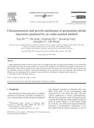
The morphology <strong>of</strong> the as-synthesized products<br />
was examined using SEM. A typical SEM image<br />
for ZnO <strong>nanowires</strong> is shown in Fig. 1(a). The<br />
image shows that large-scale ZnO <strong>nanowires</strong> were<br />
formed in high yield. The diameters <strong>of</strong> the<br />
<strong>nanowires</strong> range from 30 to 60 nm <strong>and</strong> <strong>their</strong><br />
lengths are up to several tens <strong>of</strong> micrometers.<br />
Bulk quantity <strong>of</strong> the products was analyzed by<br />
XRD. As shown in Fig. 1(b), the XRD pattern <strong>of</strong><br />
the ZnO <strong>nanowires</strong> can be indexed to a hexagonal<br />
structure <strong>of</strong> bulk ZnO with cell constants <strong>of</strong><br />
a0 ¼ 3:24 ( A <strong>and</strong> c0 ¼ 5:19 ( A. No diffraction peaks<br />
from Zn or other impurities have been found in<br />
our samples. Representative TEM images (Fig. 2)<br />
reveal the general morphology <strong>of</strong> the <strong>nanowires</strong>. It<br />
can be seen that the diameter <strong>of</strong> this ZnO nanowire<br />
is about 50 nm. It should be noted that a few<br />
nanoparticles do exist at the tip <strong>of</strong> the ZnO<br />
<strong>nanowires</strong> (Fig. 2(b)), as is indicated with arrowheads,<br />
<strong>and</strong> the diameters <strong>of</strong> these nanoparticles<br />
are about 2.0 times <strong>of</strong> that <strong>of</strong> the connected<br />
<strong>nanowires</strong>. Energy-dispersed X-ray spectrometry<br />
(EDX) analysis shows that the nanoparticles only<br />
contain Zn <strong>and</strong> Au. The same highly dispersed<br />
selected area electron diffraction (SAED) patterns<br />
[inset, Fig. 2(b)] taken from difference places along<br />
the axis <strong>of</strong> a single ZnO nanowire without tilting<br />
the specimen, show complete diffraction pattern,<br />
indicating that the ZnO <strong>nanowires</strong> are <strong>of</strong> single<br />
crystalline phase.<br />
There are two possible models for the <strong>growth</strong> <strong>of</strong><br />
conventional crystal whiskers or <strong>nanowires</strong>, the<br />
screw dislocation <strong>and</strong> vapor–liquid–solid (VLS). It<br />
is well known that the presence <strong>of</strong> a liquid drop is<br />
essential for the effective operation <strong>of</strong> the VLS<br />
mechanism. The solidified spherical droplets at the<br />
tips <strong>of</strong> the <strong>nanowires</strong> are commonly considered to<br />
be the evidence for the operation <strong>of</strong> the VLS<br />
mechanism, which is in agreement with our<br />
experimental conditions <strong>and</strong> the observed results<br />
(Fig. 2(b), indicated with arrowheads). The EDX<br />
analysis shows that these nanoparticles only<br />
contain Zn <strong>and</strong> Au. Why there is no atomic<br />
oxygen in the alloy drops at the tips <strong>of</strong> the<br />
<strong>nanowires</strong>? It is well known that the bonding<br />
energy <strong>of</strong> O2 is as high as 5.16 eV, which makes it
very difficult to decompose O2 into atomic oxygen<br />
at the conventional chemical vapor deposition<br />
(CVD) <strong>growth</strong> condition. Therefore, in this present<br />
case, O 2 cannot decompose into atomic<br />
oxygen at 9001C. The presence <strong>of</strong> a small amount<br />
<strong>of</strong> O2 is not expected to change the Au–Zn phase<br />
Y.W. Wang et al. / Journal <strong>of</strong> Crystal Growth 234 (2002) 171–175 173<br />
Fig. 1. The structure <strong>of</strong> ZnO <strong>nanowires</strong> (with wurtzite crystal structure). (a) Typical SEM image <strong>of</strong> the as-synthesized ZnO <strong>nanowires</strong><br />
obtained from thermal evaporation <strong>of</strong> Zn powders containing Au nanoparticles as catalyst at 9001C. (b) XRD pattern recorded from<br />
the ZnO <strong>nanowires</strong>.<br />
diagram, meanwhile they act as the oxygen source<br />
during the <strong>zinc</strong> <strong>oxide</strong> <strong>nanowires</strong> <strong>growth</strong>. Therefore,<br />
in this experimental process, the Zn vapor is<br />
rapidly generated at high temperature for the fast<br />
heating speed by vaporizing the <strong>zinc</strong> powders, <strong>and</strong><br />
reacted with the Au catalyst to form alloy droplets.
174<br />
Fig. 2. Typical TEM images showing the general morphology<br />
<strong>of</strong> ZnO <strong>nanowires</strong>: (a) a ultralong ZnO nanowire, (b) a thin<br />
ZnO nanowire with a Zn/Au alloy tip, (inset) the corresponding<br />
highly diffusive pattern <strong>of</strong> electron diffraction from the<br />
<strong>nanowires</strong>.<br />
As the droplets become supersaturated, ZnO<br />
<strong>nanowires</strong> are formed, by the reaction between<br />
Zn <strong>and</strong> O2.<br />
The room temperature PL <strong>of</strong> the ZnO <strong>nanowires</strong><br />
was examined <strong>and</strong> shown in Fig. 3. The<br />
excited wavelength was 380 nm <strong>and</strong> a 430 nm filter<br />
was used. The PL spectrum pattern has a strong<br />
green emission b<strong>and</strong> peaking around 520 nm. In<br />
the past several decades, the green luminescence<br />
mechanisms <strong>of</strong> ZnO have been studied, <strong>and</strong><br />
various models have been proposed [19,20].<br />
Vanheusden et al. [21] proved that the singly<br />
ionized oxygen vacancy is responsible for the green<br />
emission in the ZnO <strong>and</strong> the emission results from<br />
the recombination <strong>of</strong> a photogenerated hole with<br />
an electron occupying the oxygen vacancy. Huang<br />
et al. [17] have reported that the progressive<br />
increase <strong>of</strong> the green light emission intensity<br />
Y.W. Wang et al. / Journal <strong>of</strong> Crystal Growth 234 (2002) 171–175<br />
relative to the UV emission as the wire diameter<br />
decreases, which suggests that there is a great<br />
fraction <strong>of</strong> oxygen vacancies in the <strong>nanowires</strong>. We<br />
believe that <strong>nanowires</strong> with high ratios (length/<br />
diameter) should have more surface <strong>and</strong> subsurface<br />
oxygen vacancies. It was therefore reasonable<br />
to believe that the green light emission from<br />
the ZnO <strong>nanowires</strong> in our work could be<br />
attributed to the above-mentioned single ionized<br />
oxygen vacancy.<br />
4. Conclusions<br />
Fig. 3. PL spectrum <strong>of</strong> the ZnO <strong>nanowires</strong>.<br />
In summary, we have successfully synthesized<br />
ZnO <strong>nanowires</strong> in bulk quantities by simple<br />
physical evaporation. SEM <strong>and</strong> TEM observations<br />
show that the ZnO <strong>nanowires</strong> have diameters<br />
<strong>of</strong> about 30–60 nm <strong>and</strong> lengths up to several tens<br />
<strong>of</strong> micrometers. PL measurement taken on the<br />
bulk <strong>nanowires</strong> shows a green light emission,<br />
which was attributed to the single ionized oxygen<br />
vacancy formed in the <strong>nanowires</strong>. The availability<br />
<strong>of</strong> the ZnO <strong>nanowires</strong> is expected to enable<br />
fascinating opportunities such as probing confinement,<br />
dynamics <strong>and</strong> transport <strong>of</strong> excitons in one<br />
dimension, <strong>and</strong> creating optically active nanostructured<br />
materials.<br />
Acknowledgements<br />
This work was supported by National Major<br />
Project <strong>of</strong> Fundamental Research: Nanomaterials
<strong>and</strong> Nanostructures (Grant No. 19994506) <strong>and</strong> the<br />
Natural Science Foundation <strong>of</strong> China (Grant No.<br />
19974055).<br />
References<br />
[1] J.T. Hu, T.W. Odom, C.M. Lieber, Acc. Chem. Res. 32<br />
(1999) 435.<br />
[2] Y. Zhang, K. Suenaga, C. Colliex, S. Iijima, Science 281<br />
(1998) 973.<br />
[3] A.M. Morales, C.M. Lieber, Science 279 (1998) 208.<br />
[4] D.P. Yu, C.S. Lee, I. Bello, X.S. Sun, Y.H. Tang, G.W.<br />
Zhou, Z.G. Bai, Z. Zhang, S.Q. Feng, Solid State<br />
Commun. 105 (1998) 403.<br />
[5] C.R. Martin, Science 266 (1994) 1961.<br />
[6] Y. Li, Y. Ding, Z. Wang, Adv. Mater. 11 (1999) 844.<br />
[7] P. Yang, C.M. Lieber, Science 273 (1996) 1836.<br />
[8] J. Zhu, S. Fan, J. Mater. Res. 14 (1999) 1175.<br />
[9] M. Yazawa, M. Koguchi, A. Mute, M. Ozawa,<br />
K. Hiruma, Appl. Phys. Lett. 61 (1992) 2051.<br />
Y.W. Wang et al. / Journal <strong>of</strong> Crystal Growth 234 (2002) 171–175 175<br />
[10] P. Yang, C.M. Lieber, US Patent 5897945.<br />
[11] C.H. Liang, L.D. Zhang, G.W. Meng, Y.W. Wang, Z.Q.<br />
Chu, J. Non-Cryst. Solids 277 (2000) 63.<br />
[12] Z.G. Bai, D.P. Yu, H.Z. Zhang, Y. Ding, X.Z. Gai, Q.L.<br />
Hang, G.C. Xiong, S.Q. Feng, Chem. Phys. Lett. 303<br />
(1999) 311.<br />
[13] Y.C. Choi, W.S. Kim, Y.S. Park, S.M. Lee, D.J. Bae,<br />
Y.H. Lee, G.S. Park, W.B. Choi, N.S. Lee, J.M. Kim,<br />
Adv. Mater. 12 (2000) 746.<br />
[14] N. Riehl, H. Ortman, J. Electrochem. Soc. 60 (1956) 149.<br />
[15] S.D. Sharma, S.C. Kashyap, J. Appl. Phys. 42 (1971)<br />
5302.<br />
[16] Y. Li, G.W. Meng, L.D. Zhang, F. Phillipp, Appl. Phys.<br />
Lett. 76 (2000) 2011.<br />
[17] M.H. Huang, Y.Y. Wu, H.N. Feick, N. Tran, E. Weber,<br />
P.D. Yang, Adv. Mater. 13 (2001) 113.<br />
[18] S. Link, M.A. El-Sayed, J. Phys. Chem. B 103 (1999) 4212.<br />
[19] F.A. Kroger, H.J. Vink, J. Chem. Phys. 22 (1954) 250.<br />
[20] E.G. Byl<strong>and</strong>er, J. Appl. Phys. 49 (1978) 1188.<br />
[21] K. Vanheusden, W.L. Warren, C.H. Seager, D.K. Tallant,<br />
J.A. Voigt, B.E. Gnade, J. Appl. Phys. 79 (1996) 7983.