Single chip 433/868/915 MHz Transceiver nRF905 - Mobile Devices
Single chip 433/868/915 MHz Transceiver nRF905 - Mobile Devices
Single chip 433/868/915 MHz Transceiver nRF905 - Mobile Devices

You also want an ePaper? Increase the reach of your titles
YUMPU automatically turns print PDFs into web optimized ePapers that Google loves.
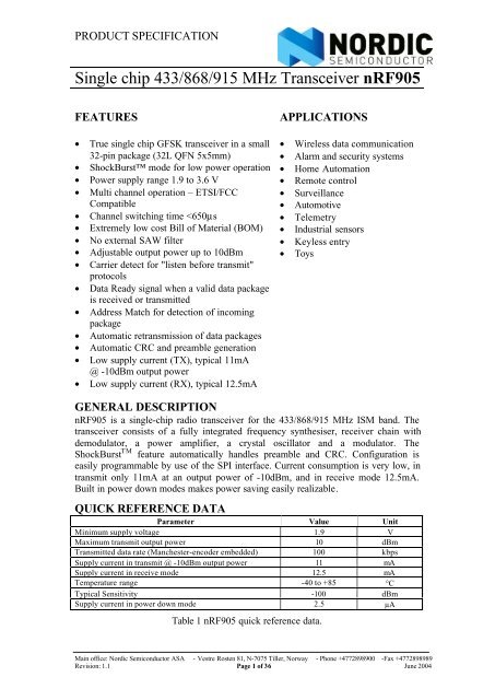
PRODUCT SPECIFICATION<br />
<strong>Single</strong> <strong>chip</strong> <strong>433</strong>/<strong>868</strong>/<strong>915</strong> <strong>MHz</strong> <strong>Transceiver</strong> <strong>nRF905</strong><br />
FEATURES APPLICATIONS<br />
• True single <strong>chip</strong> GFSK transceiver in a small<br />
32-pin package (32L QFN 5x5mm)<br />
• ShockBurst mode for low power operation<br />
• Power supply range 1.9 to 3.6 V<br />
• Multi channel operation – ETSI/FCC<br />
Compatible<br />
• Channel switching time
PRODUCT SPECIFICATION<br />
<strong>nRF905</strong> <strong>Single</strong> Chip <strong>433</strong>/<strong>868</strong>/<strong>915</strong> <strong>MHz</strong> Radio <strong>Transceiver</strong><br />
ORDERING INFORMATION<br />
Type Number Description Version<br />
<strong>nRF905</strong> IC 32L QFN 5x5mm -<br />
<strong>nRF905</strong>-EVKIT <strong>433</strong> Evaluation kit <strong>433</strong><strong>MHz</strong> 1.0<br />
<strong>nRF905</strong>-EVKIT <strong>868</strong>/<strong>915</strong> Evaluation kit <strong>868</strong>/<strong>915</strong><strong>MHz</strong> 1.0<br />
BLOCK DIAGRAM<br />
MISO (10)<br />
MOSI (11)<br />
SCK (12)<br />
CSN (13)<br />
TRX_CE (1)<br />
PWR_UP (2)<br />
TX_EN (32)<br />
CD (6)<br />
AM (7)<br />
DR (8)<br />
uPCLK (3)<br />
VSS (5)<br />
VSS (9)<br />
Table 2 <strong>nRF905</strong> ordering information.<br />
VSS (16)<br />
VSS (21)<br />
VSS (18)<br />
SPI<br />
interface<br />
TX - addr.<br />
TX - reg.<br />
RX - reg.<br />
Config-reg.<br />
ShockBurst<br />
Demod<br />
Dataslicer<br />
CRC code/<br />
decode<br />
Address<br />
decode<br />
GFSK<br />
filter<br />
Manchester<br />
encoder/<br />
decoder<br />
VSS (24)<br />
VSS (26)<br />
VSS (27)<br />
VSS (28)<br />
Voltage<br />
regulators<br />
IF BBF<br />
VSS (30)<br />
VSS (29)<br />
Crystal<br />
oscillator<br />
Main office: Nordic Semiconductor ASA - Vestre Rosten 81, N-7075 Tiller, Norway - Phone +4772898900 -Fax +4772898989<br />
Revision: 1.1 Page 2 of 36 June 2004<br />
VDD (4)<br />
VDD (25)<br />
VDD (17)<br />
LNA<br />
Frequency<br />
Synthesiser<br />
PA<br />
Figure 1 <strong>nRF905</strong> with external components.<br />
DVDD_1V2 (31)<br />
XC1 (14)<br />
XC2 (15)<br />
VDD_PA (19)<br />
ANT1 (20)<br />
ANT2 (21)<br />
IREF (23)
PRODUCT SPECIFICATION<br />
<strong>nRF905</strong> <strong>Single</strong> Chip <strong>433</strong>/<strong>868</strong>/<strong>915</strong> <strong>MHz</strong> Radio <strong>Transceiver</strong><br />
PIN FUNCTIONS<br />
Pin Name Pin function Description<br />
1 TRX_CE Digital input Enables <strong>chip</strong> for receive and transmit<br />
2 PWR_UP Digital input Power up <strong>chip</strong><br />
3 uPCLK Clock output Output clock, divided crystal oscillator full-swing clock<br />
4 VDD Power Power supply (+3V DC)<br />
5 VSS Power Ground (0V)<br />
6 CD Digital output Carrier Detect<br />
7 AM Digital output Address Match<br />
8 DR Digital output Receive and transmit Data Ready<br />
9 VSS Power Ground (0V)<br />
10 MISO SPI - interface SPI output<br />
11 MOSI SPI - interface SPI input<br />
12 SCK SPI - Clock SPI clock<br />
13 CSN SPI - enable SPI enable, active low<br />
14 XC1 Analog Input Crystal pin 1/ External clock reference pin<br />
15 XC2 Analog Output Crystal pin 2<br />
16 VSS Power Ground (0V)<br />
17 VDD Power Power supply (+3V DC)<br />
18 VSS Power Ground<br />
19 VDD_PA Power output Positive supply (1.8V) to <strong>nRF905</strong> power amplifier<br />
20 ANT1 RF Antenna interface 1<br />
21 ANT2 RF Antenna interface 2<br />
22 VSS Power Ground (0V)<br />
23 IREF Analog Input Reference current<br />
24 VSS Power Ground (0V)<br />
25 VDD Power Power supply (+3V DC)<br />
26 VSS Power Ground (0V)<br />
27 VSS Power Ground (0V)<br />
28 VSS Power Ground (0V)<br />
29 VSS Power Ground (0V)<br />
30 VSS Power Ground (0V)<br />
31 DVDD_1V2 Power Low voltage positive digital supply output for de-coupling<br />
32 TX_EN Digital input TX_EN=”1”TX mode, TX_EN=”0”RX mode<br />
Table 3 <strong>nRF905</strong> pin function.<br />
Main office: Nordic Semiconductor ASA - Vestre Rosten 81, N-7075 Tiller, Norway - Phone +4772898900 -Fax +4772898989<br />
Revision: 1.1 Page 3 of 36 June 2004
PRODUCT SPECIFICATION<br />
<strong>nRF905</strong> <strong>Single</strong> Chip <strong>433</strong>/<strong>868</strong>/<strong>915</strong> <strong>MHz</strong> Radio <strong>Transceiver</strong><br />
PIN ASSIGNMENT<br />
TRX_CE<br />
PWR_UP<br />
uPCLK<br />
VDD<br />
VSS<br />
CD<br />
AM<br />
DR<br />
1<br />
2<br />
3<br />
4<br />
5<br />
6<br />
7<br />
8<br />
TX_EN<br />
32<br />
VSS<br />
DVDD_1V2<br />
31<br />
<strong>nRF905</strong><br />
32L QFN 5x5<br />
MOSI<br />
VSS VSS VSS VSS VDD<br />
9 10 11 12 13 14 15 16<br />
MISO<br />
VSS<br />
30 29 28 27 26 25<br />
SCK<br />
XC2 VSS<br />
Figure 2 <strong>nRF905</strong> pin assignment (top view) for a 32L QFN 5x5 package.<br />
Main office: Nordic Semiconductor ASA - Vestre Rosten 81, N-7075 Tiller, Norway - Phone +4772898900 -Fax +4772898989<br />
Revision: 1.1 Page 4 of 36 June 2004<br />
CSN<br />
XC1<br />
24<br />
23<br />
22<br />
21<br />
20<br />
19<br />
18<br />
17<br />
VSS<br />
IREF<br />
VSS<br />
ANT2<br />
ANT1<br />
VDD_PA<br />
VSS<br />
VDD
PRODUCT SPECIFICATION<br />
<strong>nRF905</strong> <strong>Single</strong> Chip <strong>433</strong>/<strong>868</strong>/<strong>915</strong> <strong>MHz</strong> Radio <strong>Transceiver</strong><br />
ELECTRICAL SPECIFICATIONS<br />
Symbol Parameter (condition) Notes Min. Typ. Max. Units<br />
Operating conditions<br />
VDD Supply voltage 1.9 3.0 3.6 V<br />
TEMP Operating temperature -40 27 85 ºC<br />
Digital input pin<br />
V IH HIGH level input voltage VDD-0.3 VDD V<br />
V IL LOW level input voltage VSS 0.3 V<br />
Digital output pin<br />
V OH HIGH level output voltage (I OH=-0.5mA) VDD-0.3 VDD V<br />
V OL LOW level output voltage (I OL=0.5mA) VSS 0.3 V<br />
General electrical specification<br />
I stby_eclk Supply current in standby, uCLK enabled 1) 100 μA<br />
I stby_dclk Supply current in standby, uCLK disabled 2) 12.5 μA<br />
I PD Supply current in power down mode 2.5 μA<br />
I SPI Supply current in SPI programming 3) 20 μA<br />
General RF conditions<br />
f OP Operating frequency 4) 430 928 <strong>MHz</strong><br />
f XTAL Crystal frequency 5) 4 20 <strong>MHz</strong><br />
Δf Frequency deviation ±42 ±50 ±58 kHz<br />
R GFSK GFSK data rate, Manchester-encoded 100 kbps<br />
f CH<strong>433</strong> Channel spacing for <strong>433</strong><strong>MHz</strong> band 100 kHz<br />
f CH<strong>868</strong>/<strong>915</strong> Channel spacing for <strong>868</strong>/<strong>915</strong><strong>MHz</strong> band 200 kHz<br />
Transmitter operation<br />
P RF10 Output power 10dBm setting 6) 7 10 11 dBm<br />
P RF6 Output power 6dBm setting 6) 3 6 9 dBm<br />
P RF-2 Output power –2dBm setting 6) -6 -2 2 dBm<br />
P RF-10 Output power -10dBm setting 6) -14 -10 -6 dBm<br />
P BW 20dB bandwidth for modulated carrier 190 kHz<br />
P RF1 1 st adjacent channel transmit power 7) -27 dBc<br />
P RF2 2 nd adjacent channel transmit power 7) -54 dBc<br />
I TX10dBm Supply current @ 10dBm output power 30 mA<br />
I TX-10dBm Supply current @ -10dBm output power 11 mA<br />
Receiver operation<br />
I RX Supply current in receive mode 12.5 mA<br />
RX SENS Sensitivity at 0.1%BER -100 dBm<br />
RX MAX Maximum received signal 0 dBm<br />
C/I CO C/I Co-channel 8) 13 dB<br />
C/I 1ST 1 st adjacent channel selectivity C/I 200kHz 8) -7 dB<br />
C/I 2ND 2 nd adjacent channel selectivity C/I 400kHz 8) -16 dB<br />
C/I IM Image rejection 8) -30 dB<br />
Table 4 <strong>nRF905</strong> electrical specifications.<br />
1) Output frequency is 4<strong>MHz</strong> load of external clock pin is 5pF, Crystal is 4<strong>MHz</strong>.<br />
2) Crystal is 4<strong>MHz</strong>.<br />
3) Chip in power down, SPI_SCK frequency is 1<strong>MHz</strong>.<br />
4) Operates in the <strong>433</strong>, <strong>868</strong> and <strong>915</strong> <strong>MHz</strong> ISM band.<br />
5) The crystal frequency may be chosen from 5 different values (4, 8, 12, 16, and 20<strong>MHz</strong>)<br />
6) Optimum load impedance, please see peripheral RF information.<br />
7) Channel width and channel spacing is 200kHz.<br />
8) Channel Level +3dB over sensitivity, interfering signal a standard CW, image lies 2<strong>MHz</strong> above wanted.<br />
Main office: Nordic Semiconductor ASA - Vestre Rosten 81, N-7075 Tiller, Norway - Phone +4772898900 -Fax +4772898989<br />
Revision: 1.1 Page 5 of 36 June 2004
PRODUCT SPECIFICATION<br />
<strong>nRF905</strong> <strong>Single</strong> Chip <strong>433</strong>/<strong>868</strong>/<strong>915</strong> <strong>MHz</strong> Radio <strong>Transceiver</strong><br />
CURRENT CONSUMPTION<br />
MODE CRYSTAL<br />
FREQ. [MHZ]<br />
OUTPUT<br />
CLOCK<br />
FREQ. [MHZ]<br />
TYPICAL<br />
CURRENT<br />
Power Down 16 OFF 2.5 uA<br />
Standby 4 OFF 12 uA<br />
Standby 8 OFF 25 uA<br />
Standby 12 OFF 27 uA<br />
Standby 16 OFF 32 uA<br />
Standby 20 OFF 46 uA<br />
Standby 4 0.5 110 uA<br />
Standby 8 0.5 125 uA<br />
Standby 12 0.5 130 uA<br />
Standby 16 0.5 135 uA<br />
Standby 20 0.5 150 uA<br />
Standby 4 1 130 uA<br />
Standby 8 1 145 uA<br />
Standby 12 1 150 uA<br />
Standby 16 1 155 uA<br />
Standby 20 1 170 uA<br />
Standby 4 2 170 uA<br />
Standby 8 2 185 uA<br />
Standby 12 2 190 uA<br />
Standby 16 2 195 uA<br />
Standby 20 2 210 uA<br />
Standby 4 4 260 uA<br />
Standby 8 4 275 uA<br />
Standby 12 4 280 uA<br />
Standby 16 4 285 uA<br />
Standby 20 4 300 uA<br />
Rx @ <strong>433</strong> 16 OFF 12.2 mA<br />
Rx @ <strong>868</strong>/<strong>915</strong> 16 OFF 12.8 mA<br />
Reduced Rx 16 OFF 10.5 mA<br />
Tx @ 10dBm 16 OFF 30 mA<br />
Tx @ 6dBm 16 OFF 20 mA<br />
Tx @ -2dBm 16 OFF 14 mA<br />
Tx @ -10dBm 16 OFF 11 mA<br />
Conditions: VDD = 3.0V, VSS = 0V, TA = 27ºC,<br />
Load capacitance of external clock = 13pF, Crystal load capacitance = 12pF<br />
Table 5 <strong>nRF905</strong> current consumption.<br />
Main office: Nordic Semiconductor ASA - Vestre Rosten 81, N-7075 Tiller, Norway - Phone +4772898900 -Fax +4772898989<br />
Revision: 1.1 Page 6 of 36 June 2004
PRODUCT SPECIFICATION<br />
<strong>nRF905</strong> <strong>Single</strong> Chip <strong>433</strong>/<strong>868</strong>/<strong>915</strong> <strong>MHz</strong> Radio <strong>Transceiver</strong><br />
PACKAGE OUTLINE<br />
<strong>nRF905</strong> uses the QFN 32L 5x5 green package with a mat tin finish. Dimensions are in<br />
mm. Recommended soldering reflow profile can be found in application note<br />
nAN400-08, QFN soldering reflow guidelines, www.nordicsemi.no.<br />
+<br />
Package Type A A1 A2 b D E e J K L<br />
QFN32 Min 0.8 0.0 0.65 0.18<br />
3.2 3.2 0.3<br />
(5x5 mm) typ.<br />
0.23 5 BSC 5 BSC 0.5 BSC 3.3 3.3 0.4<br />
Max 0.9 0.05 0.69 0.3<br />
3.4 3.4 0.5<br />
Figure 3 <strong>nRF905</strong> package outline.<br />
Main office: Nordic Semiconductor ASA - Vestre Rosten 81, N-7075 Tiller, Norway - Phone +4772898900 -Fax +4772898989<br />
Revision: 1.1 Page 7 of 36 June 2004
PRODUCT SPECIFICATION<br />
<strong>nRF905</strong> <strong>Single</strong> Chip <strong>433</strong>/<strong>868</strong>/<strong>915</strong> <strong>MHz</strong> Radio <strong>Transceiver</strong><br />
ABSOLUTE MAXIMUM RATINGS<br />
Supply Voltages<br />
VDD...............................- 0.3V to + 3.6V<br />
VSS .....................................................0V<br />
Input Voltage<br />
VI..........................- 0.3V to VDD + 0.3V<br />
Output Voltage<br />
VO.........................- 0.3V to VDD + 0.3V<br />
Total Power Dissipation<br />
PD (TA=85°C)................................ 200mW<br />
Temperatures<br />
Operating temperature............................................ - 40°C to + 85°C<br />
Storage temperature...............................................- 40°C to + 125°C<br />
Note: Stress exceeding one or more of the limiting values may cause permanent<br />
damage to the device.<br />
ATTENTION!<br />
Electrostatic sensitive device.<br />
Observe precaution for handling.<br />
Main office: Nordic Semiconductor ASA - Vestre Rosten 81, N-7075 Tiller, Norway - Phone +4772898900 -Fax +4772898989<br />
Revision: 1.1 Page 8 of 36 June 2004
PRODUCT SPECIFICATION<br />
<strong>nRF905</strong> <strong>Single</strong> Chip <strong>433</strong>/<strong>868</strong>/<strong>915</strong> <strong>MHz</strong> Radio <strong>Transceiver</strong><br />
GLOSSARY OF TERMS<br />
Term Description<br />
ADC Analog to Digital Converter<br />
AM Address Match<br />
CD Carrier Detect<br />
CLK Clock<br />
CRC Cyclic Redundancy Check<br />
DR Data Ready<br />
GFSK Gaussian Frequency Shift Keying<br />
ISM Industrial-Scientific-Medical<br />
kSPS kilo Samples per Second<br />
MCU Micro Controller Unit<br />
PWR_DWN Power Down<br />
PWR_UP Power Up<br />
RX Receive<br />
SPI Serial Programmable Interface<br />
CSN SPI Chip Select Not<br />
MISO SPI Master In Slave Out<br />
MOSI SPI Master Out Slave In<br />
SCK SPI Serial Clock<br />
SPS Samples per Second<br />
STBY Standby<br />
TRX_EN Transmit/Receive Enable<br />
TX Transmit<br />
TX_EN Transmit Enable<br />
Table 6 Glossary of terms.<br />
Main office: Nordic Semiconductor ASA - Vestre Rosten 81, N-7075 Tiller, Norway - Phone +4772898900 -Fax +4772898989<br />
Revision: 1.1 Page 9 of 36 June 2004
PRODUCT SPECIFICATION<br />
<strong>nRF905</strong> <strong>Single</strong> Chip <strong>433</strong>/<strong>868</strong>/<strong>915</strong> <strong>MHz</strong> Radio <strong>Transceiver</strong><br />
MODES OF OPERATION<br />
The <strong>nRF905</strong> has two active (RX/TX) modes and two power-saving modes<br />
Active Modes<br />
• ShockBurst RX<br />
• ShockBurst TX<br />
Power Saving Modes<br />
• Power down and SPI - programming<br />
• Standby and SPI - programming<br />
The <strong>nRF905</strong> mode is decided by the settings of TRX_CE, TX_EN and PWR_UP.<br />
PWR_UP TRX_CE TX_EN Operating Mode<br />
0 X X Power down and SPI – programming<br />
1 0 X Standby and SPI – programming<br />
1 X 0 Read data from RX register<br />
1 1 0 Radio Enabled - ShockBurst TM RX<br />
1 1 1 Radio Enabled - ShockBurst TM TX<br />
nRF ShockBurst Mode<br />
Table 7 <strong>nRF905</strong> operational modes.<br />
The <strong>nRF905</strong> uses the Nordic Semiconductor ASA ShockBurst feature.<br />
ShockBurst TM makes it possible to use the high data rate offered by the <strong>nRF905</strong><br />
without the need of a costly, high-speed micro controller (MCU) for data<br />
processing/clock recovery. By placing all high speed signal processing related to RF<br />
protocol on-<strong>chip</strong>, the <strong>nRF905</strong> offers the application micro controller a simple SPI<br />
interface, the data rate is decided by the interface-speed the micro controller itself sets<br />
up. By allowing the digital part of the application to run at low speed, while<br />
maximizing the data rate on the RF link, the <strong>nRF905</strong> ShockBurst mode reduces the<br />
average current consumption in applications. In ShockBurst TM RX, Address Match<br />
(AM) and Data Ready (DR) notifies the MCU when a valid address and payload is<br />
received respectively. In ShockBurst TM TX, the <strong>nRF905</strong> automatically generates<br />
preamble and CRC. Data Ready (DR) notifies the MCU that the transmission is<br />
completed. All together, this means reduced memory demand in the MCU resulting in<br />
a low cost MCU, as well as reduced software development time.<br />
Main office: Nordic Semiconductor ASA - Vestre Rosten 81, N-7075 Tiller, Norway - Phone +4772898900 -Fax +4772898989<br />
Revision: 1.1 Page 10 of 36 June 2004
PRODUCT SPECIFICATION<br />
<strong>nRF905</strong> <strong>Single</strong> Chip <strong>433</strong>/<strong>868</strong>/<strong>915</strong> <strong>MHz</strong> Radio <strong>Transceiver</strong><br />
Typical ShockBurst TM TX:<br />
1. When the application MCU has data for a remote node, the address of the<br />
receiving node (TX-address) and payload data (TX-payload) are clocked<br />
into <strong>nRF905</strong> via the SPI interface. The application protocol or MCU sets<br />
the speed of the interface.<br />
2. MCU sets TRX_CE and TX_EN high, this activates a <strong>nRF905</strong><br />
ShockBurst transmission.<br />
3. <strong>nRF905</strong> ShockBurst:<br />
• Radio is automatically powered up.<br />
• Data package is completed (preamble added, CRC calculated).<br />
• Data package is transmitted (100kbps, GFSK, Manchester-encoded).<br />
• Data Ready is set high when transmission is completed.<br />
4. If AUTO_RETRAN is set high, the <strong>nRF905</strong> continuously retransmits the<br />
package until TRX_CE is set low.<br />
5. When TRX_CE is set low, the <strong>nRF905</strong> finishes transmitting the outgoing<br />
package and then sets itself into standby mode.<br />
The ShockBurst TM mode ensures that a transmitted package that has started always<br />
finishes regardless of what TRX_EN and TX_EN is set to during transmission. The<br />
new mode is activated when the transmission is completed. Please see subsequent<br />
chapters for detailed timing<br />
For test purposes such as antenna tuning and measuring output power it is possible to<br />
set the transmitter so that a constant carrier is produced. To do this TRX_CE must be<br />
maintained high instead of being pulsed. In addition Auto Retransmit should be<br />
switched off. After the burst of data has been sent then the device will continue to<br />
send the unmodulated carrier.<br />
Main office: Nordic Semiconductor ASA - Vestre Rosten 81, N-7075 Tiller, Norway - Phone +4772898900 -Fax +4772898989<br />
Revision: 1.1 Page 11 of 36 June 2004
PRODUCT SPECIFICATION<br />
<strong>nRF905</strong> <strong>Single</strong> Chip <strong>433</strong>/<strong>868</strong>/<strong>915</strong> <strong>MHz</strong> Radio <strong>Transceiver</strong><br />
SPI - programming<br />
uController loading ADDR<br />
and PAYLOAD data<br />
(Configuration register if<br />
changes since last TX/RX)<br />
YES<br />
Transmitter<br />
is powered<br />
up<br />
nRF ShockBurst TX<br />
NO<br />
Generate CRC and preamble<br />
Sending package<br />
DR is set high when completed<br />
NO<br />
Radio in Standby<br />
TX_EN = HI<br />
PWR_UP = HI<br />
TRX_CE = LO<br />
TRX_CE<br />
= HI ?<br />
TRX_CE<br />
= HI ?<br />
YES<br />
DR is<br />
set low<br />
after preamble<br />
NO<br />
Preamble<br />
AUTO_ YES<br />
RETRAN<br />
= HI ?<br />
Bit in configuration<br />
register<br />
Data Package<br />
ADDR PAYLOAD<br />
Figure 4 Flowchart ShockBurst TM transmit of <strong>nRF905</strong>.<br />
ADDR PAYLOAD CRC<br />
NB: DR is set low under the following conditions after it has been set high:<br />
• If TX_EN is set low<br />
• If PWR_UP is set low<br />
Main office: Nordic Semiconductor ASA - Vestre Rosten 81, N-7075 Tiller, Norway - Phone +4772898900 -Fax +4772898989<br />
Revision: 1.1 Page 12 of 36 June 2004
PRODUCT SPECIFICATION<br />
<strong>nRF905</strong> <strong>Single</strong> Chip <strong>433</strong>/<strong>868</strong>/<strong>915</strong> <strong>MHz</strong> Radio <strong>Transceiver</strong><br />
Typical ShockBurst TM RX:<br />
1. ShockBurst TM RX is selected by setting TRX_CE high and TX_EN low.<br />
2. After 650μs <strong>nRF905</strong> is monitoring the air for incoming communication.<br />
3. When the <strong>nRF905</strong> senses a carrier at the receiving frequency, Carrier<br />
Detect (CD) pin is set high.<br />
4. When a valid address is received, Address Match (AM) pin is set high.<br />
5. When a valid package has been received (correct CRC found), <strong>nRF905</strong><br />
removes the preamble, address and CRC bits, and the Data Ready (DR)<br />
pin is set high.<br />
6. MCU sets the TRX_CE low to enter standby mode (low current mode).<br />
7. MCU can clock out the payload data at a suitable rate via the SPI interface.<br />
8. When all payload data is retrieved, <strong>nRF905</strong> sets Data Ready (DR) and<br />
Address Match (AM) low again.<br />
9. The <strong>chip</strong> is now ready for entering ShockBurst TM RX, ShockBurst TM TX or<br />
power down mode.<br />
If TRX_CE or TX_EN is changed during an incoming package, the <strong>nRF905</strong> changes<br />
mode immediately and the package is lost. However, if the MCU is sensing the<br />
Address Match (AM) pin, it knows when the <strong>chip</strong> is receiving an incoming package<br />
and can therefore decide whether to wait for the Data Ready (DR) signal or enter a<br />
different mode.<br />
To avoid spurious address matches it is recommended that the address length be 24<br />
bits or higher in length. Small addresses such as 8 or 16 bits can often lead to<br />
statistical failures due to the address being repeated as part of the data packet. This<br />
can be avoided by using a longer address.<br />
Each byte within the address should be unique. Repeating bytes within the address<br />
reduces the effectiveness of the address and increases its susceptibility to noise hence<br />
increasing the packet error rate. The address should also have several level shifts (i.e.<br />
10101100) to reduce the statistical effect of noise and hence reduce the packet error<br />
rate.<br />
Main office: Nordic Semiconductor ASA - Vestre Rosten 81, N-7075 Tiller, Norway - Phone +4772898900 -Fax +4772898989<br />
Revision: 1.1 Page 13 of 36 June 2004
PRODUCT SPECIFICATION<br />
<strong>nRF905</strong> <strong>Single</strong> Chip <strong>433</strong>/<strong>868</strong>/<strong>915</strong> <strong>MHz</strong> Radio <strong>Transceiver</strong><br />
AM is set low<br />
YES<br />
Receiver is<br />
powered up<br />
NO<br />
Receiver<br />
Sensing for incomming data<br />
CD is set high if carrier<br />
NO<br />
NO<br />
Radio in Standby<br />
TX_EN = LO<br />
PWR_UP = HI<br />
TRX_CE<br />
= HI ?<br />
Correct<br />
ADDR?<br />
YES<br />
AM is set<br />
high<br />
Receiving<br />
data<br />
Correct<br />
CRC?<br />
YES<br />
DR high is<br />
set high<br />
TRX_CE<br />
= HI ?<br />
YES<br />
NO<br />
DR and AM are<br />
set low<br />
MCU clocks out payload via<br />
the SPI interface<br />
RX Remains<br />
On<br />
Data Package<br />
Preamble<br />
ADDR PAYLOAD CRC<br />
DR and AM are<br />
set low<br />
MCU clocks out payload via<br />
the SPI interface<br />
Radio enters<br />
STBY<br />
Figure 5 Flowchart ShockBurst TM receive of <strong>nRF905</strong>.<br />
PAYLOAD<br />
Main office: Nordic Semiconductor ASA - Vestre Rosten 81, N-7075 Tiller, Norway - Phone +4772898900 -Fax +4772898989<br />
Revision: 1.1 Page 14 of 36 June 2004
PRODUCT SPECIFICATION<br />
<strong>nRF905</strong> <strong>Single</strong> Chip <strong>433</strong>/<strong>868</strong>/<strong>915</strong> <strong>MHz</strong> Radio <strong>Transceiver</strong><br />
Power Down Mode<br />
In power down the <strong>nRF905</strong> is disabled with minimal current consumption, typically<br />
less than 2.5µA. When entering this mode the device is not active which will<br />
minimize average current consumption and maximizing battery lifetime. The<br />
configuration word content is maintained during power down.<br />
Standby Mode<br />
Standby mode is used to minimize average current consumption while maintaining<br />
short start up times to ShockBurst TM RX and ShockBurst TM TX. In this mode part of<br />
the crystal oscillator is active. Current consumption is dependent on crystal frequency,<br />
Ex: IDD= 12µA @4<strong>MHz</strong> and IDD =46μA @20<strong>MHz</strong>. If the uP-clock (pin 3) of <strong>nRF905</strong><br />
is enabled, current consumption increases and is dependent on the load capacitance<br />
and frequency. The configuration word content is maintained during standby.<br />
Main office: Nordic Semiconductor ASA - Vestre Rosten 81, N-7075 Tiller, Norway - Phone +4772898900 -Fax +4772898989<br />
Revision: 1.1 Page 15 of 36 June 2004
PRODUCT SPECIFICATION<br />
<strong>nRF905</strong> <strong>Single</strong> Chip <strong>433</strong>/<strong>868</strong>/<strong>915</strong> <strong>MHz</strong> Radio <strong>Transceiver</strong><br />
DEVICE CONFIGURATION<br />
All configuration of the <strong>nRF905</strong> is via the SPI interface. The interface consists of five<br />
registers; a SPI instruction set is used to decide which operation shall be performed.<br />
The SPI interface can be activated in any mode however Nordic Semiconductor ASA<br />
recommends the <strong>chip</strong> be in standby or power down mode.<br />
SPI Register Configuration<br />
The SPI interface consists of five internal registers. A register read-back mode is<br />
implemented to allow verification of the register contents.<br />
MISO<br />
MOSI<br />
SCK<br />
CSN<br />
Status – Register<br />
I/O-reg<br />
TX-PAYLOAD<br />
Main office: Nordic Semiconductor ASA - Vestre Rosten 81, N-7075 Tiller, Norway - Phone +4772898900 -Fax +4772898989<br />
Revision: 1.1 Page 16 of 36 June 2004<br />
EN<br />
DTA<br />
CLK<br />
EN<br />
DTA<br />
CLK<br />
EN<br />
DTA<br />
CLK<br />
EN<br />
DTA<br />
CLK<br />
EN<br />
DTA<br />
CLK<br />
STATUS-REGISTER<br />
RF - CONFIGURATION<br />
REGISTER<br />
TX-ADDRESS<br />
RX-PAYLOAD<br />
Figure 6 SPI – interface and the five internal registers.<br />
Register contains status of Data Ready (DR) and Address Match (AM).<br />
RF - Configuration Register<br />
Register contains transceiver setup information such as frequency and output power<br />
ext.<br />
TX – Address<br />
Register contains address of target device. How many bytes used is set in the<br />
configuration register.<br />
TX – Payload<br />
Register containing the payload information to be sent in a ShockBurst TM package.<br />
How many bytes used is set in the configuration register.<br />
RX – Payload<br />
Register containing the payload information derived from a received valid ShockBurst<br />
TM package. How many bytes used is set in the configuration register. Valid data in<br />
the RX-Payload register is indicated with a high Date Ready (DR) signal.
PRODUCT SPECIFICATION<br />
<strong>nRF905</strong> <strong>Single</strong> Chip <strong>433</strong>/<strong>868</strong>/<strong>915</strong> <strong>MHz</strong> Radio <strong>Transceiver</strong><br />
SPI Instruction Set<br />
The available commands to be used on the SPI interface is shown below. Whenever<br />
CSN is set low the interface expects an instruction. Every new instruction must be<br />
started by a high to low transition on CSN.<br />
Instruction set for the <strong>nRF905</strong> SPI Serial Interface<br />
Instruction Name Instruction<br />
Format<br />
Operation<br />
W_CONFIG<br />
0000 AAAA Write Configuration-register. AAAA indicates which byte<br />
(WC)<br />
the write operation is to be started from. Number of bytes<br />
depends on start address AAAA.<br />
R_CONFIG<br />
0001 AAAA Read Configuration-register. AAAA indicates which byte<br />
(RC)<br />
the read operation is to be started from. Number of bytes<br />
depends on start address AAAA.<br />
W_TX_PAYLOAD 0010 0000 Write TX-payload: 1 – 32 bytes. A write operation will<br />
(WTP)<br />
always start at byte 0.<br />
R_TX_PAYLOAD 0010 0001 Read TX-payload: 1 – 32 bytes. A read operation will<br />
(RTP)<br />
always start at byte 0.<br />
W_TX_ADDRESS 0010 0010 Write TX-address: 1 – 4 bytes. A write operation will<br />
(WTA)<br />
always start at byte 0.<br />
R_TX_ADDRESS 0010 0011 Read TX-address: 1 – 4 bytes. A read operation will<br />
(RTA)<br />
always start at byte 0<br />
R_RX_PAYLOAD 0010 0100 Read RX-payload: 1 – 32 bytes. A read operation will<br />
(RRP)<br />
always start at byte 0.<br />
CHANNEL_CONFIG 1000 pphc Special command for fast setting of CH_NO,<br />
(CC)<br />
cccc cccc HFREQ_PLL and PA_PWR in the CONFIGURATION<br />
REGISTER. CH_NO= ccccccccc, HFREQ_PLL = h<br />
PA_PWR = pp<br />
Table 8 Instruction set for the <strong>nRF905</strong> SPI interface.<br />
A read or a write operation may operate on a single byte or on a set of succeeding<br />
bytes from a given start address defined by the instruction. When accessing<br />
succeeding bytes one will read or write MSB of the byte with the smallest byte<br />
number first. The content of the status-register will always be read to MISO after a<br />
high to low transition on CSN.<br />
Main office: Nordic Semiconductor ASA - Vestre Rosten 81, N-7075 Tiller, Norway - Phone +4772898900 -Fax +4772898989<br />
Revision: 1.1 Page 17 of 36 June 2004
PRODUCT SPECIFICATION<br />
<strong>nRF905</strong> <strong>Single</strong> Chip <strong>433</strong>/<strong>868</strong>/<strong>915</strong> <strong>MHz</strong> Radio <strong>Transceiver</strong><br />
SPI Timing<br />
Data is clocked into or out of the device on the rising edge of the clock pulse. The<br />
clock speed is determined by the MCU and may be from 1Hz to 10<strong>MHz</strong> depending on<br />
the MCU. The device must be in one of the power saving modes for the configuration<br />
registers to be read or written to.<br />
CSN<br />
SCK<br />
MOSI<br />
MISO<br />
CSN<br />
SCK<br />
MOSI<br />
MISO<br />
C<br />
7<br />
0 1 2 3 7 8 15<br />
Command 8 bits, MSB = C7<br />
C<br />
6<br />
C<br />
5<br />
C<br />
4<br />
C<br />
3<br />
C<br />
2<br />
C<br />
1<br />
C<br />
0<br />
Status byte as output, MSB = S7 Addressed byte as output, MSB = O7<br />
S<br />
7<br />
C<br />
7<br />
S<br />
6<br />
S<br />
5<br />
S<br />
4<br />
S<br />
3<br />
S<br />
2<br />
S<br />
1<br />
S<br />
0<br />
O<br />
7<br />
O<br />
6<br />
O<br />
5<br />
O<br />
4<br />
O<br />
3<br />
Succeeding bytes to addressed byte<br />
as output<br />
Main office: Nordic Semiconductor ASA - Vestre Rosten 81, N-7075 Tiller, Norway - Phone +4772898900 -Fax +4772898989<br />
Revision: 1.1 Page 18 of 36 June 2004<br />
O<br />
2<br />
O<br />
1<br />
O<br />
0<br />
Figure 7 SPI read operation.<br />
0 1 2 3 7 8 15<br />
Command 8 bits, MSB = C7<br />
C<br />
6<br />
C<br />
5<br />
C<br />
4<br />
C<br />
3<br />
C<br />
2<br />
Status byte as output, MSB = S7<br />
S<br />
7<br />
S<br />
6<br />
S<br />
5<br />
S<br />
4<br />
S<br />
3<br />
S<br />
2<br />
C<br />
1<br />
S<br />
1<br />
C<br />
0<br />
S<br />
0<br />
D<br />
7<br />
First data byte as input, MSB = D7<br />
D<br />
6<br />
D<br />
5<br />
D<br />
4<br />
Figure 8 SPI write operation.<br />
D<br />
3<br />
D<br />
2<br />
D<br />
1<br />
D<br />
0<br />
Succeeding data bytes as input
PRODUCT SPECIFICATION<br />
<strong>nRF905</strong> <strong>Single</strong> Chip <strong>433</strong>/<strong>868</strong>/<strong>915</strong> <strong>MHz</strong> Radio <strong>Transceiver</strong><br />
RF - Configuration – Register Description<br />
Parameter Bitwidth Description<br />
CH_NO 9 Sets center freq. together with HFREQ_PLL (default = 001101100 b = 108 d).<br />
HFREQ_<br />
PLL<br />
f RF = ( 422.4 + CH_NO d /10)*(1+HFREQ_PLL d) <strong>MHz</strong><br />
1 Sets PLL in <strong>433</strong> or <strong>868</strong>/<strong>915</strong> <strong>MHz</strong> mode (default = 0).<br />
'0' – Chip operating in <strong>433</strong><strong>MHz</strong> band<br />
'1' – Chip operating in <strong>868</strong> or <strong>915</strong> <strong>MHz</strong> band<br />
PA_PWR 2 Output power (default = 00).<br />
'00' -10dBm<br />
'01' -2dBm<br />
'10' +6dBm<br />
'11' +10dBm<br />
RX_RED_<br />
PWR<br />
AUTO_<br />
RETRAN<br />
1 Reduces current in RX mode by 1.6mA. Sensitivity is reduced (default = 0).<br />
'0' – Normal operation<br />
'1' – Reduced power<br />
1 Retransmit contents in TX register if TRX_CE and TXEN are high (default = 0).<br />
'0' – No retransmission<br />
'1' – Retransmission of data package<br />
RX_AFW 3 RX-address width (default = 100).<br />
'001' – 1 byte RX address field width<br />
'100' – 4 byte RX address field width<br />
TX_AFW 3 TX-address width (default = 100).<br />
'001' – 1 byte TX address field width<br />
'100' – 4 byte TX address field width<br />
RX_PW 6 RX-payload width (default = 100000).<br />
'000001' – 1 byte RX payload field width<br />
'000010' – 2 byte RX payload field width<br />
.<br />
'100000' – 32 byte RX payload field width<br />
TX_PW 6 TX-payload width (default = 100000).<br />
'000001' – 1 byte TX payload field width<br />
'000010' – 2 byte TX payload field width<br />
.<br />
'100000' – 32 byte TX payload field width<br />
RX_<br />
ADDRESS<br />
32 RX address identity. Used bytes depend on RX_AFW (default = E7E7E7E7h). UP_CLK_<br />
FREQ<br />
UP_CLK_<br />
EN<br />
2 Output clock frequency (default = 11).<br />
'00' – 4<strong>MHz</strong><br />
'01' – 2<strong>MHz</strong><br />
'10' – 1<strong>MHz</strong><br />
'11' – 500kHz<br />
1 Output clock enable (default = 1).<br />
'0' – No external clock signal available<br />
'1' – External clock signal enabled<br />
XOF 3 Crystal oscillator frequency. Must be set according to external crystal resonantfrequency<br />
(default = 100).<br />
'000' – 4<strong>MHz</strong><br />
'001' – 8<strong>MHz</strong><br />
'010' – 12<strong>MHz</strong><br />
'011' – 16<strong>MHz</strong><br />
'100' – 20<strong>MHz</strong><br />
CRC_EN 1 CRC – check enable (default = 1).<br />
'0' – Disable<br />
CRC_<br />
MODE<br />
'1' – Enable<br />
1 CRC – mode (default = 1).<br />
'0' – 8 CRC check bit<br />
'1' – 16 CRC check bit<br />
Table 9 Configuration-register description.<br />
Main office: Nordic Semiconductor ASA - Vestre Rosten 81, N-7075 Tiller, Norway - Phone +4772898900 -Fax +4772898989<br />
Revision: 1.1 Page 19 of 36 June 2004
PRODUCT SPECIFICATION<br />
<strong>nRF905</strong> <strong>Single</strong> Chip <strong>433</strong>/<strong>868</strong>/<strong>915</strong> <strong>MHz</strong> Radio <strong>Transceiver</strong><br />
Register Contents<br />
Byte #<br />
RF-CONFIG_REGISTER (R/W)<br />
Content bit[7:0], MSB = bit[7] Init value<br />
0 CH_NO[7:0] 0110_1100<br />
1 bit[7:6] not used, AUTO_RETRAN, RX_RED_PWR, PA_PWR[1:0], 0000_0000<br />
HFREQ_PLL, CH_NO[8]<br />
2 bit[7] not used, TX_AFW[2:0] , bit[3] not used, RX_AFW[2:0] 0100_0100<br />
3 bit[7:6] not used, RX_PW[5:0] 0010_0000<br />
4 bit[7:6] not used, TX_PW[5:0] 0010_0000<br />
5 RX_ADDRESS (device identity) byte 0 E7<br />
6 RX_ADDRESS (device identity) byte 1 E7<br />
7 RX_ADDRESS (device identity) byte 2 E7<br />
8 RX_ADDRESS (device identity) byte 3 E7<br />
9 CRC_MODE,CRC_EN, XOF[2:0], UP_CLK_EN, UP_CLK_FREQ[1:0] 1110_0111<br />
TX_PAYLOAD (R/W)<br />
Byte # Content bit[7:0], MSB = bit[7] Init value<br />
0 TX_PAYLOAD[7:0] X<br />
1 TX_PAYLOAD[15:8] X<br />
- - X<br />
- - X<br />
30 TX_PAYLOAD[247:240] X<br />
31 TX_PAYLOAD[255:248] X<br />
TX_ADDRESS (R/W)<br />
Byte # Content bit[7:0], MSB = bit[7] Init value<br />
0 TX_ADDRESS[7:0] E7<br />
1 TX_ADDRESS[15:8] E7<br />
2 TX_ADDRESS[23:16] E7<br />
3 TX_ADDRESS[31:24] E7<br />
RX_PAYLOAD (R)<br />
Byte # Content bit[7:0], MSB = bit[7] Init value<br />
0 RX_PAYLOAD[7:0] X<br />
1 RX_PAYLOAD[15:8] X<br />
- X<br />
- X<br />
30 RX_PAYLOAD[247:240] X<br />
31 RX_PAYLOAD[255:248] X<br />
STATUS_REGISTER (R)<br />
Byte # Content bit[7:0], MSB = bit[7] Init value<br />
0 AM, bit [6] not used, DR, bit [0:4] not used X<br />
Table 10 RF register contents.<br />
The length of all registers is fixed. However, the bytes in TX_PAYLOAD,<br />
RX_PAYLOAD, TX_ADDRESS and RX_ADDRESS used in ShockBurst TM RX/TX<br />
are set in the configuration register. Register content is not lost when the device enters<br />
one of the power saving modes.<br />
Main office: Nordic Semiconductor ASA - Vestre Rosten 81, N-7075 Tiller, Norway - Phone +4772898900 -Fax +4772898989<br />
Revision: 1.1 Page 20 of 36 June 2004
PRODUCT SPECIFICATION<br />
<strong>nRF905</strong> <strong>Single</strong> Chip <strong>433</strong>/<strong>868</strong>/<strong>915</strong> <strong>MHz</strong> Radio <strong>Transceiver</strong><br />
IMPORTANT TIMING DATA<br />
The following timing must be obeyed during <strong>nRF905</strong> operation.<br />
Device Switching Times<br />
<strong>nRF905</strong> timing Max.<br />
PWR_DWN ST_BY mode 3 ms<br />
STBY TX Shock Burst 650 μs<br />
STBY RX Shock Burst 650 μs<br />
RX Shock Burst TX Shock Burst 550 1 μs<br />
TX Shock Burst RX Shock Burst 550 1 μs<br />
Notes to table:<br />
1) RX to TX or TX to RX switching is available without re-programming of the RF<br />
configuration register. The same frequency channel is maintained.<br />
ShockBurst TM TX timing<br />
MOSI<br />
CSN<br />
PWR_UP<br />
TX_EN<br />
TRX_CE<br />
TX DATA<br />
TIME<br />
Table 11 Switching times for <strong>nRF905</strong>.<br />
Programming of<br />
Configuration Register<br />
and TX Data Register<br />
T0 = Radio Enabled<br />
T1 = T0+10uS Minimum TRX_CE pulse<br />
T2 = T0 + 650uS.Start of TX Data transmission<br />
T3 = End of Data Packet, enter Standby mode<br />
T0 T1 T2 T3<br />
Transmitted Data 100kbps<br />
Manchester Encoded<br />
Figure 9 Timing diagram for standby to transmit.<br />
After a data packet has finished transmitting the device will automatically enter<br />
Standby mode and wait for the next pulse of TRX_CE. If the Auto Re-Transmit<br />
function is enabled the data packet will continue re-sending the same data packet until<br />
TRX_CE is set low.<br />
Main office: Nordic Semiconductor ASA - Vestre Rosten 81, N-7075 Tiller, Norway - Phone +4772898900 -Fax +4772898989<br />
Revision: 1.1 Page 21 of 36 June 2004
PRODUCT SPECIFICATION<br />
<strong>nRF905</strong> <strong>Single</strong> Chip <strong>433</strong>/<strong>868</strong>/<strong>915</strong> <strong>MHz</strong> Radio <strong>Transceiver</strong><br />
ShockBurst TM RX timing<br />
PWR_UP<br />
TX_EN<br />
TRX_CE<br />
RX DATA<br />
TIME<br />
CD<br />
AM<br />
DR<br />
650uS<br />
650uS to enter RX<br />
mode from<br />
TRX_CE being set<br />
high.<br />
T0 T1 T2 T3<br />
T0 = Receiver Enabled -Listening for Data<br />
T1 = Carrier Detect finds a carrier<br />
T2 = AM - Correct Address Found<br />
T3 = DR - Data packet with correct Address/CRC<br />
Figure 10 Timing diagram for standby to receiving.<br />
After the Data Ready (DR) has been set high a valid data packet is available in the RX<br />
data register. This may be clocked out in RX mode or standby mode. After the data<br />
has been clocked out via the SPI interface the Data Ready (DR) and Address Match<br />
(AM) pins are reset to low.<br />
The RX register is reset if the PWR_UP pin is taken low or if the device is switched<br />
into TX mode i.e. TXEN is taken high. This will also results in the Data Ready(DR)<br />
and Address Match (AM) pins being reset to low.<br />
Main office: Nordic Semiconductor ASA - Vestre Rosten 81, N-7075 Tiller, Norway - Phone +4772898900 -Fax +4772898989<br />
Revision: 1.1 Page 22 of 36 June 2004
PRODUCT SPECIFICATION<br />
<strong>nRF905</strong> <strong>Single</strong> Chip <strong>433</strong>/<strong>868</strong>/<strong>915</strong> <strong>MHz</strong> Radio <strong>Transceiver</strong><br />
PERIPHERAL RF INFORMATION<br />
Crystal Specification<br />
Tolerance includes initially accuracy and tolerance over temperature and aging.<br />
Frequency CL ESR C0max Tolerance @ Tolerance @<br />
<strong>868</strong>/<strong>915</strong> <strong>MHz</strong> <strong>433</strong> <strong>MHz</strong><br />
4<strong>MHz</strong> 12pF 150Ω 7.0pF ±30ppm ±60ppm<br />
8<strong>MHz</strong> 12pF 100Ω 7.0pF ±30ppm ±60ppm<br />
12<strong>MHz</strong> 12pF 100Ω 7.0pF ±30ppm ±60ppm<br />
16<strong>MHz</strong> 12pF 100Ω 7.0pF ±30ppm ±60ppm<br />
20<strong>MHz</strong> 12pF 100Ω 7.0pF ±30ppm ±60ppm<br />
Table 12 Crystal specification of <strong>nRF905</strong>.<br />
To achieve a crystal oscillator solution with low power consumption and fast start-up<br />
time, it is recommended to specify the crystal with a low value of crystal load<br />
capacitance. Specifying CL =12pF is acceptable, but it is possible to use up to 16pF.<br />
Specifying a lower value of crystal parallel equivalent capacitance, Co=1.5pF is also<br />
good, but this can increase the price of the crystal itself. Typically Co=1.5pF at a<br />
crystal specified for Co_max=7.0pF.<br />
External Clock Reference<br />
An external reference clock, such as a MCU clock, may be used instead of a crystal.<br />
The clock signal should be applied directly to the XC1 pin, the XC2 pin can be left<br />
high impedance. When operating with an external clock instead of a crystal the clock<br />
must be applied in standby mode to achieve low current consumption. If the device is<br />
set into standby mode with no external clock or crystal then the current consumption<br />
will increase up to a maximum of 1mA.<br />
Microprocessor Output Clock<br />
By default a microprocessor clock output is provided. Providing an output clock will<br />
increase the current consumption in standby mode. The current consumption in<br />
standby will depend on frequency and load of external crystal, frequency of output<br />
clock and capacitive load of the provided output clock. Typical current consumption<br />
values are found in Table 5<br />
Main office: Nordic Semiconductor ASA - Vestre Rosten 81, N-7075 Tiller, Norway - Phone +4772898900 -Fax +4772898989<br />
Revision: 1.1 Page 23 of 36 June 2004
PRODUCT SPECIFICATION<br />
<strong>nRF905</strong> <strong>Single</strong> Chip <strong>433</strong>/<strong>868</strong>/<strong>915</strong> <strong>MHz</strong> Radio <strong>Transceiver</strong><br />
Antenna Output<br />
The “ANT1 & ANT2” output pins provide a balanced RF output to the antenna. The<br />
pins must have a DC path to VDD_PA, either via a RF choke or via the center point<br />
in a dipole antenna. The load impedance seen between the ANT1/ANT2 outputs<br />
should be in the range 200-700Ω. The optimum differential load impedance at the<br />
antenna ports is given as:<br />
900<strong>MHz</strong> 225Ω+j210<br />
430<strong>MHz</strong> 300Ω+j100<br />
A low load impedance (for instance 50Ω) can be obtained by fitting a simple<br />
matching network or a RF transformer (balun). Further information regarding balun<br />
structures and matching networks may be found in the Application Examples chapter.<br />
Output Power Adjustment<br />
The power amplifier in <strong>nRF905</strong> can be programmed to four different output power<br />
settings by the configuration register. By reducing output power, the total TX current<br />
is reduced.<br />
Power setting RF output power DC current consumption<br />
00 -10 dBm 11.0 mA<br />
01 -2 dBm 14.0 mA<br />
10 6 dBm 20.0 mA<br />
11 10 dBm 30.0 mA<br />
Conditions: VDD = 3.0V, VSS = 0V, TA = 27ºC, Load impedance = 400 Ω.<br />
Table 13 RF output power setting for the <strong>nRF905</strong>.<br />
Modulation<br />
The modulation of <strong>nRF905</strong> is Gaussian Frequency Shift Keying (GFSK) with a datarate<br />
of 100kbps. Deviation is ±50kHz. GFSK modulation results in a more bandwidth<br />
effective transmission-link compared with ordinary FSK modulation.<br />
The data is internally Manchester encoded (TX) and Manchester decoded (RX). That<br />
is, the effective symbol-rate of the link is 50kbps. By using internally Manchester<br />
encoding, no scrambling in the u-controller is needed.<br />
Main office: Nordic Semiconductor ASA - Vestre Rosten 81, N-7075 Tiller, Norway - Phone +4772898900 -Fax +4772898989<br />
Revision: 1.1 Page 24 of 36 June 2004
PRODUCT SPECIFICATION<br />
<strong>nRF905</strong> <strong>Single</strong> Chip <strong>433</strong>/<strong>868</strong>/<strong>915</strong> <strong>MHz</strong> Radio <strong>Transceiver</strong><br />
Output Frequency<br />
The operating RF-frequency of <strong>nRF905</strong> is set in the configuration register by CH_NO<br />
and HFREQ_PLL. The operating frequency is given by:<br />
f OP<br />
= ( 422.<br />
4 + ( CH _ NO/<br />
10))<br />
⋅ ( 1+<br />
HFREQ _ PLL)<br />
<strong>MHz</strong><br />
When HFREQ_PLL is ‘0’ the frequency resolution is 100kHz and when it is ‘1’ the<br />
resolution is 200kHz.<br />
The application operating frequency has to be chosen to apply with the Short Range<br />
Devise regulation in the area of operation.<br />
Operating frequency HFREQ_PLL CH_NO<br />
430.0 <strong>MHz</strong> [0] [001001100]<br />
<strong>433</strong>.1 <strong>MHz</strong> [0] [001101011]<br />
<strong>433</strong>.2 <strong>MHz</strong> [0] [001101100]<br />
434.7 <strong>MHz</strong> [0] [001111011]<br />
862.0 <strong>MHz</strong> [1] [001010110]<br />
<strong>868</strong>.2 <strong>MHz</strong> [1] [001110101]<br />
<strong>868</strong>.4 <strong>MHz</strong> [1] [001110110]<br />
869.8 <strong>MHz</strong> [1] [001111101]<br />
902.2 <strong>MHz</strong> [1] [100011111]<br />
902.4 <strong>MHz</strong> [1] [100100000]<br />
927.8 <strong>MHz</strong> [1] [110011111]<br />
Table 14 Examples of real operating frequencies.<br />
Main office: Nordic Semiconductor ASA - Vestre Rosten 81, N-7075 Tiller, Norway - Phone +4772898900 -Fax +4772898989<br />
Revision: 1.1 Page 25 of 36 June 2004
PRODUCT SPECIFICATION<br />
<strong>nRF905</strong> <strong>Single</strong> Chip <strong>433</strong>/<strong>868</strong>/<strong>915</strong> <strong>MHz</strong> Radio <strong>Transceiver</strong><br />
PCB Layout and Decoupling Guidelines<br />
<strong>nRF905</strong> is an extremely robust RF device due to internal voltage regulators and<br />
requires the minimum of RF layout protocols. However the following design rules<br />
should still be incorporated into the layout design.<br />
A PCB with a minimum of two layers including a ground plane is recommended for<br />
optimum performance. The <strong>nRF905</strong> DC supply voltage should be decoupled as close<br />
as possible to the VDD pins with high performance RF capacitors. It is preferable to<br />
mount a large surface mount capacitor (e.g. 4.7μF tantalum) in parallel with the<br />
smaller value capacitors. The <strong>nRF905</strong> supply voltage should be filtered and routed<br />
separately from the supply voltages of any digital circuitry.<br />
Long power supply lines on the PCB should be avoided. All device grounds, VDD<br />
connections and VDD bypass capacitors must be connected as close as possible to the<br />
<strong>nRF905</strong> IC. For a PCB with a topside RF ground plane, the VSS pins should be<br />
connected directly to the ground plane. For a PCB with a bottom ground plane, the<br />
best technique is to place via holes as close as possible to the VSS pins. A minimum<br />
of one via hole should be used for each VSS pin.<br />
Full swing digital data or control signals should not be routed close to the crystal or<br />
the power supply lines.<br />
A fully qualified RF-layout for the <strong>nRF905</strong> and its surrounding components,<br />
including antennas and matching networks, can be downloaded from<br />
www.nordicsemi.no.<br />
Main office: Nordic Semiconductor ASA - Vestre Rosten 81, N-7075 Tiller, Norway - Phone +4772898900 -Fax +4772898989<br />
Revision: 1.1 Page 26 of 36 June 2004
PRODUCT SPECIFICATION<br />
<strong>nRF905</strong> <strong>Single</strong> Chip <strong>433</strong>/<strong>868</strong>/<strong>915</strong> <strong>MHz</strong> Radio <strong>Transceiver</strong><br />
<strong>nRF905</strong> FEATURES<br />
Carrier Detect.<br />
When the <strong>nRF905</strong> is in ShockBurst TM RX, the Carrier Detect (CD) pin is set high if a<br />
RF carrier is present at the channel the device is programmed to. This feature is very<br />
effective to avoid collision of packages from different transmitters operating at the<br />
same frequency. Whenever a device is ready to transmit it could first be set into<br />
receive mode and sense whether or not the wanted channel is available for outgoing<br />
data. This forms a very simple listen before transmit protocol. Operating Carrier<br />
Detect (CD) with Reduced RX Power mode is an extremely power efficient RF<br />
system. Typical Carrier Detect level (CD) is typically 5dB lower than sensitivity, i.e.<br />
if sensitivity is –100dBm then the Carrier Detect function will sense a carrier wave as<br />
low as –105dBm. Below –105dBm the Carrier Detect signal will be low, i.e. 0V.<br />
Above –95dBm the Carrier Detect signal will be high, i.e. Vdd. Between<br />
approximately -95 to -105 the Carrier Detect Signal will toggle.<br />
Address Match<br />
When the <strong>nRF905</strong> is in ShockBurst TM RX mode, the Address Match (AM) pin is set<br />
high as soon as an incoming package with an address that is identical with the<br />
device’s own identity is received. With the Address Match pin the controller is alerted<br />
that the <strong>nRF905</strong> is receiving data actually before the Data Ready (DR) signal is set<br />
high. If the Data Ready (DR) pin is not set high i.e. the CRC is incorrect then the<br />
Address Match (AM) pin is reset to low at the end of the received data packet. This<br />
function can be very useful for an MCU. If Address Match (AM) is high then the<br />
MCU can make a decision to wait and see if Data Ready (DR) will be set high<br />
indicating a valid data package has been received or ignore that a possible package is<br />
being received and switch modes.<br />
Data Ready<br />
The Data Ready (DR) signal makes it possible to largely reduce the complexity of the<br />
MCU software program.<br />
In ShockBurst TM TX, the Data Ready (DR) signal is set high when a complete<br />
package is transmitted, telling the MCU that the <strong>nRF905</strong> is ready for new actions. It is<br />
reset to low at the start of a new package transmission or when switched to a different<br />
mode i.e. receive mode or standby mode.<br />
In ShockBurst TM TX Auto Retransmit the Data Ready (DR) signal is set high at the<br />
beginning of the pre-amble and is set low at the end of the preamble. The Data Ready<br />
(DR) signal therefore pulses at the beginning of each transmitted data packet.<br />
In ShockBurst TM RX, the signal is set high when <strong>nRF905</strong> has received a valid<br />
package, i.e. a valid address, package length and correct CRC. The MCU can then<br />
retrieve the payload via the SPI interface. The Data Ready (DR) pin is reset to low<br />
once the data has been clocked out of the data buffer or the device is switched to<br />
transmit mode.<br />
Main office: Nordic Semiconductor ASA - Vestre Rosten 81, N-7075 Tiller, Norway - Phone +4772898900 -Fax +4772898989<br />
Revision: 1.1 Page 27 of 36 June 2004
PRODUCT SPECIFICATION<br />
<strong>nRF905</strong> <strong>Single</strong> Chip <strong>433</strong>/<strong>868</strong>/<strong>915</strong> <strong>MHz</strong> Radio <strong>Transceiver</strong><br />
Auto Retransmit<br />
One way to increase system reliability in a noisy environment or in a system without<br />
collision control is to transmit a package several times. This is easily accomplished<br />
with the Auto Retransmit feature in <strong>nRF905</strong>. By setting the AUTO_RETRAN bit to<br />
“1” in the configuration register, the circuit keeps sending the same data package as<br />
long as TRX_CE and TX_EN is high. As soon as TRX_CE is set low the device will<br />
finish sending the packet it is currently transmitting and then return to standby mode.<br />
RX Reduced Power Mode<br />
To maximize battery lifetime in application where the <strong>nRF905</strong> high sensitivity is not<br />
necessary; <strong>nRF905</strong> offers a built in reduced power mode. In this mode, the receive<br />
current consumption reduces from 12.5mA to only 10.5mA. The sensitivity is reduced<br />
to typical –85dBm, ±10dB. Some degradation of the <strong>nRF905</strong> blocking performance<br />
should be expected in this mode. The reduced power mode is an excellent option<br />
when using Carrier Detect to sense if the wanted channel is available for outgoing<br />
data.<br />
Main office: Nordic Semiconductor ASA - Vestre Rosten 81, N-7075 Tiller, Norway - Phone +4772898900 -Fax +4772898989<br />
Revision: 1.1 Page 28 of 36 June 2004
PRODUCT SPECIFICATION<br />
<strong>nRF905</strong> <strong>Single</strong> Chip <strong>433</strong>/<strong>868</strong>/<strong>915</strong> <strong>MHz</strong> Radio <strong>Transceiver</strong><br />
APPLICATION EXAMPLE, DIFFERENTIAL CONNECTION TO<br />
A LOOP ANTENNA<br />
aaaaaaaa<br />
TXEN<br />
TRX_CE<br />
PWR_UP<br />
uPCLK<br />
CD<br />
AM<br />
DR<br />
SPI_MISO<br />
SPI_MOSI<br />
SPI_SCK<br />
SPI_CSN<br />
VDD<br />
C8<br />
33pF<br />
0603<br />
1<br />
2<br />
3<br />
4<br />
5<br />
6<br />
7<br />
8<br />
C7<br />
10nF<br />
0603<br />
32<br />
31<br />
30<br />
29<br />
28<br />
27<br />
26<br />
25<br />
TRX_CE<br />
PWR_UP<br />
uPCLK<br />
VDD<br />
VSS<br />
CD<br />
AM<br />
DR<br />
U1<br />
<strong>nRF905</strong><br />
aaaaaaaa<br />
TXEN<br />
DVDD_1V2<br />
VSS<br />
VSS<br />
VSS<br />
VSS<br />
VSS<br />
VDD<br />
<strong>nRF905</strong><br />
VSS<br />
MISO<br />
MOSI<br />
SCK<br />
CSN<br />
XC1<br />
XC2<br />
VSS<br />
9<br />
10<br />
11<br />
12<br />
13<br />
14<br />
15<br />
16<br />
16 <strong>MHz</strong><br />
R1<br />
1M<br />
C1<br />
22pF<br />
0603<br />
Main office: Nordic Semiconductor ASA - Vestre Rosten 81, N-7075 Tiller, Norway - Phone +4772898900 -Fax +4772898989<br />
Revision: 1.1 Page 29 of 36 June 2004<br />
X1<br />
VDD<br />
VSS<br />
IREF<br />
VSS<br />
ANT2<br />
ANT1<br />
VDD_PA<br />
VSS<br />
VDD<br />
C5<br />
33pF<br />
0603<br />
24<br />
23<br />
22<br />
21<br />
20<br />
19<br />
18<br />
17<br />
C2<br />
22pF<br />
0603<br />
C6<br />
4.7nF<br />
0603<br />
R2<br />
22K<br />
0603<br />
VDD<br />
C4<br />
3.3nF<br />
0603<br />
J1<br />
Loop Antenna<br />
9.5x9.5mm<br />
Figure 11 <strong>nRF905</strong> Application schematic, differential connection to a loop antenna<br />
(<strong>868</strong><strong>MHz</strong>).<br />
aaaaaaaa<br />
Component Description Size Value Tol. Units<br />
C1 NP0 ceramic <strong>chip</strong> capacitor, (Crystal oscillator) 0603 22 ±5% pF<br />
C2 NP0 ceramic <strong>chip</strong> capacitor, (Crystal oscillator) 0603 22 ±5% pF<br />
C3 NP0 ceramic <strong>chip</strong> capacitor, (PA supply decoupling) 0603 33 ±5% pF<br />
C4 X7R ceramic <strong>chip</strong> capacitor, (PA supply decoupling) 0603 3.3 ±10% nF<br />
C5 NP0 ceramic <strong>chip</strong> capacitor, (Supply decoupling) 0603 33 ±5% pF<br />
C6 X7R ceramic <strong>chip</strong> capacitor, (Supply decoupling) 0603 4.7 ±10% nF<br />
C7 X7R ceramic <strong>chip</strong> capacitor, (Supply decoupling) 0603 10 ±10% nF<br />
C8 NP0 ceramic <strong>chip</strong> capacitor, (Supply decoupling) 0603 33 ±5% pF<br />
C9 NP0 ceramic <strong>chip</strong> capacitor, (Antenna tuning) 0603 3.9 ±0.1 pF<br />
C10 NP0 ceramic <strong>chip</strong> capacitor, (Antenna tuning) 0603 4.7 ±0.1 pF<br />
C11 NP0 ceramic <strong>chip</strong> capacitor, (Antenna tuning) 0603 5.6 ±0.1 pF<br />
R1 0.1W <strong>chip</strong> resistor, (Crystal oscillator bias) 0603 1 ±1% MΩ<br />
R2 0.1W <strong>chip</strong> resistor, (Reference bias) 0603 22 ±1% kΩ<br />
R3 0.1W <strong>chip</strong> resistor, (Antenna Q reduction) 0603 18 ±1% kΩ<br />
U1 <strong>nRF905</strong> <strong>Transceiver</strong> QFN32L/5x5<br />
X1 Crystal LxWxH =<br />
4.0x2.5x0.8<br />
16 ±30ppm <strong>MHz</strong><br />
Table 15 Recommended external components, differential connection to a loop<br />
antenna (<strong>868</strong><strong>MHz</strong>).<br />
C3<br />
33pF<br />
C9<br />
3.9pF<br />
C10<br />
4.7pF<br />
C11<br />
5.6pF<br />
R3<br />
18K<br />
aaaaaaaa
PRODUCT SPECIFICATION<br />
<strong>nRF905</strong> <strong>Single</strong> Chip <strong>433</strong>/<strong>868</strong>/<strong>915</strong> <strong>MHz</strong> Radio <strong>Transceiver</strong><br />
PCB LAYOUT EXAMPLE, DIFFERENTIAL CONNECTION TO A<br />
LOOP ANTENNA<br />
Figure 12 shows a PCB layout example for the application schematic in Figure 11. A<br />
double-sided FR-4 board of 1.6mm thickness is used. This PCB has a ground plane on<br />
the bottom layer. Additionally, there are ground areas on the component side of the<br />
board to ensure sufficient grounding of critical components. A large number of via<br />
holes connect the top layer ground areas to the bottom layer ground plane. There is no<br />
ground plane beneath the antenna.<br />
a) Top silk screen<br />
No components in bottom layer<br />
b) Bottom silk screen<br />
c) Top view d) Bottom view<br />
Figure 12 PCB layout example for <strong>nRF905</strong>, differential connection to a loop antenna.<br />
A fully qualified RF-layout for the <strong>nRF905</strong> and its surrounding components,<br />
including antennas and matching networks, can be downloaded from<br />
www.nordicsemi.no.<br />
Main office: Nordic Semiconductor ASA - Vestre Rosten 81, N-7075 Tiller, Norway - Phone +4772898900 -Fax +4772898989<br />
Revision: 1.1 Page 30 of 36 June 2004
PRODUCT SPECIFICATION<br />
<strong>nRF905</strong> <strong>Single</strong> Chip <strong>433</strong>/<strong>868</strong>/<strong>915</strong> <strong>MHz</strong> Radio <strong>Transceiver</strong><br />
APPLICATION EXAMPLE, SINGLE ENDED CONNECTION TO<br />
50W ANTENNA<br />
xxx<br />
J1<br />
1.9-3.6V<br />
2<br />
GND<br />
1<br />
JP1<br />
16<br />
15<br />
14<br />
13<br />
12<br />
11<br />
10<br />
9<br />
8<br />
7<br />
6<br />
5<br />
4<br />
3<br />
2<br />
1<br />
HEADER 16<br />
J3<br />
uPCLK<br />
xxx<br />
2<br />
GND<br />
1<br />
GND<br />
J4<br />
1<br />
VDD_C<br />
xxx<br />
VDD_C<br />
VDD_C<br />
TXEN<br />
TRX_CE<br />
PWR_UP<br />
CD<br />
AM<br />
DR<br />
MISO<br />
MOSI<br />
SCK<br />
CSN<br />
uPCLK<br />
VDD_C<br />
S1<br />
VDD Select<br />
R3<br />
10K<br />
0603<br />
VDD<br />
R4<br />
10K<br />
0603<br />
C14<br />
100nF<br />
0603<br />
R5<br />
10K<br />
0603<br />
VDD<br />
VDD<br />
+ C15<br />
4.7uF/16V<br />
3216<br />
C8<br />
33pF<br />
0603<br />
1<br />
2<br />
3<br />
4<br />
5<br />
6<br />
7<br />
8<br />
C7<br />
10nF<br />
0603<br />
32<br />
31<br />
30<br />
29<br />
28<br />
27<br />
26<br />
25<br />
TRX_CE<br />
PWR_UP<br />
uPCLK<br />
VDD<br />
VSS<br />
CD<br />
AM<br />
DR<br />
U1<br />
<strong>nRF905</strong><br />
TXEN<br />
DVDD_1V2<br />
VSS<br />
VSS<br />
VSS<br />
VSS<br />
VSS<br />
VDD<br />
<strong>nRF905</strong><br />
VSS<br />
MISO<br />
MOSI<br />
SCK<br />
CSN<br />
XC1<br />
XC2<br />
VSS<br />
9<br />
10<br />
11<br />
12<br />
13<br />
14<br />
15<br />
16<br />
16 <strong>MHz</strong><br />
R1<br />
1M<br />
C1<br />
15pF<br />
0603<br />
Main office: Nordic Semiconductor ASA - Vestre Rosten 81, N-7075 Tiller, Norway - Phone +4772898900 -Fax +4772898989<br />
Revision: 1.1 Page 31 of 36 June 2004<br />
VDD<br />
VSS<br />
IREF<br />
VSS<br />
ANT2<br />
ANT1<br />
VDD_PA<br />
VSS<br />
VDD<br />
XC1 X1 XC2<br />
C5<br />
33pF<br />
0603<br />
24<br />
23<br />
22<br />
21<br />
20<br />
19<br />
18<br />
17<br />
C2<br />
15pF<br />
0603<br />
C6<br />
4.7nF<br />
0603<br />
R2<br />
22K<br />
0603<br />
VDD<br />
C4<br />
3.3nF<br />
0603<br />
C3<br />
C9<br />
C9<br />
0603<br />
C11<br />
Not fitted<br />
0603<br />
C10<br />
0603<br />
C10 3.9pF, ±0.25pF 18pF, ±5%<br />
C11<br />
C12 33pF, ±5%<br />
C13 Not fitted<br />
L1<br />
L2<br />
L3<br />
<strong>868</strong>/<strong>915</strong><strong>MHz</strong> <strong>433</strong><strong>MHz</strong><br />
33pF, ±5%<br />
3.9pF, ±0.25pF 18pF, ±5%<br />
Not fitted Not fitted<br />
12nH, 5%<br />
12nH, 5%<br />
12nH, 5%<br />
L1<br />
0603<br />
L2<br />
0603<br />
L3<br />
0603<br />
180pF, ±5%<br />
6.8pF, ±5%<br />
Not fitted<br />
12nH, 5%<br />
39nH, 5%<br />
39nH, 5%<br />
C12<br />
0603<br />
C3<br />
0603<br />
C13<br />
0603<br />
50 ohm RF I/O xxx<br />
Figure 13 <strong>nRF905</strong> Application schematic, single ended connection to 50Ω antenna by<br />
using a differential to single ended matching network.<br />
J2<br />
SMA
PRODUCT SPECIFICATION<br />
<strong>nRF905</strong> <strong>Single</strong> Chip <strong>433</strong>/<strong>868</strong>/<strong>915</strong> <strong>MHz</strong> Radio <strong>Transceiver</strong><br />
Component Description Size Value Tol. Units<br />
C1 NP0 ceramic <strong>chip</strong> capacitor, (Crystal oscillator) 0603 22 ±5% pF<br />
C2 NP0 ceramic <strong>chip</strong> capacitor, (Crystal oscillator) 0603 22 ±5% pF<br />
C3 NP0 ceramic <strong>chip</strong> capacitor, (PA supply decoupling)<br />
@ <strong>433</strong><strong>MHz</strong><br />
@ <strong>868</strong><strong>MHz</strong><br />
@ <strong>915</strong><strong>MHz</strong><br />
C4 X7R ceramic <strong>chip</strong> capacitor, (PA supply decoupling) 0603 3.3 ±10% nF<br />
C5 NP0 ceramic <strong>chip</strong> capacitor, (Supply decoupling) 0603 33 ±5% pF<br />
C6 X7R ceramic <strong>chip</strong> capacitor, (Supply decoupling) 0603 4.7 ±10% nF<br />
C7 X7R ceramic <strong>chip</strong> capacitor, (Supply decoupling) 0603 10 ±10% nF<br />
C8 NP0 ceramic <strong>chip</strong> capacitor, (Supply decoupling) 0603 33 ±5% pF<br />
C9 NP0 ceramic <strong>chip</strong> capacitor, (Impedance matching)<br />
@ <strong>433</strong><strong>MHz</strong><br />
@ <strong>868</strong><strong>MHz</strong><br />
@ <strong>915</strong><strong>MHz</strong><br />
C10 NP0 ceramic <strong>chip</strong> capacitor, (Impedance matching)<br />
@ <strong>433</strong><strong>MHz</strong><br />
@ <strong>868</strong><strong>MHz</strong><br />
@ <strong>915</strong><strong>MHz</strong><br />
Main office: Nordic Semiconductor ASA - Vestre Rosten 81, N-7075 Tiller, Norway - Phone +4772898900 -Fax +4772898989<br />
Revision: 1.1 Page 32 of 36 June 2004<br />
0603<br />
0603<br />
0603<br />
180<br />
33<br />
33<br />
18<br />
3.9<br />
3.9<br />
18<br />
3.9<br />
3.9<br />
±5%<br />
±5%<br />
<strong>433</strong><strong>MHz</strong><br />
39 ±5%<br />
@ <strong>868</strong><strong>MHz</strong>: SRF> <strong>868</strong><strong>MHz</strong><br />
12 ±5%<br />
@ <strong>915</strong><strong>MHz</strong>: SRF> <strong>915</strong><strong>MHz</strong><br />
12 ±5%<br />
L3 Chip inductor, (Impedance matching)<br />
0603<br />
nH<br />
@ <strong>433</strong><strong>MHz</strong>: SRF> <strong>433</strong><strong>MHz</strong><br />
39 ±5%<br />
@ <strong>868</strong><strong>MHz</strong>: SRF> <strong>868</strong><strong>MHz</strong><br />
12 ±5%<br />
@ <strong>915</strong><strong>MHz</strong>: SRF> <strong>915</strong><strong>MHz</strong><br />
12 ±5%<br />
R1 0.1W <strong>chip</strong> resistor, (Crystal oscillator bias) 0603 1 ±1% MΩ<br />
R2 0.1W <strong>chip</strong> resistor, (Reference bias) 0603 22 ±1% kΩ<br />
U1 <strong>nRF905</strong> <strong>Transceiver</strong> QFN32L/5x5<br />
X1 Crystal LxWxH =<br />
4.0x2.5x0.8<br />
16 ±30ppm <strong>MHz</strong><br />
Table 16 Recommended external components, single ended connection to 50Ω<br />
antenna.<br />
pF<br />
pF<br />
pF
PRODUCT SPECIFICATION<br />
<strong>nRF905</strong> <strong>Single</strong> Chip <strong>433</strong>/<strong>868</strong>/<strong>915</strong> <strong>MHz</strong> Radio <strong>Transceiver</strong><br />
PCB LAYOUT EXAMPLE, SINGLE ENDED CONNECTION TO<br />
50W ANTENNA<br />
Figure 14 shows a PCB layout example for the application schematic in Figure 13. A<br />
double-sided FR-4 board of 1.6mm thickness is used. This PCB has a ground plane on<br />
the bottom layer. Additionally, there are ground areas on the component side of the<br />
board to ensure sufficient grounding of critical components. A large number of via<br />
holes connect the top layer ground areas to the bottom layer ground plane.<br />
a) Top silk screen<br />
No components in bottom layer<br />
b) Bottom silk screen<br />
c) Top view d) Bottom view<br />
Figure 14 PCB layout example for <strong>nRF905</strong>, single ended connection to 50Ω antenna<br />
by using a differential to single ended matching network.<br />
A fully qualified RF-layout for the <strong>nRF905</strong> and its surrounding components,<br />
including antennas and matching networks, can be downloaded from<br />
www.nordicsemi.no.<br />
Main office: Nordic Semiconductor ASA - Vestre Rosten 81, N-7075 Tiller, Norway - Phone +4772898900 -Fax +4772898989<br />
Revision: 1.1 Page 33 of 36 June 2004
PRODUCT SPECIFICATION<br />
<strong>nRF905</strong> <strong>Single</strong> Chip <strong>433</strong>/<strong>868</strong>/<strong>915</strong> <strong>MHz</strong> Radio <strong>Transceiver</strong><br />
DEFINITIONS<br />
Data sheet status<br />
Objective product specification This datasheet contains target specifications for product development.<br />
Preliminary product This datasheet contains preliminary data; supplementary data may be<br />
specification<br />
published from Nordic Semiconductor ASA later.<br />
Product specification This datasheet contains final product specifications. Nordic Semiconductor<br />
ASA reserves the right to make changes at any time without notice in order to<br />
improve design and supply the best possible product.<br />
Limiting values<br />
Stress above one or more of the limiting values may cause permanent damage to the device. These are stress<br />
ratings only and operation of the device at these or at any other conditions above those given in the<br />
Specifications sections of the specification is not implied. Exposure to limiting values for extended periods may<br />
affect device reliability.<br />
Application information<br />
Where application information is given, it is advisory and does not form part of the specification.<br />
Table 17 Definitions.<br />
Nordic Semiconductor ASA reserves the right to make changes without further notice<br />
to the product to improve reliability, function or design. Nordic Semiconductor does<br />
not assume any liability arising out of the application or use of any product or circuits<br />
described herein.<br />
LIFE SUPPORT APPLICATIONS<br />
These products are not designed for use in life support appliances, devices, or systems<br />
where malfunction of these products can reasonably be expected to result in personal<br />
injury. Nordic Semiconductor ASA customers using or selling these products for use<br />
in such applications do so at their own risk and agree to fully indemnify Nordic<br />
Semiconductor ASA for any damages resulting from such improper use or sale.<br />
Product specification revision date: 07.06.2004<br />
Datasheet order code: 070604<strong>nRF905</strong><br />
All rights reserved ®. Reproduction in whole or in part is prohibited without the prior<br />
written permission of the copyright holder.<br />
Main office: Nordic Semiconductor ASA - Vestre Rosten 81, N-7075 Tiller, Norway - Phone +4772898900 -Fax +4772898989<br />
Revision: 1.1 Page 34 of 36 June 2004
PRODUCT SPECIFICATION<br />
<strong>nRF905</strong> <strong>Single</strong> Chip <strong>433</strong>/<strong>868</strong>/<strong>915</strong> <strong>MHz</strong> Radio <strong>Transceiver</strong><br />
YOUR NOTES<br />
Main office: Nordic Semiconductor ASA - Vestre Rosten 81, N-7075 Tiller, Norway - Phone +4772898900 -Fax +4772898989<br />
Revision: 1.1 Page 35 of 36 June 2004
PRODUCT SPECIFICATION<br />
<strong>nRF905</strong> <strong>Single</strong> Chip <strong>433</strong>/<strong>868</strong>/<strong>915</strong> <strong>MHz</strong> Radio <strong>Transceiver</strong><br />
Nordic Semiconductor ASA – World Wide Distributors<br />
For Your nearest dealer, please see http://www.nordicsemi.no<br />
Main Office:<br />
Vestre Rosten 81, N-7075 Tiller, Norway<br />
Phone: +47 72 89 89 00, Fax: +47 72 89 89 89<br />
Visit the Nordic Semiconductor ASA website at http://www.nordicsemi.no<br />
Main office: Nordic Semiconductor ASA - Vestre Rosten 81, N-7075 Tiller, Norway - Phone +4772898900 -Fax +4772898989<br />
Revision: 1.1 Page 36 of 36 June 2004