LM140A/LM140/LM340A/LM340/LM7800C Series 3-Terminal ...
LM140A/LM140/LM340A/LM340/LM7800C Series 3-Terminal ...
LM140A/LM140/LM340A/LM340/LM7800C Series 3-Terminal ...

You also want an ePaper? Increase the reach of your titles
YUMPU automatically turns print PDFs into web optimized ePapers that Google loves.
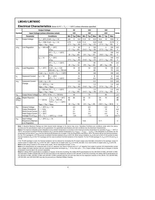
<strong>LM340</strong><strong>LM7800C</strong><br />
Electrical Characteristics (Note 4) 0C s TJ<br />
s a125C unless otherwise specified<br />
Output Voltage 5V 12V 15V<br />
Symbol Input Voltage (unless otherwise noted) 10V 19V 23V Units<br />
Parameter Conditions Min Typ Max Min Typ Max Min Typ Max<br />
V O Output Voltage T J e 25C5mAsI O s1A 48 5 52 115 12 125 144 15 156 V<br />
P D s 15W 5 mA s I O s 1A 475 525 114 126 1425 1575 V<br />
V MIN s V IN s V MAX (75 s V IN s 20) (145 s V IN s 27) (175 s V IN s 30) V<br />
DV O Line Regulation I O e 500 mA T J e 25C 3 50 4 120 4 150 mV<br />
DV IN (7 s V IN s 25) (145 s V IN s 30) (175 s V IN s 30) V<br />
0C s T J s a125C 50 120 150 mV<br />
DV IN (8 s V IN s 20) (15 s V IN s 27) (185 s V IN s 30) V<br />
I O s 1A T J e 25C 50 120 150 mV<br />
DV IN (75 s V IN s 20) (146 s V IN s 27) (177 s V IN s 30) V<br />
0C s T J s a125C 25 60 75 mV<br />
DV IN (8 s V IN s 12) (16 s V IN s 22) (20 s V IN s 26) V<br />
DV O Load Regulation T J e 25C 5mA s I O s 15A 10 50 12 120 12 150 mV<br />
250 mA s I O s 750 mA 25 60 75 mV<br />
5mAsI O s1A 0C s T J s a125C 50 120 150 mV<br />
I Q Quiescent Current I O s 1A T J e 25C 8 8 8 mA<br />
0C s T J s a125C 85 85 85 mA<br />
DI Q Quiescent Current 5 mA s I O s 1A 05 05 05 mA<br />
Change<br />
T J e 25C I O s 1A 10 10 10 mA<br />
V MIN s V IN s V MAX (75 s V IN s 20) (148 s V IN s 27) (179 s V IN s 30) V<br />
I O s 500 mA 0C s T J s a125C 10 10 10 mA<br />
V MIN s V IN s V MAX (7 s V IN s 25) (145 s V IN s 30) (175 s V IN s 30) V<br />
V N Output Noise Voltage T A e 25C 10 Hz s f s 100 kHz 40 75 90 mV<br />
DV IN<br />
DV OUT<br />
Ripple Rejection I O s 1A T J e 25C 62 80 55 72 54 70 dB<br />
f e 120 Hz or I O s 500 mA 62 55 54 dB<br />
0C s T J s a125C<br />
V MIN s V IN s V MAX (8 s V IN s 18) (15 s V IN s 25) (185 s V IN s 285) V<br />
R O Dropout Voltage T J e 25C I O e 1A 20 20 20 V<br />
Output Resistance f e 1 kHz 8 18 19 mX<br />
Short-Circuit Current T J e 25C 21 15 12 A<br />
Peak Output Current T J e 25C 24 24 24 A<br />
Average TC of V OUT 0C s T J s a125C I O e 5mA b06 b15 b18 mVC<br />
V IN Input Voltage T J e 25C I O s 1A<br />
Required to Maintain 75 146 177 V<br />
Line Regulation<br />
Note 1 Absolute Maximum Ratings are limits beyond which damage to the device may occur Operating Conditions are conditions under which the device<br />
functions but the specifications might not be guaranteed For guaranteed specifications and test conditions see the Electrical Characteristics<br />
Note 2 The maximum allowable power dissipation at any ambient temperature is a function of the maximum junction temperature for operation (TJMAX e 125C or<br />
150C) the junction-to-ambient thermal resistance (iJA) and the ambient temperature (TA) PDMAX e (TJMAX b TA)iJA If this dissipation is exceeded the die<br />
temperature will rise above TJMAX and the electrical specifications do not apply If the die temperature rises above 150C the device will go into thermal shutdown<br />
For the TO-3 package (K KC) the junction-to-ambient thermal resistance (iJA) is39CW When using a heatsink iJA is the sum of the 4CW junction-to-case<br />
thermal resistance (iJC) of the TO-3 package and the case-to-ambient thermal resistance of the heatsink For the TO-220 package (T) iJA is 54CW and iJC is<br />
4CW<br />
If the TO-263 package is used the thermal resistance can be reduced by increasing the PC board copper area thermally connected to the package Using 05<br />
square inches of copper area iJA is 50CW with 1 square inch of copper area iJA is 37GW and with 16 or more inches of copper area iJA is 32CW<br />
Note 3 ESD rating is based on the human body model 100 pF discharged through 15 kX<br />
Note 4 All characteristics are measured with a 022 mF capacitor from input to ground and a 01 mF capacitor from output to ground All characteristics except<br />
noise voltage and ripple rejection ratio are measured using pulse techniques (tw s 10 ms duty cycle s 5%) Output voltage changes due to changes in internal<br />
temperature must be taken into account separately<br />
Note 5 A military RETS specification is available on request At the time of printing the military RETS specifications for the <strong><strong>LM140</strong>A</strong>K-50883 <strong><strong>LM140</strong>A</strong>K-12883<br />
and <strong><strong>LM140</strong>A</strong>K-15883 complied with the min and max limits for the respective versions of the <strong><strong>LM140</strong>A</strong> At the time of printing the military RETS specifications for<br />
the <strong>LM140</strong>K-50883 <strong>LM140</strong>K-12883 and <strong>LM140</strong>K-15883 complied with the min and max limits for the respective versions of the <strong>LM140</strong> The <strong>LM140</strong>H883<br />
<strong>LM140</strong>K883 and <strong><strong>LM140</strong>A</strong>K883 may also be procured as a Standard Military Drawing<br />
4