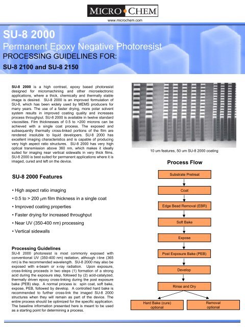
SU-8 2000 Data Sheet (2100-2150) - MicroChem
SU-8 2000 Data Sheet (2100-2150) - MicroChem
SU-8 2000 Data Sheet (2100-2150) - MicroChem

Create successful ePaper yourself
Turn your PDF publications into a flip-book with our unique Google optimized e-Paper software.
<strong>SU</strong>-8 <strong>2000</strong><br />
Permanent Epoxy Negative Photoresist<br />
PROCESSING GUIDELINES FOR:<br />
<strong>SU</strong>-8 <strong>2100</strong> and <strong>SU</strong>-8 <strong>2150</strong><br />
<strong>SU</strong>-8 <strong>2000</strong> is a high contrast, epoxy based photoresist<br />
designed for micromachining and other microelectronic<br />
applications, where a thick, chemically and thermally stable<br />
image is desired. <strong>SU</strong>-8 <strong>2000</strong> is an improved formulation of<br />
<strong>SU</strong>-8, which has been widely used by MEMS producers for<br />
many years. The use of a faster drying, more polar solvent<br />
system results in improved coating quality and increases<br />
process throughput. <strong>SU</strong>-8 <strong>2000</strong> is available in twelve standard<br />
viscosities. Film thicknesses of 0.5 to >200 microns can be<br />
achieved with a single coat process. The exposed and<br />
subsequently thermally cross-linked portions of the film are<br />
rendered insoluble to liquid developers. <strong>SU</strong>-8 <strong>2000</strong> has<br />
excellent imaging characteristics and is capable of producing<br />
very high aspect ratio structures. <strong>SU</strong>-8 <strong>2000</strong> has very high<br />
optical transmission above 360 nm, which makes it ideally<br />
suited for imaging near vertical sidewalls in very thick films.<br />
<strong>SU</strong>-8 <strong>2000</strong> is best suited for permanent applications where it is<br />
imaged, cured and left on the device.<br />
<strong>SU</strong>-8 <strong>2000</strong> Features<br />
• High aspect ratio imaging<br />
• 0.5 to > 200 μm film thickness in a single coat<br />
• Improved coating properties<br />
• Faster drying for increased throughput<br />
• Near UV (350-400 nm) processing<br />
• Vertical sidewalls<br />
Processing Guidelines<br />
<strong>SU</strong>-8 <strong>2000</strong> photoresist is most commonly exposed with<br />
conventional UV (350-400 nm) radiation, although i-line (365<br />
nm) is the recommended wavelength. <strong>SU</strong>-8 <strong>2000</strong> may also be<br />
exposed with e-beam or x-ray radiation. Upon exposure,<br />
cross-linking proceeds in two steps (1) formation of a strong<br />
acid during the exposure step, followed by (2) acid-catalyzed,<br />
thermally driven epoxy cross-linking during the post exposure<br />
bake (PEB) step. A normal process is: spin coat, soft bake,<br />
expose, PEB, followed by develop. A controlled hard bake is<br />
recommended to further cross-link the imaged <strong>SU</strong>-8 <strong>2000</strong><br />
structures when they will remain as part of the device. The<br />
entire process should be optimized for the specific application.<br />
The baseline information presented here is meant to be used<br />
as a starting point for determining a process.<br />
www.microchem.com<br />
10 um features, 50 um <strong>SU</strong>-8 <strong>2000</strong> coating<br />
Hard Bake (cure)<br />
optional<br />
Process Flow<br />
Substrate Pretreat<br />
Coat<br />
Edge Bead Removal (EBR)<br />
Soft Bake<br />
Expose<br />
Post Exposure Bake (PEB)<br />
Develop<br />
Rinse and Dry<br />
Removal<br />
optional
www.microchem.com<br />
Substrate Preparation<br />
To obtain maximum process reliability, substrates should be clean and dry<br />
prior to applying <strong>SU</strong>-8 <strong>2000</strong> resist. For best results, substrates should be<br />
cleaned with a piranha wet etch (using H 2SO 4 & H 2O 2) followed by a deionized<br />
water rinse. Substrates may also be cleaned using reactive ion<br />
etching (RIE) or any barrel asher supplied with oxygen. Adhesion<br />
promoters are typically not required. For applications that include<br />
electroplating, a pre-treatment of the substrate with MCC Primer 80/20<br />
(HMDS) is recommended.<br />
Coat<br />
<strong>SU</strong>-8 <strong>2000</strong> resists are available in twelve standard viscosities. This<br />
processing guideline document addresses two products: <strong>SU</strong>-8 <strong>2100</strong> and<br />
<strong>SU</strong>-8 <strong>2150</strong>. Figure 1. provides the information required to select the<br />
appropriate <strong>SU</strong>-8 <strong>2000</strong> resist and spin conditions to achieve the desired<br />
film thickness.<br />
Recommended Program<br />
1.) Dispense 1ml of resist for each inch (25mm) of substrate diameter.<br />
2.) Spin at 500 rpm for 5-10 seconds with acceleration of 100 rpm/second.<br />
3.) Spin at <strong>2000</strong> rpm for 30 seconds with acceleration of 300 rpm/second.<br />
Film Thickness (um)<br />
800<br />
750<br />
700<br />
650<br />
600<br />
550<br />
500<br />
450<br />
400<br />
350<br />
300<br />
250<br />
200<br />
150<br />
100<br />
50<br />
0<br />
Figure 1. <strong>SU</strong>-8 <strong>2000</strong> Spin Speed versus Thickness<br />
500 1000 1500 <strong>2000</strong> 2500 3000 3500<br />
Spin Speed (rpm)<br />
Table 1. <strong>SU</strong>-8 <strong>2000</strong> Viscosity<br />
<strong>SU</strong>-8 <strong>2150</strong><br />
<strong>SU</strong>-8 <strong>2100</strong><br />
<strong>SU</strong>-8 <strong>2000</strong> % Solids Viscosity (cSt) Density (g/ml)<br />
<strong>2100</strong> 75.00 45000 1.237<br />
<strong>2150</strong> 76.75 80000 1.238<br />
Edge Bead Removal (EBR)<br />
During the spin coat process step, a build up of photoresist may occur<br />
on the edge of the substrate. In order to minimize contamination of the<br />
hotplate, this thick bead should be removed. This can be accomplished<br />
by using a small stream of solvent (<strong>MicroChem</strong>’s EBR PG) at the edge<br />
of the wafer either at the top or from the bottom. Most automated spin<br />
coaters now have this feature and can be programmed to do this<br />
automatically.<br />
By removing any edge bead, the photomask can be placed into close<br />
contact with the wafer, resulting in improved resolution and aspect ratio.<br />
Soft Bake<br />
A level hotplate with good thermal control and uniformity is<br />
recommended for use during the Soft Bake step of the process.<br />
Convection ovens are not recommended. During convection<br />
oven baking, a skin may form on the resist. This skin can inhibit<br />
the evolution of solvent, resulting in incomplete drying of the<br />
film and/or extended bake times. Table 2. shows the<br />
recommended Soft Bake temperatures and times for the<br />
various <strong>SU</strong>-8 <strong>2000</strong> products at selected film thicknesses.<br />
Note: To optimize the baking times/conditions, remove the<br />
wafer from the hotplate after the prescribed time and allow it to<br />
cool to room temperature. Then, return the wafer to the<br />
hotplate. If the film ‘wrinkles’, leave the wafer on the hotplate for<br />
a few more minutes. Repeat the cool-down and heat-up cycle<br />
until ‘wrinkles’ are no longer seen in the film.<br />
THICKNESS SOFT BAKE TIMES<br />
(65 o C)* (95 o C)<br />
microns minutes minutes<br />
100 - 150<br />
160 - 225<br />
5<br />
5 - 7<br />
20 - 30<br />
30 - 45<br />
230 - 270 7<br />
45 - 60<br />
280 - 550 7 - 10 60 - 120<br />
Optical Parameters<br />
Table 2. Soft Bake Times<br />
The dispersion curve and Cauchy coefficients are shown in<br />
Figure 3. This information is useful for film thickness<br />
measurements based on ellipsomety and other optical<br />
measurements.<br />
<strong>SU</strong>-8 Cauchy<br />
Coefficients (uncured)<br />
n1 1.566<br />
n2 0.00796<br />
n3 0.00014<br />
Figure 3. Cauchy Coefficients
Exposure<br />
To obtain vertical sidewalls in the <strong>SU</strong>-8 <strong>2000</strong> resist, we<br />
recommend the use of a long pass filter to eliminate UV<br />
radiation below 350 nm. With the recommended filter (PL-<br />
360-LP) from Omega Optical (www.omegafilters.com) or<br />
Asahi Technoglass filters V-42 plus UV-D35<br />
(www.atgc.co.jp), an increase in exposure time of<br />
approximately 40% is required to reach the optimum<br />
exposure dose.<br />
Note: With optimal exposure, a visible latent image will be<br />
seen in the film within 5-15 seconds after being placed on the<br />
PEB hotplate and not before. An exposure matrix experiment<br />
should be performed to determine the optimum dosage.<br />
THICKNESS EXPO<strong>SU</strong>RE<br />
ENERGY<br />
microns mJ/cm 2<br />
100 - 150 240 - 260<br />
160 - 225 260 - 350<br />
230 - 270 350 - 370<br />
280 - 550 370 - 600<br />
Table 3. Exposure Dose<br />
RELATIVE DOSE<br />
Silicon 1X<br />
Glass 1.5X<br />
Pyrex 1.5X<br />
Indium Tin Oxide 1.5X<br />
Silicon Nitride 1.5 - 2X<br />
Gold 1.5 - 2X<br />
Aluminum 1.5 - 2X<br />
Nickel Iron 1.5 - 2X<br />
Copper 1.5 - 2X<br />
Nickel 1.5 - 2X<br />
Titanium 1.5 - 2X<br />
Table 4. Exposure Doses for Various Substrates<br />
Post Exposure Bake (PEB)<br />
PEB should take place directly after exposure. Table 5. shows<br />
the recommended times and temperatures<br />
Note: After 1 minute of PEB at 95°C, an image of the mask<br />
should be visible in the <strong>SU</strong>-8 <strong>2000</strong> photoresist coating. If no<br />
visible latent image is seen during or after PEB this means that<br />
there was insufficient exposure, heating or both.<br />
www.microchem.com<br />
THICKNESS PEB TIME<br />
(65 o PEB TIME<br />
C)*<br />
(95 o C)<br />
microns minutes minutes<br />
100 - 150 5<br />
10 - 12<br />
160 - 225 5<br />
12 - 15<br />
230 - 270 5<br />
15 - 20<br />
280 - 550 5<br />
20 - 30<br />
* Optional step for stress reduction<br />
Table 5. Post Exposure Bake Times<br />
Development<br />
<strong>SU</strong>-8 <strong>2000</strong> photoresist has been designed for use in immersion,<br />
spray or spray-puddle processes with <strong>MicroChem</strong>’s <strong>SU</strong>-8<br />
developer. Other solvent based developers such as ethyl lactate<br />
and diacetone alcohol may also be used. Strong agitation is<br />
recommended when developing high aspect ratio and/or thick<br />
film structures. The recommended development times for<br />
immersion processes are given in Table 6. These development<br />
times are approximate, since actual dissolution rates can vary<br />
widely as a function of agitation<br />
Note: The use of an ultrasonic or megasonic bath may be<br />
helpful when developing out via or hole patterns or structures<br />
with tight pitch.<br />
THICKNESS DEVELOPMENT<br />
TIME<br />
microns minutes<br />
100 - 150 10 - 15<br />
160 - 225 15 - 17<br />
230 - 270 17 - 20<br />
280 - 550 20 - 30<br />
Table 6. Development Times for <strong>SU</strong>-8 Developer<br />
Rinse and Dry<br />
When using <strong>SU</strong>-8 developer, spray and wash the developed<br />
image with fresh solution for approximately 10 seconds,<br />
followed by a second spray/wash with Isopropyl Alcohol (IPA)<br />
for another 10 seconds. Air dry with filtered, pressurized air or<br />
nitrogen.<br />
Note: A white film produced during IPA rinse is an indication<br />
of underdevelopment of the unexposed photoresist. Simply<br />
immerse or spray the substrate with additional <strong>SU</strong>-8 developer<br />
to remove the white film and complete the development<br />
process. Repeat the rinse step.<br />
The use of an ultrasonic or megasonic bath will energize the<br />
solvent and allow for more effective development of the<br />
unexposed resist.
Transmittance (%)<br />
Physical Properties<br />
(Approximate values)<br />
Adhesion Strength (mPa) Silicon/Glass/Glass & HMDS 38/35/35<br />
Glass Transition Temperature (Tg °C), tan δ peak 210<br />
Thermal Stability (°C @ 5% wt. loss) 315<br />
Thermal Conductivity (W/mK) 0.3<br />
Coeff. of Thermal Expansion (CTE ppm) 52<br />
Tensile Strength (Mpa) 60<br />
Elongation at break (εb %) 6.5<br />
Young’s Modulus (Gpa) 2.0<br />
Dielectric Constant @ 10MHz 3.2<br />
Water Absorption (% 85<br />
o C/85 RH)<br />
Optical Properties<br />
100<br />
90<br />
80<br />
70<br />
60<br />
50<br />
40<br />
30<br />
20<br />
10<br />
Table 7. Physical Propeties<br />
Figure 4. Optical Transmittance<br />
0<br />
320 360 400 440 480 520 560 600 640 680 720 760 800<br />
Wavelength (nm)<br />
Process conditions for Figure 4.<br />
Softbake: 5 minutes at 95°C<br />
Exposure: 180 mJ/cm 2<br />
Hardbake: 30 minutes at 300°C<br />
After Softbake<br />
After Exposure<br />
After Hardbake<br />
0.65<br />
Hard Bake (cure)<br />
<strong>SU</strong>-8 <strong>2000</strong> has good mechanical properties. However, for<br />
applications where the imaged resist is to be left as part of the<br />
final device, a hard bake can be incorporated into the process.<br />
This is generally only required if the final device or part is to be<br />
subject to thermal processing during regular operation. A hard<br />
bake or final cure step is added to ensure that <strong>SU</strong>-8 <strong>2000</strong><br />
properties do not change in actual use. <strong>SU</strong>-8 <strong>2000</strong> is a thermal<br />
resin and as such its properties can continue to change when<br />
exposed to a higher temperature than previously encountered.<br />
We recommend using a final bake temperature 10°C higher than<br />
the maximum expected device operating temperature.<br />
Depending on the degree of cure required, a bake temperature in<br />
the range of 150°C to 250°C and for a time between 5 and 30<br />
minutes is typically used.<br />
www.microchem.com<br />
Note: The hard bake step is also useful for annealing any<br />
surface cracks that may be evident after development. The<br />
recommended step is to bake at 150°C for a couple of<br />
minutes. This applies to all film thicknesses.<br />
Removal<br />
<strong>SU</strong>-8 <strong>2000</strong> has been designed as a permanent, highly crosslinked<br />
epoxy material and it is extremely difficult to remove it<br />
with conventional solvent based resist strippers. <strong>MicroChem</strong>’s<br />
Remover PG will swell and lift off minimally cross-linked <strong>SU</strong>-8<br />
<strong>2000</strong>. However, if OmniCoat (30-100 nm) has been applied,<br />
immersion in Remover PG can effect a clean and thorough<br />
Lift-Off of the <strong>SU</strong>-8 <strong>2000</strong> material. Fully cured or hard baked<br />
<strong>SU</strong>-8 <strong>2000</strong> cannot be removed without the use of OmniCoat.<br />
To remove minimally cross-linked <strong>SU</strong>-8 <strong>2000</strong>, or when using<br />
Omnicoat: Heat the Remover PG bath to 50-80°C and<br />
immerse the substrates for 30-90 minutes. Actual strip time will<br />
depend on resist thickness and cross-link density For more<br />
information on <strong>MicroChem</strong> Omnicoat and Remover PG please<br />
see the relevant product data sheets.<br />
To re-work fully cross-linked <strong>SU</strong>-8 <strong>2000</strong>: Wafers can be<br />
stripped using oxidizing acid solutions such as piranha etch,<br />
plasma ash, RIE, laser ablation and pyrolysis.<br />
Plasma Removal<br />
RIE 200W, 80 sccm O2, 8 sccm CF4, 100mTorr, 10°C<br />
Storage<br />
Store <strong>SU</strong>-8 <strong>2000</strong> resists upright and in tightly closed<br />
containers in a cool, dry environment away from direct sunlight<br />
at a temperature of 40-70°F (4-21°C). Store away from light,<br />
acids, heat and sources of ignition. Shelf life is thirteen months<br />
from date of manufacture.<br />
Disposal<br />
<strong>SU</strong>-8 <strong>2000</strong> resists may be included with other waste<br />
containing similar organic solvents to be discarded for<br />
destruction or reclaim in accordance with local state and<br />
federal regulations. It is the responsibility of the customer to<br />
ensure the disposal of <strong>SU</strong>-8 <strong>2000</strong> resists and residues made<br />
in observance all federal, state, and local environmental<br />
regulations.
Environmental, Health and Safety<br />
Consult the product Material Safety <strong>Data</strong> <strong>Sheet</strong> before working<br />
with <strong>SU</strong>-8 <strong>2000</strong> resists. Handle with care. Wear chemical<br />
goggles, chemical gloves and suitable protective clothing when<br />
handling <strong>SU</strong>-8 <strong>2000</strong> resists. Do not get into eyes, or onto skin or<br />
clothing. Use with adequate ventilation to avoid breathing vapors<br />
or mist. In case of contact with skin, wash affected area with<br />
soap and water. In case of contact with eyes, rinse immediately<br />
with water and flush for 15 minutes lifting eyelids frequently. Get<br />
emergency medical assistance.<br />
The information is based on our experience and is, we believe to<br />
be reliable, but may not be complete. We make no guarantee or<br />
warranty, expressed or implied, regarding the information, use,<br />
handling, storage, or possession of these products, or the<br />
application of any process described herein or the results<br />
desired, since the conditions of use and handling of these<br />
products are beyond our control.<br />
Disclaimer<br />
Notwithstanding anything to the contrary contained in any sales<br />
documentation, e.g., purchase order forms, all sales are made<br />
on the following conditions:<br />
All information contained in any <strong>MicroChem</strong> product literature<br />
reflects <strong>MicroChem</strong>’s current knowledge on the subject and is,<br />
we believe, reliable. It is offered solely to provide possible<br />
suggestions for customer’s own experiments and is not a<br />
substitute for any testing by customer to determine the suitability<br />
of any of <strong>MicroChem</strong> products for any particular purpose. This<br />
information may be subject to revision as new knowledge and<br />
experience becomes available, but <strong>MicroChem</strong> assumes no<br />
obligation to update or revise any data previously furnished to a<br />
customer; and if currency of data becomes an issue, customer<br />
should contact <strong>MicroChem</strong> requesting updates. Since<br />
<strong>MicroChem</strong> cannot anticipate all variations in actual end uses or<br />
in actual end-use conditions, it makes no claims, representations<br />
or warranties, express or implied including, without limitation any<br />
warranty of merchantability or fitness for a particular purpose;<br />
and customer waives all of the same. <strong>MicroChem</strong> expressly<br />
disclaims any responsibility or liability and assumes no<br />
responsibility or liability in connection with any use of this<br />
information including, without limitation, any use, handling,<br />
storage or possession of any <strong>MicroChem</strong> products, or the<br />
application of any process described herein or the results<br />
desired or anything relating to the design of the customer’s<br />
products. Nothing in this publication is to be considered as a<br />
license to operate under or a recommendation to infringe any<br />
patent right.<br />
www.microchem.com<br />
Caution<br />
This product is not designed or manufactured for, nor is it<br />
intended for use in any medical device or for any other medical<br />
application. Do not use this product in any medical<br />
applications [including, without limitation, any permanent<br />
implantation in the human body or any animals (other than<br />
laboratory animals used for experimental purposes), or contact<br />
with internal body fluids or tissues] unless otherwise expressly<br />
and specifically provided for in a written contract between MCC<br />
and the customer. The complete <strong>MicroChem</strong> Medical<br />
Disclaimer Statement is available upon request or on the<br />
<strong>MicroChem</strong> website at www.microchem.com.<br />
1254 Chestnut St.<br />
Newton, MA 02464<br />
PHONE: 617.965.5511<br />
FAX: 617.965.5818<br />
EMAIL: sales@ microchem.com<br />
www.microchem.com