analysis of terahertz wave propagation in gap plasmon waveguide ...
analysis of terahertz wave propagation in gap plasmon waveguide ...
analysis of terahertz wave propagation in gap plasmon waveguide ...

You also want an ePaper? Increase the reach of your titles
YUMPU automatically turns print PDFs into web optimized ePapers that Google loves.
Armenian Journal <strong>of</strong> Physics, 2010, vol. 3, issue 1, pp. 69–77<br />
ANALYSIS OF TERAHERTZ WAVE PROPAGATION<br />
IN GAP PLASMON WAVEGUIDE<br />
FORMED BY TWO CYLINDERS<br />
Yu. H. Avetisyan, H. Hakopyan, A. H. Makaryan, and Kh.V.Nerkararyan<br />
Department <strong>of</strong> Radiophysics, Yerevan State University, Yerevan, 1 Alek Manoogian, Armenia<br />
yuriav@ysu.am<br />
Received February 10, 2010<br />
Abstract - The simple theoretical model is developed to calculate effective <strong>in</strong>dex and field distribution <strong>of</strong> the<br />
fundamental TM0-mode <strong>in</strong> <strong>gap</strong> <strong>plasmon</strong> <strong>wave</strong>guide formed by two cyl<strong>in</strong>drical surfaces made <strong>of</strong> gold, doped Si, and<br />
polyv<strong>in</strong>ylidene fluoride (PVDF) materials. It is shown that doped Si and PVDF are promis<strong>in</strong>g materials for strongly<br />
conf<strong>in</strong>ed THz-<strong>wave</strong> <strong>propagation</strong> <strong>in</strong> <strong>gap</strong> <strong>plasmon</strong> <strong>wave</strong>guide. Though mode conf<strong>in</strong>ement <strong>in</strong> metal <strong>wave</strong>guide is lower, it<br />
is preferable for low-loss undistorted <strong>propagation</strong> <strong>of</strong> the broadband THz-pulses.<br />
Key Words: <strong>terahertz</strong>, <strong>plasmon</strong> <strong>wave</strong>guides, THz time-doma<strong>in</strong> spectroscopy<br />
1. Introduction<br />
Recently, <strong>plasmon</strong> <strong>wave</strong>guides have attracted much attention due to its potential to guide light<br />
<strong>in</strong> a region beyond the so-called diffraction limit [1-3]. At optical frequencies, many metals support<br />
fasc<strong>in</strong>at<strong>in</strong>g optical <strong>in</strong>teractions such as surface <strong>plasmon</strong>s polaritons (SPPs) because the dielectric<br />
constant <strong>of</strong> metals <strong>in</strong> the visible and near-IR regions is predom<strong>in</strong>antly real and negative. It would be<br />
greatly advantageous to take concepts <strong>of</strong> SPP to obta<strong>in</strong> sub<strong>wave</strong>length conf<strong>in</strong>ed guided-<strong>wave</strong><br />
<strong>propagation</strong> at <strong>terahertz</strong> (THz) frequencies. For its unique characters, THz-<strong>wave</strong>s have many<br />
applications <strong>in</strong> scientific research and application fields, such as spectroscopy, free space<br />
communication, environmental sens<strong>in</strong>g and medical imag<strong>in</strong>g [4]. Dur<strong>in</strong>g last decade, THz<br />
technology has made great progress due to the rapid development <strong>of</strong> radiation sources [5–7] and<br />
detectors [8, 9], while strongly 2-dimentional (D) conf<strong>in</strong>ed <strong>propagation</strong> <strong>in</strong> <strong>wave</strong>guides is also vitally<br />
important to the development <strong>of</strong> THz technology. Though most studies <strong>of</strong> SPPs focus on the visible<br />
and <strong>in</strong>frared regions, the SPPs <strong>propagation</strong> on metal flat surfaces [10, 11] and wires [12, 13] for<br />
THz regime is <strong>in</strong>vestigated as well.<br />
The ma<strong>in</strong> problem <strong>of</strong> THz-SPPs excitation <strong>in</strong> metals is large value <strong>of</strong> plasma frequency,<br />
2 2 2<br />
which is def<strong>in</strong>ed by Ne 4 m , where N is the electron density, e electron charge, ε0 is the<br />
p e<br />
0<br />
vacuum permittivity and me electron mass. S<strong>in</strong>ce the free electron density <strong>in</strong> metals is typically <strong>of</strong><br />
the order <strong>of</strong> 10 22 cm 3 , the plasma frequency is limited to the visible and ultraviolet regions. At<br />
frequencies significantly below the plasma frequency (like the THz range), large negative<br />
permittivity strongly prohibits electromagnetic fields from penetration <strong>in</strong>side a metal, and <strong>plasmon</strong><br />
excitation on the metal-dielectric <strong>in</strong>terface becomes challeng<strong>in</strong>g.
70<br />
Armenian Journal <strong>of</strong> Physics, 2010, vol. 3, issue 1<br />
There are different approaches which makes possible to decrease plasma frequency. Recently<br />
it was demonstrated that a periodic lattice <strong>of</strong> th<strong>in</strong> metallic wires could exhibit a plasma frequency<br />
even <strong>in</strong> micro<strong>wave</strong> [14]. However, many periods <strong>of</strong> such a structure are required that is a limit<strong>in</strong>g<br />
factor to the use <strong>of</strong> such media <strong>in</strong> practical applications. Besides, the periodic lattice <strong>of</strong> th<strong>in</strong> metallic<br />
wires is difficult and expensive to produce. An alternative composite media are structured metal<br />
surfaces with periodical groves or holes. This medium is characterized by an effective permittivity<br />
that has a <strong>plasmon</strong> form with a plasma frequency dictated by the geometry <strong>of</strong> the hole or the groove<br />
[15]. However, effective permittivity <strong>of</strong> the periodical structures is strongly frequency dependent<br />
that limit operation bandwidth <strong>of</strong> <strong>plasmon</strong>ic devices.<br />
In this paper we are focus<strong>in</strong>g on media hav<strong>in</strong>g plasma frequency well below that <strong>of</strong> metals,<br />
which do not depend on the use <strong>of</strong> components with dimensions related to the frequency <strong>of</strong> <strong>in</strong>terest.<br />
The doped semiconductors are good alternatives to metals for the excitation <strong>of</strong> low-frequency<br />
<strong>plasmon</strong>s [16]. As the carrier densities <strong>in</strong> semiconductors are much lower than those <strong>in</strong> metals, the<br />
plasma frequency is much smaller, be<strong>in</strong>g typically at mid- or far-<strong>in</strong>frared frequencies. Therefore,<br />
the permittivity <strong>of</strong> semiconductors at THz is comparable to that <strong>of</strong> metals at optical frequencies. A<br />
decisive advantage <strong>of</strong> semiconductors is that their carrier density and mobility, and consequently<br />
the SPPs, can be easily controlled by thermal or optical excitation <strong>of</strong> free carriers. However, the<br />
doped semiconductors usually have large imag<strong>in</strong>ary part <strong>of</strong> the complex permittivity that limits SPP<br />
<strong>propagation</strong> length.<br />
It has been known for some time that low-frequency <strong>plasmon</strong>s can be observed <strong>in</strong> <strong>in</strong>tr<strong>in</strong>sically<br />
conduct<strong>in</strong>g polymers [17]. Quite recently porous fiber with ferroelectric polyv<strong>in</strong>ylidene fluoride<br />
(PVDF) polymer was proposed as a surface <strong>plasmon</strong> resonance (SPR) sensor [18]. The PVDF film<br />
(usually used <strong>in</strong> piezoelectric devices) is widely commercially available and it can be easily bonded<br />
to different substrates <strong>in</strong>clud<strong>in</strong>g metals. Moreover, a use <strong>of</strong> PVDF gives an opportunity to design a<br />
fully polymeric THz <strong>plasmon</strong>ic structure, which potentially makes the fabrication process highly<br />
suitable for the <strong>in</strong>dustrial scale-up.<br />
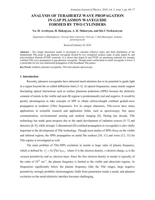
In this paper we present the characteristics <strong>of</strong> THz-<strong>wave</strong> <strong>propagation</strong> <strong>in</strong> <strong>gap</strong> Plasmon<br />
Waveguide formed by two Cyl<strong>in</strong>drical Surfaces (PWCS), made <strong>of</strong> metal, semiconductor, and PVDF<br />
(Fig. 1).<br />
R<br />
L<br />
y<br />
h(y)<br />
x<br />
Fig. 1. Schematic view <strong>of</strong> the <strong>wave</strong>guide
71<br />
Armenian Journal <strong>of</strong> Physics, 2010, vol. 3, issue 1<br />
The analytic description CPP modes <strong>in</strong> <strong>gap</strong> PWCS with metal surfaces has been recently<br />
obta<strong>in</strong>ed <strong>in</strong> optical regime [19]. Here the simple way to calculate fundamental TM0 mode sizes and<br />
dispersion <strong>in</strong> THz region is presented. Waveguide is considered as parallel plate <strong>wave</strong>guide<br />
(PPWG) with adiabatically vary<strong>in</strong>g distance between plates h(y). It is known [20] that effective<br />
refractive <strong>in</strong>dex at TM0 mode <strong>in</strong> <strong>plasmon</strong> PPWG is approximately <strong>in</strong>versely proportional to the<br />
distance between plates, Neff ~ 1/h(y). Therefore the model <strong>of</strong> graded-<strong>in</strong>dex dielectric <strong>wave</strong>guide<br />
[21] can be used to calculate THz-<strong>wave</strong> conf<strong>in</strong>ement along the y-axis.<br />
2. Complex permittivity <strong>of</strong> materials <strong>in</strong> the THz range<br />
In order to model the <strong>gap</strong> PWCS, the complex permittivity <strong>of</strong> cyl<strong>in</strong>drical surfaces (made <strong>of</strong> metal or<br />
doped semiconductors) was assumed to be Drude-like, which corresponds to the approximation <strong>of</strong> a<br />
s<strong>in</strong>gle energy <strong>in</strong>dependent scatter<strong>in</strong>g time, [22]. This quantity can be related to the dc mobility, ,<br />
takes the<br />
by = e /m*. Then the frequency-dependent complex permittivity ' i"<br />
form<br />
2<br />
p<br />
,<br />
(1)<br />
<br />
i <br />
where p is the plasma frequency, is the damp<strong>in</strong>g rate (<strong>in</strong>verse scatter<strong>in</strong>g time) <strong>of</strong> the carriers, and<br />
ε is the permittivity at extremely high frequencies that is unity for metals or permittivity <strong>of</strong><br />
undoped material for semiconductors.<br />
When <strong>wave</strong>guide’s cyl<strong>in</strong>ders are made <strong>of</strong> PVDF, the material dispersion is given by<br />
<br />
2<br />
dc opt 0<br />
opt ,<br />
(2)<br />
i<br />
2 2<br />
0<br />
where εopt is the optical dielectric constant, εdc is the low-frequency (dc) dielectric constant, 0 is<br />
the frequency <strong>of</strong> the transverse-optical mode <strong>of</strong> the material.<br />
Us<strong>in</strong>g Eq.(1) with p and given <strong>in</strong> Ref. [23], the complex permittivities <strong>of</strong> the different<br />
high-conductivity metals have been calculated <strong>in</strong> 0.1–3 THz region. In all cases the negative real<br />
part <strong>of</strong> has an order <strong>of</strong> 10 5 . Because THz region is far enough from plasma frequency p the<br />
value <strong>of</strong> ' is practically <strong>in</strong>dependent <strong>of</strong> frequency. For <strong>in</strong>stance, <strong>in</strong> gold<br />
and it is slowly reduced to<br />
5<br />
' 1.14 10 at 0.1 THz<br />
5<br />
' 0.94 10 at 3 THz. Such small dispersion is very attractive for<br />
<strong>plasmon</strong>ic <strong>wave</strong>guides operat<strong>in</strong>g <strong>in</strong> a wide frequency region. The imag<strong>in</strong>ary part <strong>of</strong> the permittivity<br />
<strong>in</strong> metals (which is related to dissipation) is usually 3–10 times larger than ', whereas <strong>in</strong> the<br />
optical region ' ".<br />
For gold the ratio ' " is 0.16 for 1THz, whereas it is ' " 13 for<br />
300 THz (λ = 1 m).
72<br />
Armenian Journal <strong>of</strong> Physics, 2010, vol. 3, issue 1<br />
The doped silicon is chosen to illustrate the behavior <strong>of</strong> permittivity <strong>of</strong> the doped<br />
semiconductors. The silicon’s characteristics <strong>in</strong> THz range are well established [22] and it is widely<br />
available and cheapest semiconductor material. In addition, silicon already used <strong>in</strong> many studies<br />
related to SPP-assisted THz-<strong>wave</strong> transmission through array <strong>of</strong> holes [24, 25]. For n-doped Si<br />
(with N = 10 18 cm 3 and N = 10 17 cm 3 ) the dependences <strong>of</strong> real and imag<strong>in</strong>ary parts <strong>of</strong> the<br />
permittivity on the frequency were calculated with Eq.(1). Because the scatter<strong>in</strong>g time <strong>of</strong> carriers<br />
depends on their density, the values <strong>of</strong> have been assumed = 1.35 THz for N = 10 17 cm 3 and<br />
= 4.1 THz for N = 10 18 cm -3 <strong>in</strong> accordance to Baccarani–Ostaja model [26]. The calculated<br />
dependencies <strong>of</strong> '<br />
and " <br />
<strong>in</strong> Fig.2.<br />
for doped Si with N = 10 18 cm -3 and N = 10 17 cm 3 are presented<br />
As it is seen <strong>in</strong> Fig. 2, the lightly doped silicon (N = 10 17 cm -3 ) has negative ε only for<br />
< 0.9 THz and therefore it cannot support SPP-mode excitation at the <strong>in</strong>terface air–Si for higher<br />
frequencies. The dop<strong>in</strong>g with free carrier concentration N = 10 18 cm 3 is quite sufficient to have<br />
negative real part <strong>of</strong> as far as 3 THz. The last value is close to highest frequency <strong>of</strong> the common<br />
time-doma<strong>in</strong> spectroscopy (TDS) systems.<br />
The calculated dependences <strong>of</strong> the real and imag<strong>in</strong>ary parts <strong>of</strong> PVDF permittivity on the<br />
frequency are presented <strong>in</strong> Fig. 3. The follow<strong>in</strong>g values <strong>of</strong> 0 = 0.3 THz, εopt = 2, εdc = 50, and<br />
= 0.1 THz have been used <strong>in</strong> Eq.(2), accord<strong>in</strong>gly to [27].<br />
Fig. 3 shows that <strong>plasmon</strong>-like SPP excitation may be carried out <strong>in</strong> the frequency range<br />
from 0.4 THz to 1.4 THz. The upper limit is determ<strong>in</strong>ed by the condition ε' < 0 and lower limit is<br />
related to necessity <strong>of</strong> the relatively small value <strong>of</strong> ε'', i.e. low absorption. Thus the use <strong>of</strong> PVDF <strong>in</strong><br />
<strong>plasmon</strong> THz devices is limited by narrowband applications <strong>in</strong> the range <strong>of</strong> approximately 0.41.4<br />
THz.<br />
ε'<br />
5<br />
0<br />
5<br />
N=10 18 cm -3<br />
10 17<br />
10 18<br />
10 17<br />
0.5 1 1.5<br />
Frequency, THz<br />
2 2.5<br />
Fig. 2. Dependences <strong>of</strong> the negative real and imag<strong>in</strong>ary parts <strong>of</strong> doped Si on the frequency for carrier<br />
concentrations N=10 17 cm -3 and N=10 18 cm -3<br />
ε''<br />
200<br />
100
73<br />
Armenian Journal <strong>of</strong> Physics, 2010, vol. 3, issue 1<br />
Fig. 3. Dependences <strong>of</strong> the negative real and imag<strong>in</strong>ary parts <strong>of</strong> PVDF on the frequency.<br />
3. Effective <strong>in</strong>dex <strong>of</strong> PPWG<br />
In this section, we calculate the effective refractive <strong>in</strong>dex <br />
(vph is the phase velocity,<br />
Re n c v ph<br />
c is the velocity <strong>of</strong> light) <strong>of</strong> PPWG formed by two <strong>in</strong>f<strong>in</strong>ite parallel plates <strong>in</strong> the YZ plane (see Fig.<br />
1). The plate’s separation h0 is chosen equal to the m<strong>in</strong>imal distance between cyl<strong>in</strong>drical surfaces<br />
h(y=0) <strong>of</strong> the PWCS. Here obta<strong>in</strong>ed results will be used <strong>in</strong> the next section to calculate <strong>propagation</strong><br />
characteristics <strong>of</strong> real PWCS.<br />
The dispersion <strong>of</strong> SPP-mode <strong>in</strong> PPWG filled with air is given by the expression [2]<br />
k h n<br />
<br />
2 n<br />
1<br />
2 2<br />
0 0 2 <br />
tanh n<br />
1 0,<br />
2<br />
where k0 = 2π /c is the <strong>wave</strong>number <strong>in</strong> air, is the complex permittivity <strong>of</strong> the plates material.<br />
Us<strong>in</strong>g the calculated (<strong>in</strong> section 2) complex permittivities for doped Si, PVDF, and Au,<br />
the numerical solution <strong>of</strong> (3) is obta<strong>in</strong>ed. The dependences <strong>of</strong> n coefficient k n 0 Im<br />
ε'<br />
40<br />
30<br />
20<br />
10<br />
10<br />
(3)<br />
Re 1<br />
and absorption<br />
on the frequency for PPWG with h0 = 0.1 mm, and plates made <strong>of</strong> doped<br />
Si (N = 10 18 cm -3 ) and gold <strong>in</strong> the range 0.13 THz are presented <strong>in</strong> Fig. 4. For convenience <strong>of</strong> the<br />
presentation the values correspond<strong>in</strong>g to gold covered PPWG are <strong>in</strong>creased 50 times.<br />
While the absorption coefficient <strong>in</strong> gold-PPWG is small ( = 7.610 -3 mm 1 ), the effective<br />
refractive <strong>in</strong>dex is too close to 1. As we shall be conv<strong>in</strong>ced below, the relatively large value <strong>of</strong> is<br />
favorable to have the strong field conf<strong>in</strong>ement <strong>in</strong> lateral direction (along the y-axis) <strong>of</strong> <strong>gap</strong> PWCS.<br />
In PPWG with plates made <strong>of</strong> doped Si the effective refractive <strong>in</strong>dex n more appreciably differs<br />
from 1. Though absorption losses are significantly stronger, use <strong>of</strong> the doped Si can be suitable for<br />
chip-scale THz <strong>wave</strong> guid<strong>in</strong>g.<br />
0<br />
0.8 1.2 1.6<br />
Frequency, THz<br />
ε''<br />
10 1<br />
10 0<br />
10 -1
74<br />
Armenian Journal <strong>of</strong> Physics, 2010, vol. 3, issue 1<br />
Fig. 4. The dependences <strong>of</strong> and absorption coefficient on the frequency for PPWG made <strong>of</strong> doped Si with<br />
N = 10 18 cm -3 (red and green l<strong>in</strong>es) and gold (blue and violet). In the last case calculated values <strong>of</strong> and are<br />
<strong>in</strong>creased 50 times.<br />
Figure 5 illustrates the dependences <strong>of</strong> and on the frequency for PVDF covered PPWG.<br />
Fig. 5. The dependences <strong>of</strong> (red l<strong>in</strong>e) and absorption coefficient (blue l<strong>in</strong>e) on the frequency for PPWG made<br />
<strong>of</strong> PVDF.<br />
It is seen that attenuation <strong>of</strong> THz-<strong>wave</strong> is strongly enhanced with growth <strong>of</strong> the frequency<br />
s<strong>in</strong>ce nearly 1 THz. Hence it is expedient to limit the operation bandwidth <strong>of</strong> the PVDF-based<br />
<strong>wave</strong>guides by frequencies 0.41 THz. The ma<strong>in</strong> advantage <strong>of</strong> PVDF us<strong>in</strong>g is relatively large value<br />
<strong>of</strong> that is favorable to obta<strong>in</strong> small mode size <strong>in</strong> lateral direction <strong>of</strong> PWCS.<br />
4. Effective <strong>in</strong>dex <strong>of</strong> PWCS<br />
<br />
0.06<br />
0.04<br />
0.02<br />
<br />
0.4<br />
0.2<br />
0<br />
0 1 2<br />
Frequency, THz<br />
0.6 0.8<br />
Frequency, THz<br />
1<br />
The effective refractive <strong>in</strong>dex Neff = c/Vph (where Vph is the phase velocity <strong>in</strong> PWCS) <strong>of</strong><br />
PWCS is calculated by consider<strong>in</strong>g it as PPWG with adiabatically vary<strong>in</strong>g plate’s separation. Us<strong>in</strong>g<br />
notations shown <strong>in</strong> Fig. 1, the distance between cyl<strong>in</strong>drical surfaces <strong>of</strong> PWCS can be written as<br />
2<br />
1<br />
mm <br />
mm -1<br />
3<br />
2<br />
1
where R is the radius <strong>of</strong> cyl<strong>in</strong>ders and condition y
76<br />
Armenian Journal <strong>of</strong> Physics, 2010, vol. 3, issue 1<br />
reason it is not shown <strong>in</strong> Fig. 6a. It is seen that field distributions are frequency dependent as it was<br />
generally expected. In case <strong>of</strong> Si-based PWCS the electrical field is more strongly concentrated <strong>in</strong><br />
the vic<strong>in</strong>ity <strong>of</strong> middle <strong>of</strong> the <strong>wave</strong>guide (y = 0) than that <strong>of</strong> Au-based PWCS. It is related to<br />
relatively small for Si material.<br />
Intensity, a.u.<br />
1<br />
0.5<br />
(a)<br />
Fig. 6. The fundamental mode <strong>in</strong>tensities distributions <strong>in</strong> PWCS made <strong>of</strong> doped Si (a) and Au (b) at the<br />
frequencies 1 THz (red l<strong>in</strong>e) and 0.4 THz (blue dotted l<strong>in</strong>e).<br />
The dispersion <strong>of</strong> the effective <strong>in</strong>dex <strong>of</strong> <strong>wave</strong>guide Neff is very important for applications <strong>of</strong><br />
PWCS with broadband THz radiation, such as THz-pulse. The calculated dependences<br />
Neff = Neff() are nearly same that <strong>of</strong> n = n() for correspond<strong>in</strong>g PPWG (see Fig. 4). For Au-based<br />
PWCS the value <strong>of</strong> Neff is very close to 1 <strong>in</strong>dependently <strong>of</strong> frequency. For Si-based PWCS the value<br />
<strong>of</strong> Neff is 1.076 at 0.1 THz and it is reduced to 1.026 at 3 THz. Even such small dispersion <strong>of</strong> the<br />
<strong>wave</strong>guide limits its application with broadband THz-pulses. Indeed, after propagat<strong>in</strong>g 3 mm<br />
distance the delay <strong>of</strong> spectral components at 0.1 THz and 3 THz is 0.5 ps, which is close to duration<br />
<strong>of</strong> the THz-pulses commonly used <strong>in</strong> practice.<br />
5. Conclusions<br />
-2 0<br />
y, mm<br />
2 4<br />
A simple theoretical model is developed to calculate effective <strong>in</strong>dex and field distribution <strong>of</strong><br />
the fundamental TM0-mode <strong>in</strong> <strong>gap</strong> <strong>plasmon</strong> <strong>wave</strong>guide formed by two cyl<strong>in</strong>drical surfaces made <strong>of</strong><br />
gold, doped Si, and polyv<strong>in</strong>ylidene fluoride (PVDF) materials. It is shown that doped Si and PVDF<br />
are good candidates for <strong>plasmon</strong> <strong>wave</strong>guides support<strong>in</strong>g strongly conf<strong>in</strong>ed THz-<strong>wave</strong> <strong>propagation</strong>.<br />
While mode conf<strong>in</strong>ement <strong>in</strong> metal <strong>wave</strong>guide is lower, it is preferable for low-loss undistorted<br />
<strong>propagation</strong> <strong>of</strong> the broadband THz-pulses.<br />
Intensity, a.u.<br />
References<br />
1. K. Tanaka and M. Tanaka, Appl. Phys. Lett. v. 82, 1158 (2003).<br />
2. Plasmonic Nanoguides and Circuits, ed. by S. Bozhevolnyi, Pan Stanford, S<strong>in</strong><strong>gap</strong>ore, 2008.<br />
1<br />
0.5<br />
(b)<br />
-7.5 0<br />
y, mm<br />
7.5 15
77<br />
Armenian Journal <strong>of</strong> Physics, 2010, vol. 3, issue 1<br />
3. Y. Matsuzaki, T. Okamoto, M. Haraguchi, M. Fukui, and M. Nakagaki, Opt. Exp. 16,<br />
16314 (2008).<br />
4. M.Tonouchi, Nat. Photon. 1, 97 (2007).<br />
5. T. D. Wang, S. T. L<strong>in</strong>, Y. Y. L<strong>in</strong>, A. C. Chiang, and Y. C. Huang, Opt. Express, 16, 6471<br />
(2008).<br />
6. K. L. Vodopyanov and Yu. H. Avetisyan, Opt. Lett. 33, 2314 (2008).<br />
7. P. E. Powers, R. A. Alkuwari, J. W. Haus, K. Suizu, and H. Ito, Opt. Lett. 30, 640 (2005).<br />
8. K. Sakai, Terahertz Optoelectronics, Spr<strong>in</strong>ger, Berl<strong>in</strong>, 2005.<br />
9. A. Leitenstorfer, S. Hunsche, J. Shah, M. C. Nuss, and W. H. Knox, Appl. Phys. Lett. 74,<br />
1516 (1999).<br />
10. T.-I. Jeon and D. Grischkowsky, Appl. Phys. Lett. 88, 061113 (2006).<br />
11. J. F. O’Hara, R. D. Averitt, and A. J. Taylor, Opt. Express 12, 6397 (2004).<br />
12. K. Wang and D. M. Mittleman, Phys. Rev. Lett. 96, 157401 (2006).<br />
13. M. Wächter, M. Nagel, and H. Kurz, Opt. Express 13, 10815 (2005).<br />
14. J. B. Pendry , A. J. Holden, W. J. Stewart, and I. Youngs, Phys. Rev. Lett., 76, 4773 (1996).<br />
15. J. B. Pendry, L. M. Moreno, and F. J. Garcia-Vidal, Science 305, 847 (2004).<br />
16. J. G. Rivas, M. Kuttge, H. Kurz, P. H. Bolivar, and J. A. Sánchez-Gil, Appl. Phys. Lett. 88,<br />
082106 (2006).<br />
17. R. Kohlman et al., Handbook <strong>of</strong> Conduct<strong>in</strong>g Polymers, Ed. Skotheim, Elsenbaumer and<br />
Reynolds, Marcel Dekker, New York 1998.<br />
18. A. Hassani, and M. Skorobogatiy, <strong>in</strong> CLEO/QELS-2009 (Optical Society <strong>of</strong> America,<br />
Wash<strong>in</strong>gton, DC, 2009), CM16.<br />
19. S. I. Bozhevolnyi and Kh. V. Nerkararyan, Opt. Express 17, 10327 (2009).<br />
20. B. Ghamsari and H. Majedi, J. Appl. Phys. 104, 083108 (2008).<br />
21. H. Kogelnik, Guided-Wave Optoelectronics, 2nd ed. Spr<strong>in</strong>ger-Verlag, Berl<strong>in</strong>, 1990.<br />
22. T.-I. Jeon and D. Grischkowsky, Phys. Rev. Lett. 78, 1106 (1997).<br />
23. M. A. Ordal, R. J. Bell, R. W. Alexander, Jr. L. Long, and M. R. Querry, Appl. Opt., 24,<br />
4493 (1985).<br />
24. J. G. Rivas, C. Schotsch, P. H. Bolivar, and H. Kurz, Phys. Rev. B 68, 201306 (2003).<br />
25. E. Hendry, F. J. Garcia-Vidal, L. Mart<strong>in</strong>-Moreno, J. G. Rivas, M. Bonn, A. P. Hibb<strong>in</strong>s,<br />
and M. J. Lockyear, Phys. Rev. Lett. 100, 123901 (2008).<br />
26. G. Baccarani and P. Ostoja, Solid-State Electron. 18, 579 (1975).<br />
27. T. Furukawa, Phase Transitions, 18, 143 (1989).