Extended information brochure - Computer Architecture Group
Extended information brochure - Computer Architecture Group
Extended information brochure - Computer Architecture Group

You also want an ePaper? Increase the reach of your titles
YUMPU automatically turns print PDFs into web optimized ePapers that Google loves.
the HTX<br />
HTX<br />
board<br />
a universal HTX test platform<br />
Description<br />
The HTX-Board provides a comfortable<br />
and efficient way to evaluate user<br />
specific devices connected to the HyperTransport<br />
connector standardized<br />
under the name HTX-<br />
Connector. Additionally, the board<br />
can be used as high-performance coprocessor,<br />
communication platform or<br />
other custom device requiring low latency<br />
and high bandwidth connectivity<br />
to the Hypertransport enabled host system.<br />
The HTX-Board with the 16bit wide bidirectional<br />
HTX Interface can be plugged<br />
to any AMD Opteron processor<br />
node with HTX, e.g. the Iwill DK8-HTX<br />
dual processor Hypertransport-enabled<br />
server board. The HT800 interface<br />
will deliver 3,2GByte/s bandwidth and<br />
a very low latency.<br />
The HTX-Board combines the Hypertransport<br />
HTX connector with one of<br />
the most complex Xilinx FPGAs - a Virtex-4<br />
FX60 as the programmable core<br />
logic. The FPGA is surrounded with<br />
many useful support chips like<br />
DRAMs, user FLASH memory, clock<br />
oszillators and drivers.<br />
11 high-speed transceiver channels<br />
(multi-gigabit transceivers MGTs) are<br />
utilized. Six channels are connected to<br />
small form factor pluggable (SPF) sokkets,<br />
enabling optical physical layer interfaces<br />
of various data rates up to<br />
10Gbit/s, delivering an aggregate<br />
bandwidth of 15GByte/s. Four channels<br />
are connected to a mezzanine<br />
connector. The remaining channel is<br />
connected to a SATA host connector.<br />
The in-system programming infrastructure<br />
is kept very flexible. A Xilinx platform<br />
FLASH-PROM memory is used<br />
University of Mannheim<br />
<strong>Computer</strong> <strong>Architecture</strong> <strong>Group</strong><br />
Prof. Dr.-Ing. Ulrich Brüning<br />
Tel. +49 621 181 2723 Fax +49 621 181 2713<br />
http://www.ra.ti.uni-mannheim.de<br />
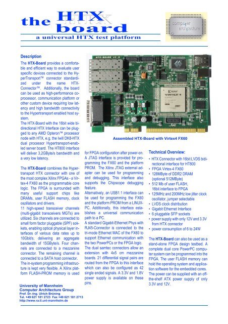
Assembled HTX-Board with Virtex4 FX60<br />
for FPGA configuration after power-on.<br />
A JTAG interface is provided for programming<br />
the FX60 and the platform<br />
PROM. The Xilinx JTAG external adapter<br />
can be used for programming<br />
and debugging. This interface also<br />
supports the Chipscope debugging<br />
feature.<br />
Alternatively, an USB1.1 interface can<br />
be used for programming the FX60<br />
and the platform PROM from a LINUX-<br />
PC. Additionally, this interface establishes<br />
a universal communication<br />
path to a PC.<br />
A standard Gigabit-Ethernet Phys with<br />
RJ45-Connector is connected to the<br />
tri-mode Ethernet MAC of the FX60 to<br />
support Ethernet communication with<br />
the two PowerPCs or the FPGA logic.<br />
The dual samtec connectors allow an<br />
extension with 4x5 cm mezzanine<br />
boards. 21 differential signal pairs are<br />
routed from the FPGA to this interface<br />
which can also be configured as 42<br />
single ended signals. A 3.3V and 1.8V<br />
power supply is available on these<br />
pins.<br />
Technical Overview:<br />
• HTX Connector with 16bit LVDS bidirectional<br />
interface for HT800<br />
• FPGA Virtex-4 FX60<br />
• 128MByte of DDR2 DRAM<br />
(optional 512MByte)<br />
• 512 Mb of user FLASH,<br />
16bit interface to FPGA<br />
• 125MHz and 200MHz low jitter clock<br />
oscillator, jumper selectable<br />
• LVDS clock distribution<br />
• Gigabit Ethernet Interface<br />
• 6 pluggable SFP sockets<br />
• power supply with only 12V and 3.3V<br />
from HTX connector<br />
• power consumption of 6 to 24W<br />
The HTX-Board can also be used as a<br />
stand-alone FPGA design testbed. A<br />
complete dual core PowerPC computer<br />
system can be programmed into the<br />
FPGA. The user FLASH memory can<br />
hold the operating system and application<br />
software for the embedded cores.<br />
The power can be supplied with an offthe-shelf<br />
ATX power supply of only<br />
3.3V and 12V.
the HTX<br />
HTX<br />
board<br />
a universal HTX test platform<br />
Reconfigurable Logic Device<br />
The Xilinx Virtex4 FPGA FX60 or<br />
FX100 in the BGA 1152 ball version<br />
can be assembled on the HTX-Board.<br />
This chip provides a programmable infrastructure<br />
with many features.<br />
The Virtex-4 FX provides a high-performance,<br />
full-featured solution for embedded<br />
platform applications.<br />
FPGA Virtex-4 FX60 features:<br />
• speed grade -10, (-11, -12, on request)<br />
• BGA 1152 with 576 user IOs<br />
• Flip-Chip Packaging, Pb-Free<br />
• Digital Clock Manager (DCM) blocks<br />
• Additional Phase-Matched Clock Dividers<br />
(PMCD)<br />
• Differential Global Clocks<br />
• up to 160 XtremeDSP Slice<br />
• 18x18, two’s complement, signed<br />
Multiplier<br />
• Optional pipeline stages<br />
• Built-In Accumulator (48-bits) &<br />
Adder/Subtracter<br />
• Smart RAM Memory Hierarchy<br />
• Distributed RAM<br />
• up to 376 Dual-Port 18-Kbit RAM<br />
blocks totaling 6,768 Kb of Memory<br />
on chip<br />
• Optional pipeline stages<br />
• Optional programmable FIFO logic<br />
- Automatically remaps RAM<br />
signals as FIFO signals<br />
• High-speed memory interface support:<br />
DDR-2 used on board, up to<br />
512 MByte<br />
• 16 RocketIO MultiGigabit Tranceivers<br />
with SERDES (622Mb/s to<br />
10+Gb/s MGT)<br />
• 2 IBM PowerPC RISC Processor Cores<br />
(PPC405 Core with Auxiliary<br />
Processor Unit Interface) enabling<br />
embedded system solutions<br />
University of Mannheim<br />
<strong>Computer</strong> <strong>Architecture</strong> <strong>Group</strong><br />
Prof. Dr.-Ing. Ulrich Brüning<br />
Tel. +49 621 181 2723 Fax +49 621 181 2713<br />
http://www.ra.ti.uni-mannheim.de<br />
SFP-Transceiver<br />
SFP-Transceiver<br />
SFP-Transceiver<br />
SFP-Transceiver<br />
SFP-Transceiver<br />
Mezzanine Mezzanine<br />
• Tri-Mode Ethernet MAC<br />
• 90-nm copper CMOS process<br />
• 1.2V core voltage<br />
For more details please refer to the Xilinx<br />
Virtex4 FX60/100 user manual.<br />
Assembly options<br />
Many assembly options are possible to<br />
support the board as a versatile test<br />
platform.<br />
The FPGA FX60 can be replaced by a<br />
FX100 providing more internal logic<br />
functions. The FPGA available speed<br />
grades -10, -11, -12) can be used.<br />
The 32bit wide DRAM interface (2x 16<br />
bit word width) can be assembled with<br />
DDR2 DRAMs of various capacities,<br />
starting from 128MB, 256MB to<br />
512MB.<br />
For the user FLASH memory, a 1Gb,<br />
512Mb, 256Mb or 128Mb device can<br />
be assembled.<br />
JTAG<br />
PROM<br />
32MBit<br />
HTX-Connector<br />
Ethernet<br />
PHYS<br />
Blockdiagram of the HTX-Board<br />
USB<br />
Controller<br />
FLASH<br />
Ethernet<br />
Connector<br />
USB<br />
Connector<br />
Clock<br />
Generation<br />
DDR2<br />
4<br />
SFP-Transceiver 4<br />
SATA<br />
HTX<br />
MGT-Mezzanine<br />
PPC<br />
MISC<br />
Xilinx Virtex4-FX60<br />
BGA1152<br />
576 User I/O<br />
12 MGTs<br />
PPC<br />
512MBit<br />
DDR2<br />
266MHz, 512MBiit<br />
266MHz, 512MBiit<br />
Connector<br />
There are two landing pads for LVDS<br />
oszillators which can be selected by<br />
the user. Standard frequencies are<br />
125MHz and 200MHz with a very low<br />
jitter specification as required for the<br />
MGTs. Different LVDS oszillators can<br />
be placed on request.<br />
Instead of 3x SFPs a parallel conncetor<br />
for 2 x 68 pin Honda Connectors<br />
can be assembled providing 2x 40bit of<br />
differential LVDS signal lines. Sufficient<br />
ground lines are supplied to control<br />
the impedance of the connector<br />
and the cable. Compatible cables with<br />
various lengths (1-5m) are available on<br />
request.<br />
Available Soft-Cores<br />
A constraint file in Xilinx .ucf file format<br />
describing the pinout in included.<br />
A HyperTransport core (HT800, 8bit or<br />
16bit wide) is optionally available.
the HTX<br />
HTX<br />
board<br />
a universal HTX test platform<br />
University of Mannheim<br />
<strong>Computer</strong> <strong>Architecture</strong> <strong>Group</strong><br />
Prof. Dr.-Ing. Ulrich Brüning<br />
Tel. +49 621 181 2723 Fax +49 621 181 2713<br />
http://www.ra.ti.uni-mannheim.de<br />
FPGA assembly options with features<br />
Device Logic Cells Block RAM - # of<br />
18Kb Blocks<br />
Additional Options<br />
A HTX-Extender board with test pins<br />
for LSA connection is available in two<br />
versions:<br />
• for the adaption of the HTX signals<br />
with differential flying lead probes<br />
E5381A from Agilent<br />
• a version with build-in probe interface<br />
and direct connection to the Aglient<br />
2x 45 pin 0.05” LSA probe connector<br />
A debug mezzanine board with LEDs,<br />
test pins with 0.1” spacing, differential<br />
flying probe LSA connector and two<br />
SMA coax connectors can be used for<br />
further debugging. A layout file in Cadence<br />
Allegro format can be supplied<br />
to support user specific developments<br />
of mezzanine boards.<br />
DCMs RocketIO Multi Gigabit<br />
Tranceivers<br />
XC4VFX60 56,880 232 12 16 (11 connected) 576<br />
XC4VFX100 94,896 376 12 20 (11 connected) 576<br />
Layout Section of the HTX-Board<br />
All HTX signal traces on the HTX Board are routed as striplines with controlled<br />
impedance and are optimized for equal length, simplifying the HTX interface design.<br />
The board is carefully handrouted with only four interconnect layers.<br />
Max User I/O<br />
About:<br />
<strong>Computer</strong> <strong>Architecture</strong> <strong>Group</strong><br />
The <strong>Computer</strong> <strong>Architecture</strong> <strong>Group</strong> at<br />
the University of Mannheim has the expertise<br />
to design complex hardware/<br />
software systems.<br />
Goals of the applied research activities<br />
are to cover a broad range of methodologies<br />
for the design of complete high<br />
performance systems with the possibility<br />
to optimize every level and educate<br />
students on the various real world topics.<br />
The group mainly focuses on the design<br />
of parallel architectures which<br />
achieve their high performance by improving<br />
communication between computational<br />
devices/units. Scaling such<br />
systems is a great challenge to the architecture<br />
of the interconnection network<br />
(IN) and the network interface<br />
controller (NIC). Special attention is<br />
paid on the interface between software<br />
and hardware to setup communication<br />
instructions.<br />
The HTX-Board is a development of<br />
the University of Mannheim, <strong>Computer</strong><br />
<strong>Architecture</strong> <strong>Group</strong>.