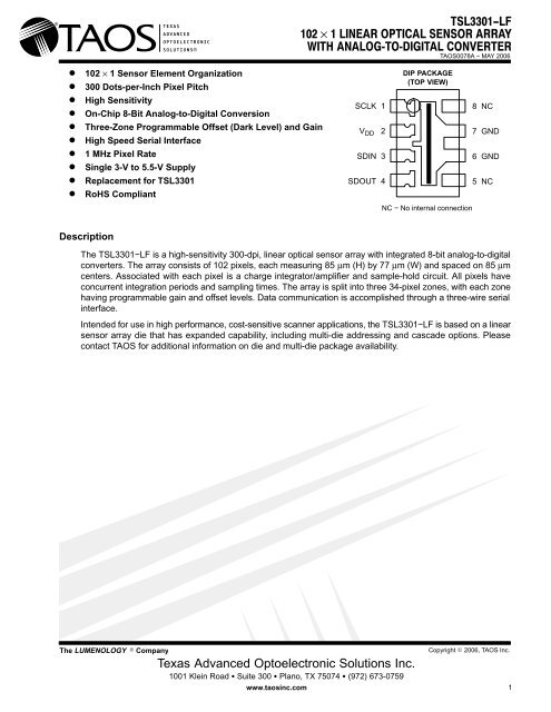
TSL3301−LF 102 × 1 LINEAR OPTICAL SENSOR ARRAY WITH ...
TSL3301−LF 102 × 1 LINEAR OPTICAL SENSOR ARRAY WITH ...
TSL3301−LF 102 × 1 LINEAR OPTICAL SENSOR ARRAY WITH ...

Create successful ePaper yourself
Turn your PDF publications into a flip-book with our unique Google optimized e-Paper software.
<strong>102</strong> <strong>×</strong> 1 Sensor Element Organization<br />
300 Dots-per-Inch Pixel Pitch<br />
High Sensitivity<br />
On-Chip 8-Bit Analog-to-Digital Conversion<br />
Three-Zone Programmable Offset (Dark Level) and Gain<br />
High Speed Serial Interface<br />
1 MHz Pixel Rate<br />
Single 3-V to 5.5-V Supply<br />
Replacement for TSL3301<br />
RoHS Compliant<br />
Description<br />
The LUMENOLOGY Company<br />
<br />
<br />
1001 Klein Road Suite 300 Plano, TX 75074 (972) 673-0759<br />
www.taosinc.com<br />
<strong>TSL3301−LF</strong><br />
<strong>102</strong> <strong>×</strong> 1 <strong>LINEAR</strong> <strong>OPTICAL</strong> <strong>SENSOR</strong> <strong>ARRAY</strong><br />
<strong>WITH</strong> ANALOG-TO-DIGITAL CONVERTER<br />
TAOS0078A − MAY 2006<br />
SCLK 1<br />
V DD 2<br />
SDIN 3<br />
SDOUT 4<br />
The <strong>TSL3301−LF</strong> is a high-sensitivity 300-dpi, linear optical sensor array with integrated 8-bit analog-to-digital<br />
converters. The array consists of <strong>102</strong> pixels, each measuring 85 μm (H) by 77 μm (W) and spaced on 85 μm<br />
centers. Associated with each pixel is a charge integrator/amplifier and sample-hold circuit. All pixels have<br />
concurrent integration periods and sampling times. The array is split into three 34-pixel zones, with each zone<br />
having programmable gain and offset levels. Data communication is accomplished through a three-wire serial<br />
interface.<br />
Intended for use in high performance, cost-sensitive scanner applications, the <strong>TSL3301−LF</strong> is based on a linear<br />
sensor array die that has expanded capability, including multi-die addressing and cascade options. Please<br />
contact TAOS for additional information on die and multi-die package availability.<br />
Texas Advanced Optoelectronic Solutions Inc.<br />
DIP PACKAGE<br />
(TOP VIEW)<br />
NC − No internal connection<br />
8 NC<br />
7 GND<br />
6 GND<br />
5 NC<br />
Copyright 2006, TAOS Inc.<br />
1
<strong>TSL3301−LF</strong><br />
<strong>102</strong> <strong>×</strong> 1 <strong>LINEAR</strong> <strong>OPTICAL</strong> <strong>SENSOR</strong> <strong>ARRAY</strong><br />
<strong>WITH</strong> ANALOG-TO-DIGITAL CONVERTER<br />
TAOS0078A − MAY 2006<br />
Functional Block Diagram<br />
Copyright 2006, TAOS Inc. The LUMENOLOGY Company<br />
<br />
2<br />
SCLK<br />
SDIN<br />
SDOUT<br />
DIGITAL I/O<br />
AND<br />
CONTROL<br />
PIXEL <strong>ARRAY</strong> <strong>WITH</strong> INTEGRATORS AND S−H<br />
(51-bit shift register)<br />
PIXCLK SI HOLD ZERO LEFT ODD<br />
LEFT EVEN RIGHT ODD RIGHT EVEN IREF<br />
8<br />
5<br />
3<br />
DB<br />
ADDR<br />
READ<br />
WRITE<br />
SECTOR<br />
RESET/SAMPLE<br />
START<br />
ADCLK<br />
www.taosinc.com<br />
OUTPUT CHARGE-TO-<br />
VOLTAGE CONVERTER<br />
<strong>WITH</strong> PROGRAMMABLE<br />
GAINS AND OFFSETS<br />
DUAL 8−BIT<br />
SA ADC<br />
<br />
VREF<br />
IREF<br />
VREF<br />
IREF<br />
BIAS<br />
BLOCK
Terminal Functions<br />
TERMINAL<br />
NAME NO.<br />
GND 6, 7 Ground<br />
The LUMENOLOGY Company<br />
I/O DESCRIPTION<br />
SCLK 1 I System clock input for serial I/O and all internal logic.<br />
SDIN 3 I Serial data input. Data is clocked in on the rising edge of SCLK.<br />
SDOUT 4 O Serial data output. Data is clocked out on the falling edge of SCLK.<br />
V DD 2 Positive supply voltage.<br />
Detailed Description<br />
<br />
www.taosinc.com<br />
<strong>TSL3301−LF</strong><br />
<strong>102</strong> <strong>×</strong> 1 <strong>LINEAR</strong> <strong>OPTICAL</strong> <strong>SENSOR</strong> <strong>ARRAY</strong><br />
<strong>WITH</strong> ANALOG-TO-DIGITAL CONVERTER<br />
TAOS0078A − MAY 2006<br />
The <strong>TSL3301−LF</strong> is a <strong>102</strong> <strong>×</strong> 1 linear optical array with onboard A/D conversion. It communicates over a serial<br />
digital interface and operates over a 3 V to 5.5 V range. The array is divided into three 34-pixel zones (left, center,<br />
and right), with each zone having programmable gain and offset (dark signal) correction.<br />
The sensor consists of <strong>102</strong> photodiodes, also called pixels, arranged in a linear array. Light energy impinging<br />
on a pixel generates a photocurrent, which is then integrated by the active integration circuitry associated with<br />
that pixel. During the integration period, a sampling capacitor connects to the output of the integrator through<br />
an analog switch. The amount of charge accumulated at each pixel is directly proportional to the light intensity<br />
(Ee) on that pixel and to the integration time (tint). At maximum programmed gain, one LSB corresponds to<br />
approximately 300 electrons.<br />
Integration, sampling, output, and reset of the integrators are performed by the control logic in response to<br />
commands input via the SDIN pin. Data is read out on the SDOUT pin. A normal sequence of operation consists<br />
of a pixel reset (RESET), start of integration (STARTInt), integration period, sampling of integrators<br />
(SAMPLEInt), and pixel output (READPixel). Reset sets all the integrators to zero. Start of integration releases<br />
the integrators from the reset state and defines the beginning of the integration period. Sampling the integrators<br />
ends the integration period and stores the charge accumulated in each pixel in a sample and hold circuit.<br />
Reading the pixels causes the sampled value of each pixel to be converted to 8-bit digital format and output on<br />
the SDOUT pin. All <strong>102</strong> pixels are output sequentially unless interrupted by an abort (ABORTPixel) command<br />
or reset by a RESET command.<br />
Gain adjustment is controlled by three 5-bit DACs, one for each of the the three zones. Table 1 lists the gain<br />
settings and the corresponding pixel values. Offset is affected by the gain setting and may have to be adjusted<br />
after gain changes are made.<br />
Offset correction is controlled by three 8-bit sign-magnitude † DACs and is performed in the analog domain prior<br />
to the digital conversion. There is a separate offset DAC for each of the three zones. Codes 0h − 7Fh correspond<br />
to positive offset values and codes 80h – FFh correspond to negative offset values.<br />
The offset correction is proportional to the gain setting. At minimal gain, one LSB of the offset DAC corresponds<br />
to approximately 1/3 LSB of the device output, and at maximum gain, to about 1 LSB of the device output.<br />
Note that the gain and offset registers are in indeterminate states after power up and must be set by the controller<br />
as required.<br />
† Sign-magnitude is a binary representation in which the most significant bit (MSB) is used to represent the sign of the number, with the<br />
remaining bits representing the magnitude. An MSB of 1 indicates a negative number.<br />
<br />
Copyright 2006, TAOS Inc.<br />
3
<strong>TSL3301−LF</strong><br />
<strong>102</strong> <strong>×</strong> 1 <strong>LINEAR</strong> <strong>OPTICAL</strong> <strong>SENSOR</strong> <strong>ARRAY</strong><br />
<strong>WITH</strong> ANALOG-TO-DIGITAL CONVERTER<br />
TAOS0078A − MAY 2006<br />
Copyright 2006, TAOS Inc. The LUMENOLOGY Company<br />
<br />
4<br />
Table 1. Gain Settings and Results<br />
GAIN CODE RELATIVE GAIN % INCREASE GAIN CODE RELATIVE GAIN % INCREASE<br />
Serial interface<br />
0 1 16 1.52 3.23<br />
1 1.02 2.17 17 1.57 3.33<br />
2 1.05 2.22 18 1.62 3.45<br />
3 1.07 2.27 19 1.68 3.57<br />
4 1.09 2.33 20 1.74 3.70<br />
5 1.12 2.38 21 1.81 3.85<br />
6 1.15 2.44 22 1.88 4.00<br />
7 1.18 2.50 23 1.96 4.17<br />
8 1.21 2.56 24 2.05 4.35<br />
9 1.24 2.63 25 2.14 4.55<br />
10 1.27 2.70 26 2.24 4.76<br />
11 1.31 2.78 27 2.35 5.00<br />
12 1.34 2.86 28 2.48 5.26<br />
13 1.38 2.94 29 2.61 5.56<br />
14 1.43 3.03 30 2.77 5.88<br />
15 1.47 3.13 31 2.94 6.25<br />
The serial interface follows a USART format, with start bit, 8 data bits, and one or more stop bits. Data is clocked<br />
in synchronously on the rising edge of SCLK and clocked out on the falling edge of SCLK. Stop bits are not<br />
required on the input. When clocking data out continuously (i.e., reading out pixels) there will be one stop bit<br />
between data words.<br />
The receive and transmit state machines are independent, which means commands can be issued while<br />
reading data. This feature allows starting new integration cycles while reading data. Note that this allows<br />
undefined conditions so care must be taken not to issue commands that will cause outputs (such as register<br />
read) while reading out data. For instance, issuing a register read command while reading out image data will<br />
result in garbage out. Likewise, it is possible to change offset and gain registers during a readout, which can<br />
give unpredictable results.<br />
It is not necessary to have a continuously active clock, but a minimum of 5 clocks after the stop bit is required<br />
after any command has been issued to ensure that the corresponding internal logic actions have been<br />
completed. When reading register contents, there will be a 4-clock delay from the completion of the REGRead<br />
command before the register contents are output (see Figure 5). When reading out pixel values, there will be<br />
a 44-clock delay from completion of the READPixel command until the first pixel data is output. When starting<br />
integration (STARTInt), it is necessary to have 22 clocks to complete the pixel reset cycle (see Imaging below).<br />
www.taosinc.com
Register address map<br />
The LUMENOLOGY Company<br />
<br />
www.taosinc.com<br />
<strong>TSL3301−LF</strong><br />
<strong>102</strong> <strong>×</strong> 1 <strong>LINEAR</strong> <strong>OPTICAL</strong> <strong>SENSOR</strong> <strong>ARRAY</strong><br />
<strong>WITH</strong> ANALOG-TO-DIGITAL CONVERTER<br />
TAOS0078A − MAY 2006<br />
The <strong>TSL3301−LF</strong> contains seven registers as defined in Table 2. Data in these registers may be written to or<br />
read from using the REGWrite and REGRead commands. Three registers control the gain of the<br />
analog-to-digital converters (ADC). Three other registers allow the offset of the system to be adjusted. Together<br />
the gain and offset registers are used to maximize the achievable dynamic range.<br />
Table 2. Register Address Map<br />
ADDRESS REGISTER DESCRIPTION REGISTER WIDTH<br />
0x00 Left (pixels 0−33) offset 8<br />
0x01 Left (pixels 0−33) gain 5<br />
0x02 Center (pixels 34−67) offset 8<br />
0x03 Center (pixels 34−67) gain 5<br />
0x04 Right (pixels 68−101) offset 8<br />
0x05 Right (pixels 68−101) gain 5<br />
0x1F Mode 8<br />
The offset registers are 8-bit sign-magnitude values and the gain registers are 5-bit values. The programmed<br />
offset correction is applied to the sampled energy, and then the gain is applied. (i.e., the gain will affect the offset<br />
correction.) These registers allow the user to maximize the dynamic range achievable in the given system.<br />
The last register is the mode register. Bits in this register select the sleep mode as well as options for multichip<br />
arrays and production testing. Note that test and multichip options do not apply to the 8-pin packaged device.<br />
Users should always write zeros into the production test and multichip control bits.<br />
0x1F<br />
SLP = Sleep Mode:<br />
1 places device into sleep mode<br />
7<br />
6 5 4 3 2 1<br />
P2 0 0 SLP P1 P0 C1 C0 MODE<br />
0 places device in normal operating mode<br />
Figure 1. Mode Register Bit Assignments<br />
C1, C0 are Reserved (should be written 0)<br />
P2 to P0 are factory test bits (should be written 0)<br />
<br />
0<br />
Copyright 2006, TAOS Inc.<br />
5
<strong>TSL3301−LF</strong><br />
<strong>102</strong> <strong>×</strong> 1 <strong>LINEAR</strong> <strong>OPTICAL</strong> <strong>SENSOR</strong> <strong>ARRAY</strong><br />
<strong>WITH</strong> ANALOG-TO-DIGITAL CONVERTER<br />
TAOS0078A − MAY 2006<br />
Command description<br />
Copyright 2006, TAOS Inc. The LUMENOLOGY Company<br />
<br />
6<br />
The <strong>TSL3301−LF</strong> is a slave device that reacts strictly to commands received from the digital controller. These<br />
commands cause the device to perform functions such as reset, integrate, sample, etc. Table 3 summarizes<br />
the command types and formats and Table 4 lists the command set for the <strong>TSL3301−LF</strong>. Each command is<br />
described in more detail below.<br />
Table 3. Command Type and Format Summary<br />
COMMAND TYPE FORMAT<br />
Action command < Command byte ><br />
Register write < Command byte > < Data byte ><br />
Table 4. <strong>TSL3301−LF</strong> Command Set<br />
COMMAND DESCRIPTION<br />
IRESET Interface Reset<br />
RESET Reset Integration and read blocks<br />
DETReset Reset determine unique address block<br />
STARTInt Start pixel integration<br />
SAMPLEInt Stop light integration and sample results<br />
READPixel Dump serial the contents of each sampled integrator<br />
ABORTPixel Abort any READPixel operation in progress<br />
READHold Combination of SAMPLEInt and READPixel commands<br />
READHoldNStart Combination of SAMPLEInt, READPixel and STARTInt commands<br />
REGWrite Write a gain, offset, or mode register<br />
REGRead Read a gain, offset, or mode register<br />
www.taosinc.com
The LUMENOLOGY Company<br />
PROGRAMMING INFORMATION<br />
<br />
www.taosinc.com<br />
<strong>TSL3301−LF</strong><br />
<strong>102</strong> <strong>×</strong> 1 <strong>LINEAR</strong> <strong>OPTICAL</strong> <strong>SENSOR</strong> <strong>ARRAY</strong><br />
<strong>WITH</strong> ANALOG-TO-DIGITAL CONVERTER<br />
TAOS0078A − MAY 2006<br />
A minimum of 5 clock cycles after the stop bit is required after any command to ensure that the internal logic<br />
actions have been completed.<br />
Reset Commands<br />
Reset commands are used to put the <strong>TSL3301−LF</strong> into a known state.<br />
IRESET — Interface Initialization<br />
Encoding: Break Character (10 or more consecutive start bits, or zeros)<br />
The commands vary in length from one to three bytes. IRESET initializes the internal state machine that keeps<br />
track of which command bytes have been received. This command should be first and given only once after<br />
power-up to synchronize the <strong>TSL3301−LF</strong> internal command interpreter.<br />
An alternative is to issue three successive RESET commands.<br />
RESET — Main Reset<br />
Encoding: 0x1b: <br />
RESET resets most of the internal control logic of the <strong>TSL3301−LF</strong> and any READPixel command currently in<br />
progress is aborted. RESET puts the pixel integrators into the auto-zero/reset state. Any values that were being<br />
held in the array’s sample/hold circuits are lost.<br />
Pixel Action Commands<br />
NOTE:<br />
The value on the SDOUT pin is not guaranteed from the time power is applied until 30 clocks after<br />
the first RESET command is issued.<br />
Pixel action commands allow the user to control pixel integration and reading of pixel data.<br />
STARTInt — Start Integration<br />
Encoding: 0x08: <br />
STARTInt causes each pixel to leave the reset state and to start integrating light. The actual execution<br />
of STARTInt is delayed 22 clock cycles until the pixel reset cycle has been completed. (See imaging below.)<br />
SAMPLEInt — Stop Integration<br />
Encoding: 0x10: <br />
SAMPLEInt causes each pixel to store its integrator’s contents into a sample and hold circuit. Also, the Integrator<br />
is returned to the reset state.<br />
READPixel — Read Pixel Data<br />
Encoding: 0x02: <br />
READPixel causes the sampled value of each pixel to be converted to an 8-bit digital value that is clocked out<br />
on the SDOUT pin. The LSB is the first data bit, which is preceded by a START bit (logic 0) and followed by a<br />
STOP bit (logic 1). Each pixel in the device is presented on SDOUT starting from pixel 00 and completes with<br />
pixel 101. There is a 44-clock cycle delay from the completion of the READPixel command until the first pixel<br />
data is output.<br />
Gain and offset registers are used to adjust the ADC converter to maximize dynamic range and should be<br />
programmed prior to invoking the READPixel command.<br />
<br />
Copyright 2006, TAOS Inc.<br />
7
<strong>TSL3301−LF</strong><br />
<strong>102</strong> <strong>×</strong> 1 <strong>LINEAR</strong> <strong>OPTICAL</strong> <strong>SENSOR</strong> <strong>ARRAY</strong><br />
<strong>WITH</strong> ANALOG-TO-DIGITAL CONVERTER<br />
TAOS0078A − MAY 2006<br />
ABORTPixel — Abort Pixel Data Read<br />
Copyright 2006, TAOS Inc. The LUMENOLOGY Company<br />
<br />
8<br />
Encoding: 0x19: <br />
ABORTPixel is an optional command that stops a READPixel command during its execution. It also causes pixel<br />
integration to terminate and the device to enter the auto-zero/reset state. Any values that were being held in<br />
the array’s sample/hold circuits are lost.<br />
READHold — Sample and Read Combination<br />
Encoding: 0x12: <br />
READHold is a macro command that combines both the SAMPLEInt and READPixel commands into a single<br />
command.<br />
READHoldNStart Combination<br />
Encoding: 0x16: <br />
READHold is a macro command that combines the SAMPLEInt, READPixel, and StartInt commands into a<br />
single command. 22 clock cycles are necessary to complete the pixel reset cycle.<br />
Register Commands<br />
The register commands provide the user the capability of setting gain and offset corrections for each of the three<br />
zones of pixels. a4−a0 refer to the register address as given in Table 2.<br />
REGWrite — Write a Gain/Offset/Mode Register<br />
Encoding (2 bytes): 0x40 : <br />
REGWrite writes a value into either a gain, offset, or mode register. The 5-bit address of the register is encoded<br />
into the lower 5 bits of the command byte (the first byte). A second byte, which contains the data to be written,<br />
follows the command byte.<br />
REGRead — Read a Gain/Offset/Mode Register<br />
Encoding: 0x60: <br />
REGRead reads the value previously stored in a gain, offset, or mode register. The 5-bit address of the register<br />
is encoded into the lower 5 bits of the command byte. Following receipt of the REGRead command, the device<br />
places the contents of the selected register onto the SDOUT pin, LSB first.<br />
There is a 4-clock cycle delay from the completion of the REGRead command until the register contents are<br />
output.<br />
www.taosinc.com
Initialization Sequence<br />
The LUMENOLOGY Company<br />
<br />
OPERATION<br />
www.taosinc.com<br />
<strong>TSL3301−LF</strong><br />
<strong>102</strong> <strong>×</strong> 1 <strong>LINEAR</strong> <strong>OPTICAL</strong> <strong>SENSOR</strong> <strong>ARRAY</strong><br />
<strong>WITH</strong> ANALOG-TO-DIGITAL CONVERTER<br />
TAOS0078A − MAY 2006<br />
After powering on the device, a minimum of 10 clocks with SDIN held high must be received by the <strong>TSL3301−LF</strong><br />
to clear the receiver logic so that a start bit will be detected correctly. The control logic may then be cleared by<br />
either issuing an IRESET command (break character) or 3 RESET (0x1b) commands. An additional 30 clocks<br />
must be received by the device to assure the state of SDOUT.<br />
Sleep Mode<br />
The device can be put into a power down or sleep mode by writing a 0x10 to the mode register. This turns off<br />
all the analog circuitry on the chip. Normal operation is restored by writing a 0x00 to the mode register. The<br />
analog circuitry will require a minimum of 1 millisecond to recover from the sleep mode. †<br />
Note that putting the device in the sleep mode does not affect the logic states of the machine. If, for example,<br />
a READPixel command is issued, the device will respond but the resulting data will be meaningless. Also note<br />
that 0x00 and 0x40 are the only two legitimate user programmable values for the single-chip version of the<br />
<strong>TSL3301−LF</strong>. Other values may put the device into a non-operational mode.<br />
† For minimum sleep mode current consumption, voltage levels on logic inputs must be at either VDD or ground.<br />
Imaging<br />
After powering up the device and completing the initialization sequence, it is necessary to allow a minimum of<br />
1 millisecond for the internal analog circuitry to settle. This delay is also required when coming out of the sleep<br />
mode.<br />
Issuing a STARInt (0x08) command will release the pixel integrators from the reset state. After an appropriate<br />
delay to integrate the image, the pixel data may be sampled by issuing a SAMPLEInt (0x10) command and then<br />
read out by issuing a READPixel (0x02) command.<br />
A STARTInt command can be issued anytime after the SAMPLEInt command is issued to start another cycle.<br />
Thus, it is possible to be reading out one sample while integrating the next. However, the sampled data from<br />
the previous SAMPLEInt must be completely read out before the next SAMPLEInt command is issued.<br />
The compound commands READHold (0x12) and READHoldNStart ((0x16) are shortcut commands to simplify<br />
the imaging sequence.<br />
It is important to note that a pixel reset sequence is initiated with the receipt of a STARTInt or READHoldNStart<br />
command. The next integration sequence cannot start until the pixel reset sequence has been completed, which<br />
requires 22 clocks AFTER the receipt of one of these commands. These clocks can also be used to clock<br />
commands or data into or out of the device.<br />
<br />
Copyright 2006, TAOS Inc.<br />
9
<strong>TSL3301−LF</strong><br />
<strong>102</strong> <strong>×</strong> 1 <strong>LINEAR</strong> <strong>OPTICAL</strong> <strong>SENSOR</strong> <strong>ARRAY</strong><br />
<strong>WITH</strong> ANALOG-TO-DIGITAL CONVERTER<br />
TAOS0078A − MAY 2006<br />
Absolute Maximum Ratings over operating free-air temperature (unless otherwise noted) †<br />
Copyright 2006, TAOS Inc. The LUMENOLOGY Company<br />
<br />
10<br />
Supply voltage, VDD . . . . . . . . . . . . . . . . . . . . . . . . . . . . . . . . . . . . . . . . . . . . . . . . . . . . . . . . . . . . . . . . . . . . . . . . 6 V<br />
Digital output voltage range, VO . . . . . . . . . . . . . . . . . . . . . . . . . . . . . . . . . . . . . . . . . . . . . . . −0.3 V to VDD +0.3 V<br />
Digital output current . . . . . . . . . . . . . . . . . . . . . . . . . . . . . . . . . . . . . . . . . . . . . . . . . . . . . . . . . . . . . . −10 to +10 mA<br />
Digital input current range, II . . . . . . . . . . . . . . . . . . . . . . . . . . . . . . . . . . . . . . . . . . . . . . . . . . . . . −20 mA to 20 mA<br />
Operating free-air temperature range, TA . . . . . . . . . . . . . . . . . . . . . . . . . . . . . . . . . . . . . . . . . . . . −25°C to 85°C<br />
Storage temperature range . . . . . . . . . . . . . . . . . . . . . . . . . . . . . . . . . . . . . . . . . . . . . . . . . . . . . . . . −25C to 85C<br />
Lead temperature 1,6 mm (1/16 inch) from case for 10 seconds ‡ . . . . . . . . . . . . . . . . . . . . . . . . . . . . . . . 260°C<br />
ESD tolerance, human body model . . . . . . . . . . . . . . . . . . . . . . . . . . . . . . . . . . . . . . . . . . . . . . . . . . . . . . . . 2000 V<br />
† Stresses beyond those listed under “absolute maximum ratings” may cause permanent damage to the device. These are stress ratings only, and<br />
functional operation of the device at these or any other conditions beyond those indicated under “recommended operating conditions” is not<br />
implied. Exposure to absolute-maximum-rated conditions for extended periods may affect device reliability.<br />
‡ Not recommended for solder reflow.<br />
Recommended Operating Conditions<br />
MIN NOM MAX UNIT<br />
Supply voltage, VDD 3 5 5.5 V<br />
High-level input voltage at SCLK, SDIN, VIH 2 VDD V<br />
Low-level input voltage at SCLK, SDIN, VIL 0.8 V<br />
Power supply ripple, 100 kHz sawtooth waveform 60 mVp-p<br />
Input clock (SCLK) rise time, 10% to 90% 30 ns<br />
Operating junction temperature, TJ 0 70 °C<br />
Maximum clock frequency, f SCLK 10 MHz<br />
Electrical Characteristics over recommended operating free-air temperature range (unless<br />
otherwise noted)<br />
PARAMETER TEST CONDITIONS MIN TYP MAX UNIT<br />
V VOH High High-level level output voltage voltage, SDOUT<br />
V VDD = 5V 5 V<br />
V VDD = 33V 3.3 V<br />
IO = 50 μA<br />
IO = 4 mA<br />
IO = 50 μA<br />
IO = 4 mA<br />
4.5 4.95<br />
4.6<br />
2.9<br />
2.7<br />
V<br />
V VOL Low Low-level level output voltage voltage, SDOUT<br />
www.taosinc.com<br />
I O = 50 μA 0.01 0.1<br />
I O = 4 mA 0.4<br />
A/D active 11 17<br />
I DD Supply Su ly current<br />
A/D inactive 6 11<br />
<br />
V<br />
mA<br />
Sleep mode 10 μΑ<br />
V IL Low-level input voltage (SCLK, SDIN) 0.8 V<br />
V IH High-level input voltage (SCLK, SDIN) 2 V<br />
I IH High-level input current (SCLK, SDIN) V I = V DD ±10 μΑ<br />
I IL Low-level input current (SCLK, SDIN) V I = 0 ±10 μΑ
The LUMENOLOGY Company<br />
<br />
www.taosinc.com<br />
<strong>TSL3301−LF</strong><br />
<strong>102</strong> <strong>×</strong> 1 <strong>LINEAR</strong> <strong>OPTICAL</strong> <strong>SENSOR</strong> <strong>ARRAY</strong><br />
<strong>WITH</strong> ANALOG-TO-DIGITAL CONVERTER<br />
TAOS0078A − MAY 2006<br />
Light-to-Digital Transfer Characteristics at V DD = 5 V, T J = 25°C, λ p = 660 nm, t int = 250 μs (unless<br />
otherwise noted)<br />
PARAMETER TEST CONDITIONS MIN TYP MAX UNIT<br />
A-to-D converter resolution 8 Bits<br />
Full Full-scale scale reference<br />
Full-scale reference temperature sensitivity<br />
Average dark dark-level level offset<br />
Dark signal nonuniformity (DSNU)<br />
Average white level output<br />
Gain register = 00000b 3.6<br />
Gain register = 11111b 1.24<br />
Gain register = 00000b<br />
Gain register = 11111b<br />
Offset register =<br />
For converter only, does not include<br />
photodiode characteristics<br />
Offset register = 00000000b<br />
00000000b Gain register = 11111b<br />
Ee = 3.77 μW/cm 2<br />
<br />
nJ/cm2 nJ/cm2 ±150 ppm/°C<br />
0 7 30<br />
Gain register = 00000b, see Note 1 5 10<br />
Gain register = 11111b, see Note 1 14<br />
Gain register = 00000b<br />
Ee = 11.3 μW/cm 2 160 200 240<br />
Photo-response non-uniformity (PRNU) Ee = 11.3 μW/cm 2 , See Notes 2 and 3 ±4% ±5%<br />
Programmable offset steps ±128<br />
Programmable offset step size<br />
Gain register = 00000b 0.5<br />
Gain register = 11111b 1.5<br />
Dark-level change with temperature 0°C < T J < 70°C 2 LSB<br />
Differential nonlinearity ±0.5 LSB<br />
Integral nonlinearity ±1 LSB<br />
Dark level noise<br />
Gain register = 00000b 0.5<br />
Gain register = 11111b 1.5<br />
NOTES: 1. DSNU is the difference between the highest value pixel and the lowest value pixel of the device under test when the array is not<br />
illuminated.<br />
2. PRNU does not include DSNU.<br />
3. PRNU is the difference between the highest value pixel and the lowest value pixel of the device under test when the array is uniformly<br />
illuminated at nominal white level (typical average output level = 200).<br />
Timing Requirements over recommended operating range (unless otherwise noted) (Figure 2)<br />
MIN NOM MAX UNIT<br />
fmax Maximum clock frequency 10 MHz<br />
tw(CLKH) Clock high pulse duration 30 ns<br />
tw(CLKL) Clock low pulse duration 30 ns<br />
tsu Input setup time 20 ns<br />
th Input hold time 20 ns<br />
Switching Characteristics over recommended operating range (unless otherwise noted) (Figure 3)<br />
t r<br />
t f<br />
Rise time, output<br />
Fall time, output<br />
20<br />
200<br />
LSB<br />
LSB<br />
LSB<br />
LSB<br />
LSB<br />
PARAMETER TEST CONDITIONS MIN TYP MAX UNIT<br />
C CL = 20 pF<br />
10 ns<br />
10 ns<br />
t d Delay from clock edge to data-out stable 20 ns<br />
C i Input pin capacitance 10 pF<br />
Copyright 2006, TAOS Inc.<br />
11
<strong>TSL3301−LF</strong><br />
<strong>102</strong> <strong>×</strong> 1 <strong>LINEAR</strong> <strong>OPTICAL</strong> <strong>SENSOR</strong> <strong>ARRAY</strong><br />
<strong>WITH</strong> ANALOG-TO-DIGITAL CONVERTER<br />
TAOS0078A − MAY 2006<br />
Copyright 2006, TAOS Inc. The LUMENOLOGY Company<br />
<br />
12<br />
SCLK<br />
SDIN<br />
SCLK<br />
SDOUT<br />
Start<br />
SCLK<br />
SDIN<br />
TYPICAL CHARACTERISTICS<br />
t su<br />
t w(CLKH)<br />
t h<br />
www.taosinc.com<br />
t w(CLKL)<br />
<br />
V IH<br />
V IL<br />
V IH<br />
Figure 2. <strong>TSL3301−LF</strong> Input Timing Requirements<br />
SCLK<br />
SDOUT<br />
t d<br />
V IH<br />
V IL<br />
V OH<br />
V OL<br />
Figure 3. <strong>TSL3301−LF</strong> Output Switching Characteristics<br />
B0 B1 B2 B3 B4 B5 B6 B7 Stop<br />
Start<br />
Serial Input Data Format<br />
B0 B1 B2 B3 B4 B5 B6 B7 Stop<br />
Serial Output Data Format<br />
Figure 4. <strong>TSL3301−LF</strong> Serial I/O<br />
V IL
SCLK<br />
SDIN<br />
SDOUT<br />
The LUMENOLOGY Company<br />
B7 Stop<br />
TYPICAL CHARACTERISTICS<br />
END of REGRead Command<br />
<br />
www.taosinc.com<br />
<strong>TSL3301−LF</strong><br />
<strong>102</strong> <strong>×</strong> 1 <strong>LINEAR</strong> <strong>OPTICAL</strong> <strong>SENSOR</strong> <strong>ARRAY</strong><br />
<strong>WITH</strong> ANALOG-TO-DIGITAL CONVERTER<br />
TAOS0078A − MAY 2006<br />
1 2 3 4<br />
Start<br />
<br />
B0<br />
Beginning of Output Response<br />
Figure 5. <strong>TSL3301−LF</strong> REGRead Output Response Timing<br />
Relative Responsivity<br />
1.2<br />
1.0<br />
0.8<br />
0.6<br />
0.4<br />
0.2<br />
PHOTODIODE SPECTRAL RESPONSIVITY<br />
T A = 25°C<br />
0<br />
300 500 700<br />
λ − Wavelength − nm<br />
900<br />
Normalized to<br />
660 nm<br />
1100<br />
Figure 6. <strong>TSL3301−LF</strong> Photodiode Spectral Response<br />
Copyright 2006, TAOS Inc.<br />
13
<strong>TSL3301−LF</strong><br />
<strong>102</strong> <strong>×</strong> 1 <strong>LINEAR</strong> <strong>OPTICAL</strong> <strong>SENSOR</strong> <strong>ARRAY</strong><br />
<strong>WITH</strong> ANALOG-TO-DIGITAL CONVERTER<br />
TAOS0078A − MAY 2006<br />
Normal Sequence<br />
Copyright 2006, TAOS Inc. The LUMENOLOGY Company<br />
<br />
14<br />
APPLICATION INFORMATION<br />
A typical programming sequence for the <strong>TSL3301−LF</strong> device appears below:<br />
Send(IRESET);<br />
Send(RESET);<br />
Calibration Cycle<br />
*<br />
*<br />
while(1) {<br />
for(i=0;i
The LUMENOLOGY Company<br />
MECHANICAL INFORMATION<br />
<br />
www.taosinc.com<br />
<strong>TSL3301−LF</strong><br />
<strong>102</strong> <strong>×</strong> 1 <strong>LINEAR</strong> <strong>OPTICAL</strong> <strong>SENSOR</strong> <strong>ARRAY</strong><br />
<strong>WITH</strong> ANALOG-TO-DIGITAL CONVERTER<br />
TAOS0078A − MAY 2006<br />
This dual-in-line package consists of an integrated circuit mounted on a lead frame and encapsulated in an electrically<br />
nonconductive clear plastic compound.<br />
0.310 (7,87)<br />
0.290 (7,37)<br />
0.075 (1,91)<br />
0.060 (1,52)<br />
Pixel 1 CL 100°<br />
90°<br />
10°<br />
8°<br />
450 m Typical<br />
C L<br />
Pin 1<br />
Centerline of Pin 1 Nominally<br />
Lies Between Pixels 5 and 6.<br />
0.260 (6,60)<br />
0.240 (6,10)<br />
0.130 (3,30)<br />
0.120 (3,05)<br />
0.012 (0,30)<br />
0.008 (0,20)<br />
0.260 (6,60)<br />
0.240 (6,10)<br />
0.03 (0,76) NOM<br />
Seating Plane<br />
NOTES: A. All linear dimensions are in inches and (millimeters).<br />
B. Index of refraction of clear plastic is 1.55.<br />
C. Center of pixel active areas typically located under this line.<br />
D. Lead finish is NiPd.<br />
E. This drawing is subject to change without notice.<br />
1<br />
8<br />
C L Pin 1<br />
0.016 (0,41)<br />
0.014 (0,36)<br />
Die Thickness<br />
0.060 (1,52)<br />
0.040 (1,02)<br />
Figure 7. Packaging Configuration<br />
0.440 (11,18)<br />
0.420 (10,67)<br />
<br />
C<br />
7 L<br />
6<br />
2 3<br />
0.10 (2,54)<br />
5<br />
4<br />
0.025 (0,64)<br />
0.015 (0,38)<br />
8°<br />
8°<br />
0.150 (3,81)<br />
0.125 (3,18)<br />
0.017 (0,43)<br />
0.004 (0,1)<br />
Pixel Coverage<br />
(Note C)<br />
C L Package<br />
0.053 (1,35)<br />
0.043 (1,09)<br />
0.175 (4,45)<br />
0.155 (3,94)<br />
Pb<br />
Copyright 2006, TAOS Inc.<br />
15
<strong>TSL3301−LF</strong><br />
<strong>102</strong> <strong>×</strong> 1 <strong>LINEAR</strong> <strong>OPTICAL</strong> <strong>SENSOR</strong> <strong>ARRAY</strong><br />
<strong>WITH</strong> ANALOG-TO-DIGITAL CONVERTER<br />
TAOS0078A − MAY 2006<br />
Copyright 2006, TAOS Inc. The LUMENOLOGY Company<br />
<br />
16<br />
PRODUCTION DATA — information in this document is current at publication date. Products conform to<br />
specifications in accordance with the terms of Texas Advanced Optoelectronic Solutions, Inc. standard<br />
warranty. Production processing does not necessarily include testing of all parameters.<br />
LEAD-FREE (Pb-FREE) and GREEN STATEMENT<br />
Pb-Free (RoHS) TAOS’ terms Lead-Free or Pb-Free mean semiconductor products that are compatible with the current<br />
RoHS requirements for all 6 substances, including the requirement that lead not exceed 0.1% by weight in homogeneous<br />
materials. Where designed to be soldered at high temperatures, TAOS Pb-Free products are suitable for use in specified<br />
lead-free processes.<br />
Green (RoHS & no Sb/Br) TAOS defines Green to mean Pb-Free (RoHS compatible), and free of Bromine (Br) and<br />
Antimony (Sb) based flame retardants (Br or Sb do not exceed 0.1% by weight in homogeneous material).<br />
Important Information and Disclaimer The information provided in this statement represents TAOS’ knowledge and<br />
belief as of the date that it is provided. TAOS bases its knowledge and belief on information provided by third parties,<br />
and makes no representation or warranty as to the accuracy of such information. Efforts are underway to better integrate<br />
information from third parties. TAOS has taken and continues to take reasonable steps to provide representative<br />
and accurate information but may not have conducted destructive testing or chemical analysis on incoming materials and<br />
chemicals. TAOS and TAOS suppliers consider certain information to be proprietary, and thus CAS numbers and other<br />
limited information may not be available for release.<br />
NOTICE<br />
Texas Advanced Optoelectronic Solutions, Inc. (TAOS) reserves the right to make changes to the products contained in this<br />
document to improve performance or for any other purpose, or to discontinue them without notice. Customers are advised<br />
to contact TAOS to obtain the latest product information before placing orders or designing TAOS products into systems.<br />
TAOS assumes no responsibility for the use of any products or circuits described in this document or customer product<br />
design, conveys no license, either expressed or implied, under any patent or other right, and makes no representation that<br />
the circuits are free of patent infringement. TAOS further makes no claim as to the suitability of its products for any particular<br />
purpose, nor does TAOS assume any liability arising out of the use of any product or circuit, and specifically disclaims any<br />
and all liability, including without limitation consequential or incidental damages.<br />
TEXAS ADVANCED OPTOELECTRONIC SOLUTIONS, INC. PRODUCTS ARE NOT DESIGNED OR INTENDED FOR<br />
USE IN CRITICAL APPLICATIONS IN WHICH THE FAILURE OR MALFUNCTION OF THE TAOS PRODUCT MAY<br />
RESULT IN PERSONAL INJURY OR DEATH. USE OF TAOS PRODUCTS IN LIFE SUPPORT SYSTEMS IS EXPRESSLY<br />
UNAUTHORIZED AND ANY SUCH USE BY A CUSTOMER IS COMPLETELY AT THE CUSTOMER’S RISK.<br />
LUMENOLOGY, TAOS, the TAOS logo, and Texas Advanced Optoelectronic Solutions are registered trademarks of Texas Advanced<br />
Optoelectronic Solutions Incorporated.<br />
www.taosinc.com