Download - ECS EPrints Repository
Download - ECS EPrints Repository
Download - ECS EPrints Repository

You also want an ePaper? Increase the reach of your titles
YUMPU automatically turns print PDFs into web optimized ePapers that Google loves.
Charge injection and trapping in silicon nanocrystals<br />
M. A. Rafiq<br />
Microelectronics Research Centre, Cavendish Laboratory, University of Cambridge, Madingley Road,<br />
Cambridge CB3 0HE, United Kingdom<br />
Y. Tsuchiya, H. Mizuta, and S. Oda<br />
Department of Physical Electronics, Tokyo Institute of Technology, O-Okayama, Meguro-ku,<br />
Tokyo 152-8552, Japan and SORST Japan Science and Technology, Japan<br />
Shigeyasu Uno<br />
Hitachi Cambridge Laboratory, Cavendish Laboratory, Madingley Road, Cambridge CB3 0HE,<br />
United Kingdom<br />
Z. A. K. Durrani a and W. I. Milne<br />
Electronic Devices and Materials Group, Engineering Department, University of Cambridge, Trumpington<br />
Street, Cambridge CB2 1PZ, United Kingdom and SORST Japan Science and Technology, Japan<br />
Received 28 March 2005; accepted 21 September 2005; published online 24 October 2005<br />
The temperature dependence of the conduction mechanism in thin films of 8 nm diameter silicon<br />
nanocrystals is investigated using Al/Si nanocrystal/ p-Si/Al diodes. A film thickness of 300 nm is<br />
used. From 300 to 200 K, space charge limited current, in the presence of an exponential distribution<br />
of trapping states, dominates the conduction mechanism. Using this model, a trap density Nt=2.3 1017 cm−3 and a characteristic trap temperature Tt=1670 K can be extracted. The trap density is<br />
within an order of magnitude of the nanocrystal number density, suggesting that most nanocrystals<br />
trap single or a few carriers at most. © 2005 American Institute of Physics.<br />
DOI: 10.1063/1.2119431<br />
In recent years, there has been great interest in silicon<br />
nanocrystals prepared by various growth techniques. 1–4 The<br />
nanometer-scale size of these crystals leads to novel electronic<br />
and optical properties associated with quantum confinement<br />
and single-electron charging effects. These properties<br />
have been exploited for the fabrication of single-electron<br />
transistors and memories, 1,5 electron emitters, 6 and silicon<br />
light emitting devices. 7 The possibility of precise control of<br />
the nanocrystal size and separation, e.g., by plasma decomposition<br />
of SiH 4, 3,7 raises the possibility of large numbers of<br />
nanocrystal devices with well defined electrical and optical<br />
characteristics.<br />
At present, there are only limited investigations of the<br />
macroscopic electronic conduction mechanism across Si<br />
nanocrystal films. While electronic transport through single<br />
nanocrystals shows strong single-electron charging effects at<br />
low temperatures, 8 it is not clear if this occurs in large numbers<br />
of nanocrystals. At high bias, it is possible to observe<br />
electron emission from thin films of nanocrystals. 6 In investigations<br />
of the electrical and electroluminescence characteristics<br />
of Si nanocrystals prepared by pulsed laser ablation, a<br />
space charge limited current 9 SCLC and tunneling conduction<br />
mechanism has been suggested. 10 In contrast, there are<br />
detailed investigations of carrier transport in porous Si films<br />
which may contain silicon nanocrystals, and in other systems<br />
such as CdSe nanocrystals, where SCLC electron transport<br />
has been demonstrated explicitly. 11–14<br />
This letter investigates the macroscopic electronic conduction<br />
mechanism across 300-nm-thick Si nanocrystal films<br />
with 8 nm diameter nanocrystals. We measure the temperature<br />
dependence of the I-V characteristics of<br />
Al/Si nanocrystal/ p-Si/Al diodes from 300 to 40 K. From<br />
a Electronic mail: zakd100@cam.ac.uk<br />
APPLIED PHYSICS LETTERS 87, 182101 2005<br />
300 to 200 K, the conduction mechanism is dominated by<br />
SCLC transport, in the presence of an exponential distribution<br />
of trapping states. Using this model, we extract a trap<br />
density N t=2.310 17 cm −3 and a characteristic trap temperature<br />
T t=1670 K. The trap density was within an order of<br />
magnitude of the nanocrystal number density, suggesting that<br />
most nanocrystals trap single or a few carriers at most.<br />
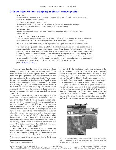
Figure 1a shows a schematic diagram of our device.<br />
The device uses a 300 nm thick Si nanocrystal film, deposited<br />
by plasma decomposition of SiH 4 Ref. 1 on a p-Si<br />
substrate resistivity: 10 cm. The nanocrystals are<br />
8 nm±1 nm in diameter and undoped, with a 1.5-nm-thick<br />
surface SiO 2 layer, at least for nanocrystals near the film<br />
surface. Figure 1b shows a scanning electron micrograph of<br />
FIG. 1. a Schematic of the Al/Si nanocrystal/ p-Si/Al diode. b Scanning<br />
electron micrograph of the Si nanocrystal film. c. Transmission electron<br />
micrograph of a Si nanocrystal.<br />
0003-6951/2005/8718/182101/3/$22.50 © 2005 American Institute of Physics<br />
87, 182101-1<br />
<strong>Download</strong>ed 21 Jul 2008 to 152.78.61.227. Redistribution subject to AIP license or copyright; see http://apl.aip.org/apl/copyright.jsp
182101-2 Rafiq et al. Appl. Phys. Lett. 87, 182101 2005<br />
FIG. 2. a I-V characteristics of a 35 m35 m diode from 300 to 40 K,<br />
on a log-log plot. The temperature step is 20 K. The inset shows the I-V<br />
characteristics at 300 K, from −8 to 4 V, on a linear scale. b Schematic<br />
diagram of SCLC transport. The SiO 2 potential barriers in the Si nanocrystal<br />
film are omitted for clarity. Carriers holes are injected from the p-Si substrate<br />
into the film. An exponential distribution of traps n t(E) exists in the<br />
film.<br />
our film. Figure 1c shows a transmission electron micrograph<br />
of a nanocrystal with 3 nm oxide due to thermal<br />
processing 1 h oxidation before microscopy. The film is<br />
nonuniform, with a nanocrystal coverage 60% per layer<br />
and a number density, Nnc1.21018 /cm3 . Our film thickness<br />
of 300 nm avoids pinholes across the film. The diodes<br />
were defined using “mesas”, fabricated by electron-beam lithography<br />
and reactive ion etching. A 150-nm-thick sputtered<br />
SiO2 layer, wet-etched over the mesa to expose the<br />
nanocrystals, was used to support an Al top contact. The<br />
substrate contact was also in Al. The diode area, determined<br />
by the top Al–Si nanocrystal contact area, was varied from<br />
35 m35 m to 200 m200 m. The diode current is<br />
seen to scale with device area.<br />
The I-V characteristics of a 35 m35 m diode from<br />
300 to 40 K, measured using a cryogenic temperature needle<br />
prober BCT-43MDC, Nagase & Co. Ltd. and a Hewlett<br />
Packard 4156A parameter analyzer, are shown in Fig. 2a on<br />
a log-log plot. The inset shows the room temperature I-V<br />
characteristics of the device from −8 to 4 V linear scale.<br />
Here, positive bias is applied to the substrate contact, corresponding<br />
to a forward biased substrate. The I-V characteristics<br />
are asymmetric with voltage Fig. 2a, inset. The rectifying<br />
ratio at room temperature, IF/I R=450 at V=2.5 V,<br />
and the turn-on voltages for forward and reverse bias are<br />
VF0.9 V and VR−6 V, respectively. We note that the<br />
I-V characteristic between two substrate contacts is linear at<br />
300 K, with a substrate contact resistance 100 k. The<br />
rectifying nature of the I-V characteristics of our device is<br />
then due to the p-Si/Si nanocrystal/top Al layers. The total<br />
resistance at 300 K of the device is 430 k, above VF. This includes the 100 k substrate-contact resistance.<br />
At 300 K, the current above a voltage threshold 1.2 V<br />
increases along a straight line in our log-log plot, corresponding<br />
to an IV m dependence, where m1.8. This behavior<br />
persists to 200 K, but with increasing m from 1.8<br />
to 4, and increasing voltage threshold, from 1.2 to 4 V.<br />
The increase in m leads to convergence of the I-V characteristics<br />
from 300 to 200 K, such that the different curves can<br />
be extrapolated to meet at a single point see Fig. 3. Below<br />
200 K, the curves do not converge towards a single point,<br />
FIG. 3. Power law fits to the data of Fig. 2 from 280 to 200 K, with a<br />
temperature step of 20 K. The fits meet at cross over voltage V c=17 V. The<br />
inset shows m as a function of inverse temperature.<br />
and instead tend to a constant slope. For low voltages, e.g.,<br />
below 1.2 V at 300 K, the current can be shown to increase<br />
exponentially. In order to confirm that the behavior of Fig.<br />
2a is due to the Si nanocrystal layer and not due to the p-Si<br />
substrate, we have also measured the temperature dependence<br />
of the I-V characteristics between two Al substrate<br />
contacts, from 300 to 40 K. These curves show an exponential<br />
I-V dependence and do not show the dependence<br />
of Fig. 2a. The current in these curves also remains larger<br />
than in Fig. 2a, implying that in our Al/Si nanocrystal/p-<br />
Si/Al structure, there is a lower resistance for the<br />
p-Si substrate/Al substrate-contact part than for the top<br />
Al contact/Si nanocrystal part. Therefore, the dependence<br />
of Fig. 2a can be associated with the top<br />
Al contact/nanocrystal film.<br />
The characteristics from 300 to 200 K can be explained<br />
using a SCLC model with an exponential density of traps. 9,15<br />
Our free carriers are injected from the substrate into transport<br />
states in the film Fig. 2b. An exponential distribution of<br />
traps above these states reduces the number of free carriers.<br />
With increasing voltage, the Fermi level fall through the distribution,<br />
filling the traps and causing a rapid increase in free<br />
carriers. Assuming a constant mobility, a free carrier concentration<br />
much less than the trapped carrier concentration, an<br />
exponential trap distribution, and considering only majority<br />
carriers in our case, holes from the substrate, the current<br />
density is 15<br />
J = q1−l l+1<br />
2l +1<br />
pNv l +1<br />
l<br />
l +1<br />
l l+1<br />
s0 V 2l+1 . 1<br />
Nt d<br />
Here, N t is the trap density, 0 is the permittivity of free<br />
space, s the dielectric constant, p is the hole mobility, N v is<br />
the density of transport states, d is the sample thickness, and<br />
l=T t/T, where T is the measurement temperature and T t is<br />
the characteristic temperature. T t is related to the characteristic<br />
energy of the trap distribution, E t=k BT t, where k B is the<br />
Boltzmann constant. Equation 1 predicts a J-V m dependence,<br />
where m=l+1. Thus, the slope of a log-log plot of<br />
J-V directly determines the characteristic temperature and<br />
energy.<br />
Figure 3 shows SCLC power law fits to the data of Fig.<br />
2a from 280 to 200 K, where the data converges to V c<br />
=17 V and the slopes give the exponent m. The inset shows<br />
that m increases linearly as a function of inverse temperature,<br />
as predicted by SCLC theory. Here, T t=1670 K, and E t<br />
=0.14 eV. Below 200 K, the curves tend to a constant m<br />
and the SCLC model does not fit. This is because the thermal<br />
<strong>Download</strong>ed 21 Jul 2008 to 152.78.61.227. Redistribution subject to AIP license or copyright; see http://apl.aip.org/apl/copyright.jsp
182101-3 Rafiq et al. Appl. Phys. Lett. 87, 182101 2005<br />
energy is not sufficient to ionize carriers between the traps<br />
and the transport states. Carrier transport at these temperatures<br />
can occur by hopping conduction. 11,16 In our data at<br />
low temperature, the conductance can be shown to follow a<br />
T−1/2 law, corresponding to variable range hopping with Coulomb<br />
interactions. 17<br />
Equation 1 can be approximated in an Arrenhius<br />
form 18<br />
J = 1<br />
2 pNvqVexp− d Et kT ln qNtd2 2<br />
2s0V, where the activation energy is<br />
Ea = Et k ln qNtd2 3<br />
2s0V. This relates the slope of the ln(J) vs 1/T curves at constant<br />
voltage to the total trap density. An examination of Eq. 2<br />
shows that the current is temperature independent at a<br />
“crossover voltage” Vc, where Ea=0 and<br />
Vc = qNtd2 . 4<br />
2s0 If the curves of Fig. 2a from 300 to 200 K are extrapolated,<br />
then it is possible to obtain the crossover voltage Vc. Figure<br />
3 shows this data, with IV m fits to the data solid lines<br />
extrapolated to find Vc. Here, Vc=17 V, which gives Nt =2.31017 cm−3 . In addition, if we plot our data in an Arrenhius<br />
plot lnI vs 1/T, we can directly measure Ea 200 meV at a bias of 4 V. This gives Nt=2.41017 cm−3 Eq. 3, which is close to Nt determined from the crossover<br />
voltage Eq. 4.<br />
Our value of Nt is very similar to the nanocrystal number<br />
density, Nnc1.21018 cm−3 . This suggests that only a few<br />
carriers are trapped per nanocrystal. With SCLC, holes are<br />
injected from the substrate into the nanocrystal film. A potential<br />
well may exist on each nanocrystal, between potential<br />
barriers at the nanocrystal surface. Single-electron or quantum<br />
confinement effects could then lead to a discrete density<br />
of states in the well. 4,8 If the higher charge number states,<br />
closer to the top of the potential barrier, were delocalized<br />
then only a few localized trapping states would exist on a<br />
nanocrystal. This would limit the number of carriers trapped<br />
in the well and explain our similarity between Nt and Nnc. Alternatively, the trapping states may be formed by only a<br />
small number of defect states per nanocrystal.<br />
The values of Tt=1670 K corresponding to Et =0.14 eV and Nt=2.31017 cm−3 can be compared to<br />
amorphous Si and to other nanocrystal systems. Tt does not<br />
lie in the range observed for bulk amorphous Si 300–<br />
1300 K or for large 150 nm amorphous Si nanoparticles,<br />
and Nt is two orders of magnitude smaller than in<br />
amorphous Si. 19,20 Our values of T t and N t are more comparable<br />
to values observed in CdSe nanocrystals, similar in size<br />
to our Si nanocrystals, In CdSe, T t1750 K, E t=0.15 eV,<br />
and N t10 16 –10 17 cm −3 . 13,14 We speculate that our traps<br />
may be associated with nanocrystal size. Our ratio N nc/N t<br />
5 is lower than in CdSe nanocrystals, where a ratio of 100<br />
was observed for deep level traps. 14 This suggests more uniform<br />
charging in our Si nanocrystals films.<br />
In conclusion, we investigated the conduction mechanism<br />
in 300-nm-thick Si nanocrystal films, with 8 nm<br />
nanocrystals. From 300 to 200 K, we observed SCLC hole<br />
transport with an exponential distribution of trapping states,<br />
where the trap density was 2.310 17 cm −3 and the characteristic<br />
trap temperature was 1670 K. The trap density was<br />
within an order of magnitude of the nanocrystal number density,<br />
suggesting that most nanocrystals trap single or a few<br />
carriers at most.<br />
The authors would like to acknowledge useful discussions<br />
with Professor H. Ahmed at Corpus Christi College,<br />
Cambridge. M.A.R. would like to acknowledge the support<br />
of the Cambridge Commonwealth Trust.<br />
1<br />
K. Yano, T. Ishii, T. Hashimoto, T. Kobauashi, F. Murai, and K. Seki,<br />
Appl. Phys. Lett. 67, 828 1995.<br />
2<br />
G. F. Grom, D. J. Lockwood, J. P. McCaffery, N. J. Labbe, P. M. Fauchet,<br />
B. White, Jr., J. Diener, D. Kovalev, F. Koch, and L. Tsybeskov, Nature<br />
London 407, 358 2000.<br />
3<br />
S. Oda and M. Otobe. Mater. Res. Soc. Symp. Proc. 358, 7211995.<br />
4<br />
T. Kamiya, K. Nakahata, Y. T. Tan, Z. A. K. Durrani, and I. Shimuzu, J.<br />
Appl. Phys. 89, 6265 2001.<br />
5<br />
Y. T. Tan, T. Kamiya, Z. A. K. Durrani, and H. Ahmed, J. Appl. Phys. 94,<br />
633 2003.<br />
6<br />
K. Nishiguchi, X. Zhao, and S. Oda, J. Appl. Phys. 92, 2748 2002.<br />
7<br />
Y. Kanemitsu, S. Okamoto, M. Otobe, and S. Oda, Phys. Rev. B 55,<br />
R7375 1997.<br />
8<br />
A. Dutta, S. Oda, Y. Fu, and M. Willander, Jpn. J. Appl. Phys., Part 1 39,<br />
4647 2000.<br />
9<br />
M. A. Lampert and P. Mark, Current Injection in Solids Academic, New<br />
York, 1970<br />
10<br />
T. A. Burr, A. A. Seraphin, E. Werwa, and K. D. Kolenbrander, Phys. Rev.<br />
B 56, 48181997.<br />
11<br />
M. Ben-Chorin, F. Moller, and F. Koch, Phys. Rev. B 49, 29811994.<br />
12<br />
C. Peng, K. D. Hirschman, and P. M. Fauchet, J. Appl. Phys. 80, 295<br />
1996.<br />
13<br />
D. S. Ginger, and N. C. Greenham, J. Appl. Phys. 87, 1361 2000.<br />
14<br />
R. A. M. Hikmet, D. V. Talapin, and H. Weller, J. Appl. Phys. 93, 3509<br />
2002.<br />
15<br />
P. Mark and W. Helfrich, J. Appl. Phys. 33, 205 1962.<br />
16<br />
D. Yu, C. Wang, B. L. Wehrenberg, and P. Guyot-Sionnest, Phys. Rev.<br />
Lett. 92, 216802 2004.<br />
17<br />
B. I. Shklovskii and A. L. Efrose, Electronic Properties of Doped Semiconductors<br />
Springer, Berlin, 1984.<br />
18<br />
V. Kumar, S. C. Jain, A. K. Kapoor, W. Greens, T. Aernauts, J. Poortmans,<br />
and R. Mertens, J. Appl. Phys. 94, 12832003.<br />
19<br />
Z. Shen, U. Kortshagen, and S. A. Campbell, J. Appl. Phys. 96, 2204<br />
2004.<br />
<strong>Download</strong>ed 21 Jul 2008 to 152.78.61.227. Redistribution subject to AIP license or copyright; see http://apl.aip.org/apl/copyright.jsp