

AN2248 Application Note - Freescale Semiconductor
AN2248 Application Note - Freescale Semiconductor
AN2248 Application Note - Freescale Semiconductor

Create successful ePaper yourself
Turn your PDF publications into a flip-book with our unique Google optimized e-Paper software.
<strong>AN2248</strong>/D<br />
Maximum number of<br />
device on the bus<br />
As an example, let’s discuss a 512Mbit DDR memory by MICRON which comes in two<br />
different flavours:<br />
a. MT46V64M8 which is a 64Maddress x 8 bits (4 banks)<br />
b. MT46V32M16 which is a 32MAddress x 16 bits (4 banks)<br />
Case (a) needs to be controlled by using A0-A12 for rows and A0-A9 plus A11 for the<br />
columns. (A10 is used in connection with the precharge operation; therefore, it is not<br />
really part of the address.) With the sum of rows and columns being equal to 24, the<br />
control of the device should be possible. Indeed, this is not the case !<br />
In fact, the memory controller internally multiplexes some higher row and column lines<br />
onto the internal address lines A3 to A6. The selection of which row/column will be<br />
placed on which internal line is done via software at initialization time by writing the<br />
“Control register’s addr_sel” bits (bits 6:7) according to the following table. (Please note<br />
that bit 7 shall be always 0.)<br />
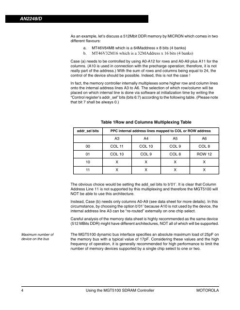
Table 1Row and Columns Multiplexing Table<br />
addr_sel bits PPC internal address lines mapped to COL or ROW address<br />
A3 A4 A5 A6<br />
00 COL 11 COL 10 COL 9 COL 8<br />
01 COL 10 COL 9 COL 8 ROW 12<br />
10 X X X X<br />
11 X X X X<br />
The obvious choice would be setting the add_sel bits to b’01’. It is clear that Column<br />
Address Line 11 is not supported by this multiplexing and therefore the MGT5100 will<br />
NOT be able to use this architecture.<br />
Instead, Case (b) needs only columns A0-A9 (see data sheet for more details). In this<br />
circumstance, by choosing the option b’01’ because A10 is not used by the device, the<br />
internal address line A3 can be “re-routed” externally on one chip select.<br />
Careful analysis of the memory data sheet is highly recommended as the same device<br />
(512 MBits DDR) might have different architectures, NOT all of which will be supported.<br />
The MGT5100 dynamic bus interface specifies an absolute maximum load of 25pF on<br />
the memory bus with a typical value of 17pF. Considering these values and the high<br />
frequency of operation, it is generally recommended for high performance to limit the<br />
number of memory devices supported by a single chip select to one or two.<br />
4 Using the MGT5100 SDRAM Controller MOTOROLA


