Design for Testability (II)
Design for Testability (II)
Design for Testability (II)

You also want an ePaper? Increase the reach of your titles
YUMPU automatically turns print PDFs into web optimized ePapers that Google loves.
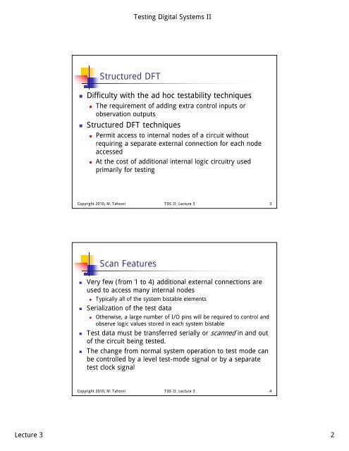
Structured DFT<br />
Testing Digital Systems <strong>II</strong><br />
Difficulty with the ad hoc testability techniques<br />
The requirement of adding extra control inputs or<br />
observation outputs<br />
Structured DFT techniques<br />
Permit access to internal nodes of a circuit without<br />
requiring a separate external connection <strong>for</strong> each node<br />
accessed<br />
At the cost of additional internal logic circuitry used<br />
primarily <strong>for</strong> testing<br />
Copyright 2010, M. Tahoori TDS <strong>II</strong>: Lecture 3 3<br />
Scan Features<br />
Very few (from 1 to 4) additional external connections are<br />
used to access many internal nodes<br />
Typically all of the system bistable elements<br />
Serialization of the test data<br />
Otherwise, a large number of I/O pins will be required to control and<br />
observe logic values stored in each system bistable<br />
Test data must be transferred serially or scanned in and out<br />
of the circuit being tested.<br />
The change from normal system operation to test mode can<br />
be controlled by a level test-mode signal or by a separate<br />
test clock signal<br />
Copyright 2010, M. Tahoori TDS <strong>II</strong>: Lecture 3 4<br />
Lecture 3 2