ANALOG INTEGRATED CIRCUITS DESIGN BY MEANS OF GENETIC ALGORITHMS ...
ANALOG INTEGRATED CIRCUITS DESIGN BY MEANS OF GENETIC ALGORITHMS ...
ANALOG INTEGRATED CIRCUITS DESIGN BY MEANS OF GENETIC ALGORITHMS ...

You also want an ePaper? Increase the reach of your titles
YUMPU automatically turns print PDFs into web optimized ePapers that Google loves.
evaluated, allowing a ranking of the best solutions found by<br />
GA.<br />
There are several works applying GA for EH related to<br />
analog circuits design [2-5]. For instance, the work presented in<br />
[3] shows GA for complex filters design, such as asymmetric<br />
filters, using frequency response analysis to evaluate the circuit.<br />
In [2], the authors present a solution to circuits design based on<br />
an external programmable analog multiplexer array (PAMA). In<br />
this work, each individual is a binary string, representing<br />
selection bits for multiplexer and demultiplexer, responsible for<br />
the PAMA interconnections. A D/A (digital to analog)<br />
converter board is used in PC to generate input signals to the<br />
circuit and an A/D (analog to digital) board is applied to collect<br />
output response. Based upon the response obtained for each<br />
individual, that represents a different solution, an evaluation is<br />
generated, ranking these solutions. In [4], a similar work to<br />
ours is presented where the authors apply GA in an Operational<br />
Transconductance Amplifier (OTA) design, but with different<br />
evaluation function and schematic.<br />
3. OUR GA SOLUTION FOR OTA OPTIMIZATION<br />
Our aim is to apply GA to design a SOI CMOS OTA, where<br />
the transistors dimensions are determined focusing on achieving<br />
the smallest OTA die area possible, defining automatically the<br />
values of transistors W and L of an OTA as shown in Fig. 1.<br />
The following sections describe our GA method to accomplish<br />
this task.<br />
3.1. Input data<br />
As the GA algorithm is based on the methodology that uses<br />
the curve of g m/I DS as a function of I DS/(W/L) [7], first of all, it<br />
is necessary to define the following information: dissipation<br />
power (P), supply voltage (V dd), channel width and length range<br />
of transistors (mainly minimum channel length value), Early<br />
voltage behavior as a function of channel length (V EAxL) and<br />
the g m/I DS x I DS/(W/L) curve of the technology to be used. When<br />
this information has been given, a reduction in the GA searches<br />
space occurs, eliminating unpractical solutions. The next step<br />
should be defined, in this study, the values of open-loop voltage<br />
gain and unit voltage gain frequency that the OTA has to<br />
operate. Additionally, the GA tool for analog IC design allows<br />
in this case, to define the number of rounds, crossover ratio,<br />
mutation ratio, number of individuals or potential solutions<br />
developed per generation and total generated individuals are<br />
adjustable as desired.<br />
3.2. Representation, evolution and evaluation<br />
Each individual in GA, meaning a potential solution, is<br />
represented as shown on Fig. 2, where W x and L x (x ∈ {4,6,8}),<br />
are the channel width and length of transistors that compose the<br />
OTA, respectively.<br />
Fig 2. Chromosome representation.<br />
Both W and L alleles in chromosome contain transistors<br />
dimensions (M4, M6, M8 or M3, M5, M7), represented in<br />
binary format containing each allele 11 bits and allowing<br />
reproduction by means of binary one-point crossover (where<br />
two solutions are split in two parts and have its contents<br />
swapped between them). For the case of M8, only L dimension<br />
is represented since the GA evaluation expression in this work<br />
doesn’t involve W 8 in the expression.<br />
The g m/I DS portion is an integer number that expresses the<br />
value of transconductance over current drain ratio for the<br />
differential input pair, represented by M1 and M2 transistors as<br />
shown on Fig. 1. The reason for the g m/I DS appears in the<br />
chromosome is due to the evaluation expression carried out<br />
during the GA process. For g m/I DS, the reproduction is<br />
performed using mean operation between two g m/I DS<br />
individuals.<br />
As the open loop gain (A V0) is the objective to be reached<br />
and we are not proposing a multiple-objective solution, the unit<br />
voltage gain frequency (f T) is simply monitored here.<br />
Performing GA software, each individual is evaluated, using<br />
evaluation expression of the open-loop voltage gain, described<br />
earlier in the equation (1). If A V0 is smaller than the desired<br />
open-loop voltage gain, the chromosome receives a lower<br />
evaluation than those chromosomes that present a solution<br />
closer to the desired open-loop voltage gain. Likewise,<br />
solutions with gains higher than the desired open-loop voltage<br />
gain should have lower evaluations. In this case, we have a<br />
symmetric problem, since the gain may assume values from<br />
minus infinite (-∞) up to plus infinite (+∞), and an intermediate<br />
value between is the interested region. Therefore, an impulse<br />
function (centered in the objective open-loop voltage gain<br />
value) to obtain the evaluation is not suitable in this case, once<br />
solutions with less or high open-loop voltage gain than the<br />
desired one may be useful for the reproduction process. The<br />
total part of these solutions will not met the objectives but if<br />
combined by means of reproduction with other solutions may<br />
result in solutions better than the best ones currently available.<br />
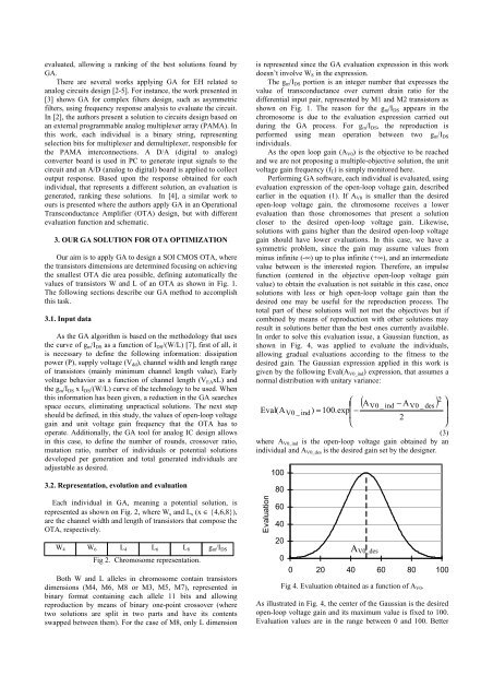
In order to solve this evaluation issue, a Gaussian function, as<br />
shown in Fig. 4, was applied to evaluate the individuals,<br />
allowing gradual evaluations according to the fitness to the<br />
desired gain. The Gaussian expression applied in this work is<br />
given by the following Eval(A V0_ind) expression, that assumes a<br />
normal distribution with unitary variance:<br />
2<br />
( A A ) ⎞<br />
V0<br />
_ ind V0<br />
_ des ⎟<br />
⎟<br />
⎛<br />
Eval(<br />
A<br />
⎜<br />
V0<br />
_ ind ) = 100.<br />
exp −<br />
⎜<br />
⎝<br />
−<br />
2<br />
⎠<br />
(3)<br />
where AV0_ind is the open-loop voltage gain obtained by an<br />
individual and AV0_des is the desired gain set by the designer.<br />
W 4 W 6 L 4 L 6 L 8 g m/I DS AV0_des<br />
Evaluation o<br />
100<br />
80<br />
60<br />
40<br />
20<br />
0<br />
0 20 40 60 80 100<br />
Fig 4. Evaluation obtained as a function of A V0.<br />
As illustrated in Fig. 4, the center of the Gaussian is the desired<br />
open-loop voltage gain and its maximum value is fixed to 100.<br />
Evaluation values are in the range between 0 and 100. Better