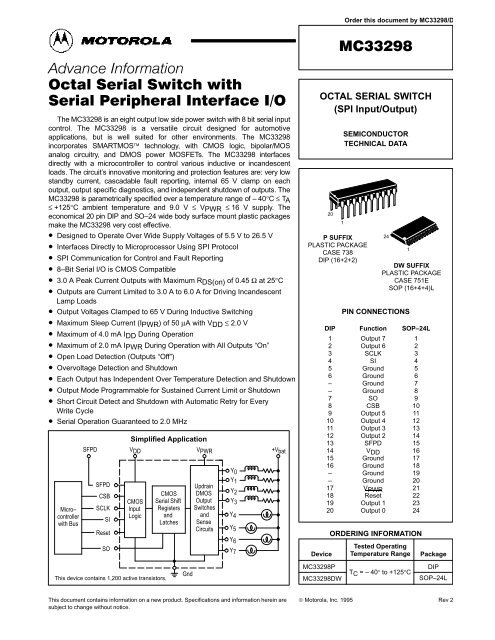
MC33298 Octal Serial Switch with Serial Peripheral Interface I/O
MC33298 Octal Serial Switch with Serial Peripheral Interface I/O
MC33298 Octal Serial Switch with Serial Peripheral Interface I/O

You also want an ePaper? Increase the reach of your titles
YUMPU automatically turns print PDFs into web optimized ePapers that Google loves.
The <strong>MC33298</strong> is an eight output low side power switch <strong>with</strong> 8 bit serial input<br />
control. The <strong>MC33298</strong> is a versatile circuit designed for automotive<br />
applications, but is well suited for other environments. The <strong>MC33298</strong><br />
incorporates SMARTMOS technology, <strong>with</strong> CMOS logic, bipolar/MOS<br />
analog circuitry, and DMOS power MOSFETs. The <strong>MC33298</strong> interfaces<br />
directly <strong>with</strong> a microcontroller to control various inductive or incandescent<br />
loads. The circuit’s innovative monitoring and protection features are: very low<br />
standby current, cascadable fault reporting, internal 65 V clamp on each<br />
output, output specific diagnostics, and independent shutdown of outputs. The<br />
<strong>MC33298</strong> is parametrically specified over a temperature range of – 40°C ≤ TA<br />
≤ +125°C ambient temperature and 9.0 V ≤ VPWR ≤ 16 V supply. The<br />
economical 20 pin DIP and SO–24 wide body surface mount plastic packages<br />
make the <strong>MC33298</strong> very cost effective.<br />
• Designed to Operate Over Wide Supply Voltages of 5.5 V to 26.5 V<br />
• <strong>Interface</strong>s Directly to Microprocessor Using SPI Protocol<br />
• SPI Communication for Control and Fault Reporting<br />
• 8–Bit <strong>Serial</strong> I/O is CMOS Compatible<br />
• 3.0 A Peak Current Outputs <strong>with</strong> Maximum RDS(on) of 0.45 Ω at 25°C<br />
• Outputs are Current Limited to 3.0 A to 6.0 A for Driving Incandescent<br />
Lamp Loads<br />
• Output Voltages Clamped to 65 V During Inductive <strong>Switch</strong>ing<br />
• Maximum Sleep Current (IPWR) of 50 μA <strong>with</strong> VDD ≤ 2.0 V<br />
• Maximum of 4.0 mA IDD During Operation<br />
• Maximum of 2.0 mA IPWR During Operation <strong>with</strong> All Outputs “On”<br />
• Open Load Detection (Outputs “Off”)<br />
• Overvoltage Detection and Shutdown<br />
• Each Output has Independent Over Temperature Detection and Shutdown<br />
• Output Mode Programmable for Sustained Current Limit or Shutdown<br />
• Short Circuit Detect and Shutdown <strong>with</strong> Automatic Retry for Every<br />
Write Cycle<br />
• <strong>Serial</strong> Operation Guaranteed to 2.0 MHz<br />
Micro–<br />
controller<br />
<strong>with</strong> Bus<br />
SFPD<br />
SFPD<br />
CSB<br />
SCLK<br />
SI<br />
Reset<br />
SO<br />
VDD<br />
CMOS<br />
Input<br />
Logic<br />
This device contains 1,200 active transistors.<br />
Simplified Application<br />
CMOS<br />
<strong>Serial</strong> Shift<br />
Registers<br />
and<br />
Latches<br />
MOTOROLA ANALOG IC DEVICE DATA<br />
VPWR<br />
Updrain<br />
DMOS<br />
Output<br />
<strong>Switch</strong>es<br />
and<br />
Sense<br />
Circuits<br />
+Vbat<br />
This document contains information on a new product. Specifications and information herein are<br />
subject to change <strong>with</strong>out notice.<br />
Gnd<br />
Y0<br />
Y1<br />
Y2<br />
Y3<br />
Y4<br />
Y5<br />
Y6<br />
Y7<br />
Device<br />
<strong>MC33298</strong>P<br />
<br />
OCTAL SERIAL SWITCH<br />
(SPI Input/Output)<br />
20<br />
P SUFFIX<br />
PLASTIC PACKAGE<br />
CASE 738<br />
DIP (16+2+2)<br />
<strong>MC33298</strong>DW<br />
1<br />
Order this document by <strong>MC33298</strong>/D<br />
SEMICONDUCTOR<br />
TECHNICAL DATA<br />
24<br />
PIN CONNECTIONS<br />
ORDERING INFORMATION<br />
Tested Operating<br />
Temperature Range Package<br />
TC = – 40° to +125°C<br />
1<br />
DW SUFFIX<br />
PLASTIC PACKAGE<br />
CASE 751E<br />
SOP (16+4+4)L<br />
DIP Function SOP–24L<br />
1<br />
2<br />
3<br />
4<br />
5<br />
6<br />
–<br />
–<br />
7<br />
8<br />
9<br />
10<br />
11<br />
12<br />
13<br />
14<br />
15<br />
16<br />
–<br />
–<br />
17<br />
18<br />
19<br />
20<br />
Output 7<br />
Output 6<br />
SCLK<br />
SI<br />
Ground<br />
Ground<br />
Ground<br />
Ground<br />
SO<br />
CSB<br />
Output 5<br />
Output 4<br />
Output 3<br />
Output 2<br />
SFPD<br />
VDD<br />
Ground<br />
Ground<br />
Ground<br />
Ground<br />
VPWR<br />
Reset<br />
Output 1<br />
Output 0<br />
1<br />
2<br />
3<br />
4<br />
5<br />
6<br />
7<br />
8<br />
9<br />
10<br />
11<br />
12<br />
13<br />
14<br />
15<br />
16<br />
17<br />
18<br />
19<br />
20<br />
21<br />
22<br />
23<br />
24<br />
DIP<br />
SOP–24L<br />
© Motorola, Inc. 1995 Rev 2<br />
1
VDD<br />
SFPD<br />
Reset<br />
CSB<br />
SCLK<br />
SI<br />
SO<br />
20 μA<br />
20 μA<br />
Fault<br />
Timers<br />
<strong>Serial</strong> D/O<br />
Line Driver<br />
Overvoltage<br />
Detect<br />
SERIAL OUTPUT (SO) PIN REPORTS<br />
OVD<br />
RB<br />
SFPDB<br />
SFL<br />
CSB<br />
SCLK<br />
SI<br />
SO<br />
CSI<br />
CSBI<br />
<strong>MC33298</strong><br />
Figure 1. Simplified Block Diagram<br />
SPI<br />
<strong>Interface</strong><br />
Logic<br />
VPWR<br />
Voltage<br />
Regulator<br />
GE<br />
OT<br />
SF<br />
OF<br />
Gate<br />
Control<br />
2 MOTOROLA ANALOG IC DEVICE DATA<br />
Bias<br />
FAULT OPERATION<br />
Overvoltage Overvoltage condition reported.<br />
Over Temperature Fault reported by <strong>Serial</strong> Output (SO) pin.<br />
Open<br />
Load<br />
Detect<br />
Short<br />
Circuit<br />
Detect<br />
Over<br />
Temperature<br />
Detect<br />
From Detectors 1 to 7<br />
Over Current SO pin reports short to battery/supply or over current condition.<br />
Output “On,” Open Load Fault Not reported.<br />
Output “Off,” Open Load Fault SO pin reports output “off” open load condition.<br />
DEVICE SHUTDOWNS<br />
65 V<br />
ILimit<br />
To Gates<br />
1 – 7<br />
Overvoltage Total device shutdown at VPWR = 28–36 V. Re–operates when overvoltage is removed <strong>with</strong><br />
all outputs assuming an off state upon recovery from overvoltage. All device registers are<br />
automatically reset (cleared) during shutdown.<br />
Over Temperature Only the output experiencing an over temperature shuts down.<br />
Over Current Only the output experiencing an over current condition shuts down at 3.0 A to 6.0 A after a<br />
25 μs to 100 μs delay, <strong>with</strong> SFPD pin grounded. All outputs will continue to operate in a current<br />
limit mode, <strong>with</strong> no shutdown, if the SPFD pin is at 5.0 V.<br />
RS<br />
Output 0<br />
Outputs<br />
1 – 7<br />
Grounds
<strong>MC33298</strong><br />
MAXIMUM RATINGS (All voltages are <strong>with</strong> respect to ground, unless otherwise noted.)<br />
MOTOROLA ANALOG IC DEVICE DATA<br />
Rating Symbol Value Unit<br />
Power Supply Voltage<br />
Steady–State VPWR(sus) –1.5 to 26.5 V<br />
Transient Conditions (Note1) VPWR(pk) –13 to 60 V<br />
Logic Supply Voltage (Note 2) VDD – 0.3 to 7.0 V<br />
Input Pin Voltage (Note 3) VIN – 0.3 to 7.0 V<br />
Output Clamp Voltage (Note 4) VOUT(off) V<br />
(2.0 mA ≤ Iout ≤ 0.5 A) 50 to 75<br />
Output Self–Limit Current IOUT(lim) 3.0 to 6.0 A<br />
Continuous Per Output Current (Note 5) IOUT(cont) 1.0 A<br />
ESD Voltage<br />
Human Body Model (Note 6) VESD1 2000 V<br />
Machine Model (Note 7) VESD2 200 V<br />
Output Clamp Energy (Note 8) Eclamp<br />
Repetitive:<br />
TJ = 25°C 100 mJ<br />
TJ = 125°C 30 mJ<br />
Non–Repetitive:<br />
TJ = 25°C 2.0 J<br />
TJ = 125°C 0.5 J<br />
Recommended Frequency of SPI Operation (Note 9) fSPI 2.0 MHz<br />
Storage Temperature Tstg – 55 to +150 °C<br />
Operating Case Temperature TC – 40 to +125 °C<br />
Operating Junction Temperature TJ – 40 to +150 °C<br />
Power Dissipation (TA = 25°C) (Note 10) PD 3.0 W<br />
Soldering Temperature (for 10 seconds) Tsolder 260 °C<br />
Thermal Resistance, Junction–to–Ambient (Note 11) RθJA °C/W<br />
Plastic Package, Case 738:<br />
All Outputs “On” (Note 12) 31<br />
Single Output “On” (Note 13) 37<br />
SOP–24 Package, Case 751E:<br />
All Outputs “On” (Note 12) 34<br />
Single Output (Note 13) 40<br />
NOTES: 1. Transient capability <strong>with</strong> external 100 Ω resistor connected in series <strong>with</strong> V PWR pin and supply.<br />
2. Exceeding these limits may cause a malfunction or permanent damage to the device.<br />
3. Exceeding voltage limits on SCLK, SI, CSB, SFPD, or Reset pins may cause permanent damage to<br />
the device.<br />
4. With output “off.”<br />
5. Continuous output rating so long as maximum junction temperature is not exceeded. (See Figure 21 and<br />
22 for more details).<br />
6. ESD1 testing is performed in accordance <strong>with</strong> the Human Body Model (C Zap = 100 pF, R Zap = 1500 Ω).<br />
7. ESD2 testing is performed in accordance <strong>with</strong> the Machine Model (C Zap = 100 pF, R Zap = 0 Ω).<br />
8. Maximum output clamp energy capability at indicated Junction Temperature using single pulse method.<br />
See Figure 19 for more details.<br />
9. Guaranteed and production tested for 2.0 MHz SPI operation but has been demonstrated to operate to<br />
8.5 MHz @ 25°C.<br />
10. Maximum power dissipation at indicated junction temperature <strong>with</strong> no heat sink used. See Figures 20,<br />
21, and 22 for more details.<br />
11. See Figure 20 for Thermal Model.<br />
12. Thermal resistance from Junction–to–Ambient <strong>with</strong> all outputs “on” and dissipating equal power.<br />
13. Thermal resistance from Junction–to–Ambient <strong>with</strong> a single output “on.”<br />
3
<strong>MC33298</strong><br />
STATIC ELECTRICAL CHARACTERISTICS (Characteristics noted under conditions of 4.5 V ≤ VDD ≤ 5.5 V, 9.0 V ≤VPWR ≤ 16 V,<br />
– 40°C ≤ TC ≤ 125°C, unless otherwise noted.)<br />
POWER INPUT<br />
Characteristic Symbol Min Typ Max Unit<br />
Supply Voltage Range V<br />
Quasi–Functional (Note 1) VPWR(qf) 5.5 – 9.0<br />
Full Operational VPWR(fo) 9.0 – 26.5<br />
Supply Current (all Outputs “On,” Iout = 0.5 A) (Note 2) IPWR(on) – 1.0 2.0 mA<br />
Sleep State Supply Current (VDD = 0.5 V) IPWR(ss) – 1.0 50 μA<br />
Sleep State Output Leakage Current (per Output, VDD = 0.5 V) IOUT(ss) – – 50 μA<br />
Overvoltage Shutdown VOV 28 – 36 V<br />
Overvoltage Shutdown Hysteresis VOV(hys) 0.2 – 1.5 V<br />
Logic Supply Voltage VDD 4.5 – 5.5 V<br />
Logic Supply Current (<strong>with</strong> any combination of Outputs “On”) IDD – – 4.0 mA<br />
Logic Supply Undervoltage Lockout Threshold (Note 3) VDD(uvlo) 2.0 – 4.5 V<br />
POWER OUTPUT<br />
Drain–to–Source “On” Resistance (Iout = 0.5 A, TJ = 25°C) RDS(on) Ω<br />
VPWR = 5.5 V – – 1.0<br />
VPWR = 9.0 V – 0.4 0.5<br />
VPWR = 13 V – 0.35 0.45<br />
Drain–to–Source “On” Resistance (Iout = 0.5 A, TJ = 150°C) RDS(on) Ω<br />
VPWR = 5.5 V – – 1.8<br />
VPWR = 9.0 V – 0.75 0.9<br />
VPWR = 13 V – 0.65 0.8<br />
Output Self–Limiting Current IOUT(lim) A<br />
Outputs Programmed “On”, Vout = 0.6 VDD 3.0 4.0 6.0<br />
Output Fault Detect Threshold (Note 4) VOUTth(F) VDD<br />
Output Programmed “Off” 0.6 0.7 0.8<br />
Output “Off” Open Load Detect Current (Note 5) IOCO μA<br />
Output Programmed “Off,” Vout = 0.6 VDD 30 50 100<br />
Output Clamp Voltage VOK V<br />
2.0 mA≤ Iout ≤ 200 mA 50 60 75<br />
Output Leakage Current (VDD ≤ 2.0 V) (Note 6) IOUT(lkg) – 50 0 50 μA<br />
Over Temperature Shutdown (Outputs “Off”) (Note 7) TLIM 155 170 185 °C<br />
Over Temperature Shutdown Hysteresis (Note 7) TLIM(hys) – 10 20 °C<br />
NOTES: 1. SPI inputs and outputs operational; Fault reporting may not be fully operational <strong>with</strong>in this voltage range.<br />
2. Value reflects normal operation (no faults) <strong>with</strong> all outputs “on.” Each “on” output contributes approximately 20 μA to I PWR . Each output experiencing<br />
a “soft short” condition contributes approximately 0.5 mA to I PWR . A “soft short” is defined as any load current causing the output source current to<br />
self–limit. A “hard” output short is a very low impedance short to supply.<br />
3. For V DD less than the Undervoltage Lockout Threshold voltage, all data registers are reset and all outputs are disabled.<br />
4. Output fault detect threshold <strong>with</strong> outputs programmed “off.” Output fault detect thresholds are the same for output opens and shorts.<br />
5. Output “Off” Open Load Detect Current is the current required to flow through the load for the purpose of detecting the existence of an open condition<br />
when the specific output is commanded to be “off.”<br />
6. Output leakage current measured <strong>with</strong> output “off” and at 16 V.<br />
7. This parameter is guaranteed by design but is not production tested.<br />
4 MOTOROLA ANALOG IC DEVICE DATA
<strong>MC33298</strong><br />
STATIC ELECTRICAL CHARACTERISTICS (Characteristics noted under conditions of 4.5 V ≤ VDD ≤ 5.5 V, 9.0 V ≤VPWR ≤ 16 V,<br />
– 40°C ≤ TC ≤ 125°C, unless otherwise noted.)<br />
DIGITAL INTERFACE<br />
MOTOROLA ANALOG IC DEVICE DATA<br />
Characteristic Symbol Min Typ Max Unit<br />
Input Logic High Voltage (Note 1) VIH 0.7 – 1.0 VDD<br />
Input Logic Low Voltage (Note 2) VIL 0.0 – 0.2 VDD<br />
Input Logic Voltage Hysteresis (Note 3) VI(hys) 50 100 500 mV<br />
Input Logic Current (Note 4) IIN –10 0 10 μA<br />
Reset Pull–Up Current (Reset = 0.7 VDD) IRSTB 10 22 50 μA<br />
SFPD Pull–Down Current (SFPD = 0.2 VDD) ISFPD 10 22 50 μA<br />
SO High State Output Voltage (IOH = 1.0 mA) VSOH VDD –1.0 V VDD – 0.6 V – V<br />
SO Low State Output Voltage (IOL = –1.6 mA) VSOL – 0.2 0.4 V<br />
SO Tri–State Leakage Current (CSB = 0.7 VDD, 0 V ≤ VSO ≤ VDD) ISOT – 10 0 10 μA<br />
Input Capacitance (0 V ≤ VDD ≤ 5.5 V) (Note 5) CIN – – 12 pF<br />
SO Tri–State Capacitance (0 V ≤ VDD ≤ 5.5 V) (Note 6) CSOT – – 20 pF<br />
NOTES: 1. Upper logic threshold voltage range applies to SI, CSB, SCLK, Reset, and SFPD input signals.<br />
2. Lower logic threshold voltage range applies to SI, CSB, SCLK, Reset, and SFPD input signals.<br />
3. Only the SFPD and Reset inputs have hysteresis. This parameter is guaranteed by design but is not production tested.<br />
4. Input current of SCLK, SI, and CSB logic control inputs.<br />
5. Input capacitance of SI, CSB, SCLK, Reset, and SFPD for 0 V ≤ V DD ≤ 5.5 V. This parameter is guaranteed by design, but is not production tested.<br />
6. Tri–state capacitance of SO for 0 V ≤ V DD ≤ 5.5 V. This parameter is guaranteed by design but is not production tested.<br />
RSTB<br />
CSB<br />
SCLK<br />
SI<br />
0.2 VDD<br />
twRSTB<br />
Don’t Care<br />
0.2 VDD<br />
0.7 VDD<br />
Figure 2. Input Timing <strong>Switch</strong> Characteristics<br />
tlead<br />
tSISU<br />
0.7 VDD<br />
0.2 VDD<br />
twSCLKH<br />
0.2 VDD<br />
Valid<br />
twSCLKL<br />
tSI(hold)<br />
tr<br />
tf<br />
tlag<br />
Don’t Care Valid<br />
Don’t Care<br />
VIH<br />
VIL<br />
VIH<br />
VIL<br />
VIH<br />
VIL<br />
VIH<br />
VIL<br />
5
<strong>MC33298</strong><br />
DYNAMIC ELECTRICAL CHARACTERISTICS (Characteristics noted under conditions of 4.5 V ≤ VDD ≤ 5.5 V,<br />
9.0 V ≤ VPWR ≤ 16 V, – 40°C ≤ TC ≤ 125°C, unless otherwise noted.)<br />
POWER OUTPUT TIMING<br />
Characteristic Symbol Min Typ Max Unit<br />
Output Rise Time (VPWR = 13 V, RL = 26 Ω) (Note 1) tr 0.4 1.5 20 μs<br />
Output Fall Time (VPWR = 13 V, RL = 26 Ω) (Note 1) tf 0.4 2.5 20 μs<br />
Output Turn “On” Delay Time (VPWR = 13 V, RL = 26 Ω) (Note 2) tdly(on) 1.0 5.0 15 μs<br />
Output Turn “Off” Delay Time (VPWR = 13 V, RL = 26 Ω) (Note 3) tdly(off) 1.0 5.0 15 μs<br />
Output Short Fault Disable Report Delay (Note 4) tdly(sf) μs<br />
SFPD = 0.2 x VDD 25 50 100<br />
Output “Off” Fault Report Delay (Note 5) tdly(off) μs<br />
SFPD = 0.2 x VDD 25 50 100<br />
NOTES: 1. Output Rise and Fall time respectively measured across a 26 Ω resistive load at 10% to 90% and 90% to 10% voltage points.<br />
2. Output Turn “On” Delay time measured from rising edge of CSB to 50% of output “off” V out voltage <strong>with</strong> R L = 26 Ω resistive load<br />
(see Figure 7 and 8).<br />
3. Output Turn “Off” Delay time measured from rising edge of CSB to 50% of output “off” V out voltage <strong>with</strong> R L = 26 Ω resistive load<br />
(see Figure 7 and 8).<br />
4. Output Short Fault Disable Report Delay measured from rising edge of CSB to I out = 2.0 A point <strong>with</strong> output “on,” V out = 5.0 V,<br />
and SFPD = 0.2 x V DD (see Figure 9 and 10).<br />
5. Output “Off” Fault Report Delay measured from 50% points of rising edge of CSB to rising edge of output (see Figure 8).<br />
DYNAMIC ELECTRICAL CHARACTERISTICS (Characteristics noted under conditions of 4.5 V ≤ VDD ≤ 5.5 V,<br />
9.0 V ≤VPWR ≤ 16 V, – 40°C ≤ TC ≤ 125°C, unless otherwise noted.)<br />
DIGITAL INTERFACE TIMING<br />
Characteristic Symbol Min Typ Max Unit<br />
SCLK Clock Period (Note 6) tpSCLK 500 – – ns<br />
SCLK Clock High Time twSCLKH 175 – – ns<br />
SCLK Clock Low Time twSCLKL 175 – – ns<br />
Required Low State Duration for Reset (VIL ≤ 0.2 VDD) (Note 1) twRSTB 250 50 – ns<br />
Falling Edge of CSB to Rising Edge of SCLK (Required Setup Time) tlead 250 50 – ns<br />
Falling Edge of SCLK to Rising Edge of CSB (Required Setup Time) tlag 250 50 – ns<br />
SI to Falling Edge of SCLK (Required Setup Time) tSISU 125 25 – ns<br />
Falling Edge of SCLK to SI (Required Hold Time) tSI(hold) 125 25 – ns<br />
SO Rise Time (CL = 200 pF) trSO – 25 75 ns<br />
SO Fall Time (CL = 200 pF) tfSO – 25 75 ns<br />
SI, CSB, SCLK Incoming Signal Rise Time (Note 2) trSI – – 200 ns<br />
SI, CSB, SCLK Incoming Signal Fall TIme (Note 2) tfSI – – 200 ns<br />
Time from Falling Edge of CSB to SO ns<br />
Low Impedance (Note 3) tSO(en) – – 200<br />
HIgh Impedance (Note 4) tSO(dis) – – 200<br />
Time from Rising Edge of SCLK to SO Data Valid (Note 5) tvalid<br />
0.2 VDD ≤ SO ≥ 0.8 VDD, CL = 200 pF – 50 125 ns<br />
NOTES: 1. Reset Low duration measured <strong>with</strong> outputs enabled and going to “off” or disabled condition.<br />
2. Rise and Fall time of incoming SI, CSB, and SCLK signals suggested for design consideration to prevent the occurrence of double pulsing.<br />
3. Time required for output status data to be available for use at SO.<br />
4. Time required for output status data to be terminated at SO.<br />
5. Time required to obtain valid data out from SO following the rise of SCLK.<br />
6. Clock period includes 75 ns rise plus 75 ns fall transition time in addition to clock high and low time.<br />
6 MOTOROLA ANALOG IC DEVICE DATA
SCLK<br />
SO<br />
(Low–to–High)<br />
SO<br />
SCLK<br />
Figure 3. Valid Data Delay Time and<br />
Valid Time Test Circuit<br />
VDD = 5.0 V<br />
<strong>MC33298</strong><br />
Under<br />
Test<br />
MOTOROLA ANALOG IC DEVICE DATA<br />
SO<br />
CL = 200 pF<br />
C L represents the total capacitance of the test fixture and probe.<br />
(High–to–Low)<br />
Figure 4. Vaild Data Delay Time and<br />
Valid Time Waveforms<br />
trSI<br />
0.7 VDD (2.5 V)<br />
tdly(lh)<br />
0.2 VDD<br />
tvalid<br />
0.7 VDD<br />
tdly(hl)<br />
≤ 10 ns<br />
50%<br />
trSO<br />
tfSO<br />
0.7 VDD<br />
0.2 VDD<br />
tfSI<br />
≤ 10 ns<br />
0.2 VDD<br />
SO (low–to–high) is for an output <strong>with</strong> internal conditions such that<br />
the low–to–high transition of CSB causes the SO output to switch<br />
from high–to–low.<br />
<strong>MC33298</strong><br />
5.0 V<br />
0<br />
VOH<br />
VOL<br />
VOH<br />
VOL<br />
CSB<br />
SO<br />
SO<br />
Figure 5. Enable and Disable Time Test Circuit<br />
CSB<br />
VDD = 5.0 V<br />
<strong>MC33298</strong><br />
Under<br />
Test<br />
VPull–Up = 2.5 V<br />
RL = 2.0 kΩ<br />
SO<br />
CL = 20 pF<br />
C L represents the total capacitance of the test fixture and probe.<br />
Figure 6. Enable and Disable Time Waveforms<br />
(High–to–Low)<br />
0.7 VDD<br />
0.2 VDD (2.5 V)<br />
(Low–to–High)<br />
trSI<br />
≤ 10 ns<br />
tSO(en)<br />
tSO(en)<br />
90%<br />
50%<br />
10%<br />
50%<br />
50%<br />
tfSI<br />
≤ 10 ns<br />
tSO(dis)<br />
tSO(dis)<br />
NOTES: 1. SO (high–to–low) waveform is for SO output <strong>with</strong> internal<br />
conditions such that SO output is low except when an output is<br />
disabled as a result of detecting a circuit fault <strong>with</strong> CSB in a<br />
High Logic state (e.g., open load).<br />
2. SO (low–to–high) waveform is for SO output <strong>with</strong> internal<br />
conditions such that SO output is high except when an output<br />
is disabled as a result of detecting a circuit fault <strong>with</strong> CSB in<br />
a High Logic state (e.g., shorted load).<br />
5.0 V<br />
VOH<br />
VOL<br />
VOH<br />
VOL<br />
7<br />
0
CSB<br />
CSB<br />
Output Voltage<br />
Waveform 1<br />
Output Voltage<br />
Waveform 2<br />
Figure 7. <strong>Switch</strong>ing Time Test Circuit<br />
VDD = 5.0 V<br />
<strong>MC33298</strong><br />
Under<br />
Test<br />
VPWR = 14 V<br />
RL = 26 Ω<br />
CL<br />
Output<br />
C L represents the total capacitance of the test fixture and probe.<br />
Figure 8. Turn–On/Off Waveforms<br />
10%<br />
trSI<br />
≤ 10 ns<br />
90%<br />
50%<br />
tdly(off)<br />
tdly(on)<br />
50%<br />
50%<br />
tfSI<br />
≤ 10 ns<br />
90%<br />
50% 10%<br />
NOTES: 1. t dly(on) and t dly(off) are turn–on and turn–off propagation<br />
delay times.<br />
2. Waveform 1 is an output programmed from an “on” to an<br />
“off” state.<br />
3. Waveform 2 is an output programmed from an “off” to an<br />
“on” state.<br />
<strong>MC33298</strong><br />
5.0 V<br />
0<br />
14 V<br />
VOL<br />
14 V<br />
VOL<br />
8 MOTOROLA ANALOG IC DEVICE DATA<br />
CSB<br />
CSB<br />
Output Voltage<br />
Waveform<br />
Output Current<br />
Waveform<br />
Figure 9. Output Fault Unlatch Disable<br />
Delay Test Circuit<br />
VDD = 5.0 V<br />
<strong>MC33298</strong><br />
Under<br />
Test<br />
VPWR = 11 V<br />
IL = 2.0 A<br />
(Output “On”)<br />
Output<br />
CL = 20 pF<br />
C L represents the total capacitance of the test fixture and probe.<br />
Figure 10. Output Fault Unlatch Disable<br />
Delay Waveforms<br />
10%<br />
trSI<br />
tfSI<br />
≤ 10 ns ≤ 10 ns<br />
90%<br />
50%<br />
tdly(off)<br />
50%<br />
50%<br />
90%<br />
10%<br />
Voff = 11 V<br />
IO(CL)<br />
5.0 V<br />
0<br />
Von = 5.0 V<br />
NOTES: 1. t pdly(off) is the output fault unlatch disable propagation delay<br />
time required to correctly report an output fault after CSB rises.<br />
Represents an output commanded “on” while having an existing<br />
output short (overcurrent) to supply.<br />
2. SFPD pin ≤ 0.2 V.<br />
0
Introduction<br />
The <strong>MC33298</strong> was conceived, specified, designed, and<br />
developed for automotive applications. It is an eight output<br />
low side power switch having 8–bit serial control. The<br />
<strong>MC33298</strong> incorporates SMARTMOS technology having<br />
effective 2.0 μ CMOS logic, bipolar/MOS analog circuitry, and<br />
independent state of the art double diffused MOS (DMOS)<br />
power output transistors. Many benefits are realized as a<br />
direct result of using this mixed technology. A simplified block<br />
diagram of the <strong>MC33298</strong> is shown in Figure 1.<br />
Where bipolar devices require considerable control<br />
current for their operation, structured MOS devices, since<br />
they are voltage controlled, require only transient gate<br />
charging current affording a significant decrease in power<br />
consumption. The CMOS capability of the SMARTMOS<br />
process allows significant amounts of logic to be<br />
economically incorporated into the monolithic design. In<br />
addition, bipolar/MOS analog circuits embedded <strong>with</strong>in the<br />
updrain power DMOS output transistors monitor and provide<br />
fast, independent protection control functions for each<br />
individual output. All outputs have internal 65 V at 0.5 A<br />
independent output voltage clamps to provide fast inductive<br />
turn–off and transient protection.<br />
The <strong>MC33298</strong> uses high efficiency updrain power DMOS<br />
output transistors exhibiting very low drain to source “on”<br />
resistance values (RDS(on) ≤ 0.45 Ω) and dense CMOS<br />
control logic. Operational bias currents of less than 4.0 mA<br />
(1.0 mA typical) <strong>with</strong> any combination of outputs “on” are the<br />
result of using this mixed technology and would not be<br />
possible <strong>with</strong> bipolar structures. To accomplish a comparable<br />
functional feature set using a bipolar structure approach<br />
would result in a device requiring hundreds of milliamperes of<br />
internal bias and control current. This would represent a very<br />
large amount of power to be consumed by the device itself<br />
and not available for load use.<br />
In operation the <strong>MC33298</strong> functions as an eight output<br />
serial switch serving as a microcontroller (MCU) bus<br />
expander and buffer <strong>with</strong> fault management and fault<br />
reporting features. In doing so, the device directly relieves<br />
the MCU of the fault management functions. The <strong>MC33298</strong><br />
directly interfaces to an MCU and operates at system clock<br />
serial frequencies in excess of 2.0 MHz using a Synchronous<br />
<strong>Peripheral</strong> <strong>Interface</strong> (SPI) for control and diagnostic readout.<br />
MC68XX<br />
Microcontroller<br />
SPI<br />
SCLK<br />
Parallel Port<br />
MISO<br />
IRQ<br />
MOSI<br />
CSB SCLK<br />
SO SI<br />
<strong>MC33298</strong><br />
8 Outputs<br />
MOTOROLA ANALOG IC DEVICE DATA<br />
<strong>MC33298</strong><br />
CIRCUIT DESCRIPTION<br />
CSB SCLK<br />
SO SI<br />
<strong>MC33298</strong><br />
8 Outputs<br />
Figure 11 shows the basic SPI configuration between an<br />
MCU and one <strong>MC33298</strong>.<br />
Figure 11. SPI <strong>Interface</strong> <strong>with</strong> Microcontroller<br />
MC68HCXX<br />
Microcontroller<br />
Shift Register<br />
Receive<br />
Buffer<br />
Parallel<br />
Ports<br />
MOSI<br />
MISO<br />
SCLK<br />
Reset<br />
CSB<br />
SI<br />
SO<br />
<strong>MC33298</strong><br />
Shift Register<br />
To<br />
Logic<br />
The circuit can also be used in a variety of other<br />
applications in the computer, telecommunications, and<br />
industrial fields. It is parametrically specified over an input<br />
“battery”/supply range of 9.0 V to 16 V but is designed to<br />
operate over a considerably wider range of 5.5 V to 26.5 V.<br />
The design incorporates the use of Logic Level MOSFETs as<br />
output devices. These MOSFETs are sufficiently turned “on”<br />
<strong>with</strong> a gate voltage of less than 5.0 V thus eliminating the<br />
need for an internal charge pump. Each output is identically<br />
sized and independent in operation. The efficiency of each<br />
output transistor is such that <strong>with</strong> as little as 9.0 V supply<br />
(VPWR), the maximum RDS(on) of an output at room<br />
temperature is 0.45 Ω (0.35 Ω typical) and increases to only<br />
1.0 Ω (0.5 Ω typical) as VPWR is decreased to 5.5 V.<br />
All inputs are compatible <strong>with</strong> 5.0 V CMOS logic levels and<br />
incorporate negative or inverted logic. Whenever an input is<br />
programmed to a logic low state (< 1.0 V) the corresponding<br />
low side switched output being controlled will be active low<br />
and turned “on.” Conversely, whenever an input is<br />
programmed to a logic high state (> 3.0 V), the output being<br />
controlled will be high and turned “off.”<br />
Figure 12. <strong>MC33298</strong> SPI System Daisy Chain<br />
CSB SCLK<br />
SO SI<br />
<strong>MC33298</strong><br />
8 Outputs<br />
CSB SCLK<br />
SO SI<br />
<strong>MC33298</strong><br />
8 Outputs<br />
9
One main advantage of the <strong>MC33298</strong> is the serial port<br />
which when coupled to an MCU, receives “on”/“off”<br />
commands from the MCU and in return transmits the drain<br />
status of the device’s output switches. Many devices can be<br />
“daisy–chained” together to form a larger system (see<br />
Figure 12). Note in this example that only one dedicated<br />
MCU parallel port (aside from the required SPI) is needed for<br />
chip select to control 32 possible loads.<br />
Multiple <strong>MC33298</strong> devices can also be controlled in a<br />
parallel input fashion using SPI (see Figure 13). This figure<br />
shows a possible 24 loads being controlled by only three<br />
dedicated parallel MCU ports used for chip select.<br />
MC68XX<br />
CSB<br />
Microconttoller<br />
SPI <strong>MC33298</strong><br />
SI<br />
Parallel<br />
Ports<br />
Figure 13. Parallel Input SPI Control<br />
A0<br />
A1<br />
A2<br />
MOSI<br />
SCLK<br />
SI<br />
SCLK<br />
SCLK<br />
CSB<br />
SI<br />
SCLK<br />
CSB<br />
<strong>MC33298</strong><br />
<strong>MC33298</strong><br />
<strong>MC33298</strong><br />
8 Outputs<br />
8 Outputs<br />
8 Outputs<br />
Figure 14 shows a basic method of controlling multiple<br />
<strong>MC33298</strong> devices using two MCUs. A system can have only<br />
one master MCU at any given instant of time and one or more<br />
slave MCUs. The master MCU supplies the system clock<br />
signal (top MCU designated the master); the lower MCU<br />
being the slave. It is possible to have a system <strong>with</strong> more<br />
than one master but not at the same time. Only when the<br />
master is not communicating can a slave communicate. MCU<br />
master control is switched through the use of the slave select<br />
(SS) pin of the MCUs. A master will become a slave when it<br />
detects a logic low state on its SS pin.<br />
These basic examples make the <strong>MC33298</strong> very attractive<br />
for applications where a large number of loads need be<br />
controlled efficiently. The popular Synchronous <strong>Serial</strong><br />
<strong>Peripheral</strong> <strong>Interface</strong> (SPI) protocol is incorporated, to this<br />
end, to communicate efficiently <strong>with</strong> the MCU.<br />
SPI System Attributes<br />
The SPI system is flexible enough to communicate directly<br />
<strong>with</strong> numerous standard peripherals and MCUs available<br />
from Motorola and other semiconductor manufacturers. SPI<br />
reduces the number of pins necessary for input/output (I/O)<br />
on the <strong>MC33298</strong>. It also offers an easy means of expanding<br />
the I/O function using few MCU pins. The SPI system of<br />
communication consists of the MCU transmitting, and in<br />
return, receiving one databit of information per clock cycle.<br />
Databits of information are simultaneously transmitted by<br />
one pin, Microcontroller Out <strong>Serial</strong> In (MOSI), and received<br />
by another pin, Microcontroller In <strong>Serial</strong> Out (MISO), of<br />
the MCU.<br />
Some features of SPI are:<br />
• Full Duplex, Three–Wire Synchronous Data Transfer<br />
• Each Microcontroller can be a Master or a Slave<br />
• Provides Write Collision Flag Protection<br />
• Provides End of Message Interrupt Flag<br />
• Four I/Os associated <strong>with</strong> SPI (MOSI, MISO, SCLK, SS)<br />
The only drawbacks to SPI are that an MCU is required for<br />
efficient operational control and, in contrast to parallel input<br />
control, is slower at performing pulse width modulating<br />
(PWM) functions.<br />
<strong>MC33298</strong><br />
CSB<br />
SCLK<br />
8–Bit<br />
SO<br />
SI<br />
<strong>MC33298</strong><br />
CSB<br />
SCLK<br />
8–Bit<br />
SO<br />
<strong>MC33298</strong><br />
CSB<br />
SCLK<br />
8–Bit<br />
SO<br />
10 MOTOROLA ANALOG IC DEVICE DATA<br />
VDD<br />
VDD<br />
MC68XX<br />
Microcontroller<br />
SPI<br />
(Master)<br />
B0<br />
B1<br />
SS<br />
Figure 14. Multiple MCU SPI Control<br />
Parallel<br />
Ports<br />
8–Bit<br />
A0<br />
A1<br />
A2<br />
SCLK<br />
MISO<br />
MOSI<br />
MC68XX<br />
Microcontroller<br />
SPI<br />
(Alternate<br />
Master)<br />
B0<br />
B1<br />
SS<br />
Parallel<br />
Ports<br />
8–Bit<br />
A0<br />
A1<br />
A2<br />
SCLK<br />
MISO<br />
MOSI<br />
SI<br />
SI<br />
8 Outputs<br />
8 Outputs<br />
8 Outputs
CSB Pin<br />
The system MCU selects the <strong>MC33298</strong> to be<br />
communicated <strong>with</strong> through the use of the CSB pin.<br />
Whenever the pin is in a logic low state, data can be<br />
transferred from the MCU to the <strong>MC33298</strong> and vise versa.<br />
Clocked–in data from the MCU is transferred from the<br />
<strong>MC33298</strong> shift register and latched into the power outputs on<br />
the rising edge of the CSB signal. On the falling edge of the<br />
CSB signal, drain status information is transferred from the<br />
power outputs and loaded into the device’s shift register. The<br />
CSB pin also controls the output driver of the serial output<br />
pin. Whenever the CSB pin goes to a logic low state, the SO<br />
pin output driver is enabled allowing information to be<br />
transferred from the <strong>MC33298</strong> to the MCU. To avoid any<br />
spurious data, it is essential that the high–to–low transition of<br />
the CSB signal occur only when SCLK is in a logic low state.<br />
SCLK Pin<br />
The system clock pin (SCLK) clocks the internal shift<br />
registers of the <strong>MC33298</strong>. The serial input pin (SI) accepts<br />
data into the input shift register on the falling edge of the<br />
SCLK signal while the serial output pin (SO) shifts data<br />
information out of the shift register on the rising edge of the<br />
SCLK signal. False clocking of the shift register must be<br />
avoided to guarantee validity of data. It is essential that the<br />
SCLK pin be in a logic low state whenever chip select bar pin<br />
(CSB) makes any transition. For this reason, it is<br />
recommended though not necessary, that the SCLK pin be<br />
kept in a low logic state as long as the device is not accessed<br />
(CSB in logic high state). When CSB is in a logic high state,<br />
any signal at the SCLK and SI pin is ignored and SO is<br />
tristated (high impedance). See the Data Transfer Timing<br />
diagram of Figure 16.<br />
SI Pin<br />
This pin is for the input of serial instruction data. SI<br />
information is read in on the falling edge of SCLK. A logic high<br />
state present on this pin when the SCLK signal rises will<br />
program a specific output “off,” and in turn, turns “off” the<br />
specific output on the rising edge of the CSB signal.<br />
Conversely, a logic low state present on the SI pin will<br />
program the output “on,” and in turn, turns “on” the specific<br />
output on the rising edge of the CSB signal. To program the<br />
eight outputs of the <strong>MC33298</strong> “on” or “off,” an eight bit serial<br />
stream of data is required to be entered into the SI pin<br />
starting <strong>with</strong> Output 7, followed by Output 6, Output 5, etc., to<br />
Output 0. For each rise of the SCLK signal, <strong>with</strong> CSB held in<br />
a logic low state, a databit instruction (“on” or “off”) is loaded<br />
into the shift register per the databit SI state. The shift register<br />
is full after eight bits of information have been entered. To<br />
preserve data integrity, care should be taken to not transition<br />
SI as SCLK transitions from a low to high logic state.<br />
SO Pin<br />
The serial output (SO) pin is the tri–stateable output from<br />
the shift register. The SO pin remains in a high impedance<br />
state until the CSB pin goes to a logic low state. The SO data<br />
reports the drain status, either high or low. The SO pin<br />
changes state on the rising edge of SCLK and reads out on<br />
the falling edge of SCLK. When an output is “off” and not<br />
faulted, the corresponding SO databit is a high state. When<br />
an output is “on,” and there is no fault, the corresponding<br />
databit on the SO pin will be a low logic state. The SI/SO<br />
shifting of data follows a first–in–first–out protocol <strong>with</strong> both<br />
MOTOROLA ANALOG IC DEVICE DATA<br />
<strong>MC33298</strong><br />
PIN FUNCTION DESCRIPTION<br />
input and output words transferring the Most Significant Bit<br />
(MSB) first. The SO pin is not affected by the status of the<br />
Reset pin.<br />
Reset Pin<br />
The <strong>MC33298</strong> Reset pin is active low and used to clear the<br />
SPI shift register and in doing so sets all output switches “off.”<br />
With the device in a system <strong>with</strong> an MCU; upon initial system<br />
power up, the MCU holds the Reset pin of the device in a<br />
logic low state ensuring all outputs to be “off” until both the<br />
VDD and VPWR pin voltages are adequate for predictable<br />
operation. After the <strong>MC33298</strong> is reset, the MCU is ready to<br />
assert system control <strong>with</strong> all output switches initially “off.” If<br />
the VPWR pin of the <strong>MC33298</strong> experiences a low voltage,<br />
following normal operation, the MCU should pull the Reset<br />
pin low so as to shutdown the outputs and clear the input data<br />
register. The Reset pin is active low and has an internal<br />
pull–up incorporated to ensure operational predictability<br />
should the external pull–up of the MCU open circuit. The<br />
internal pull–up is only 20 μA to afford safe and easy<br />
interfacing to the MCU. The Reset pin of the <strong>MC33298</strong><br />
should be pulled to a logic low state for a duration of at least<br />
250 ns to ensure reliable reset.<br />
A simple power “on” reset delay of the system can be<br />
programmed through the use of an RC network comprised of<br />
a shunt capacitor from the Reset pin to Ground and a resistor<br />
to VDD (See Figure 15). Care should be exercised to ensure<br />
proper discharge of the capacitor so as to not adversely<br />
delay the reset nor damage the MCU should the MCU pull the<br />
Reset line low and yet accomplish initialization for turn “on”<br />
delay. It may be easier to incorporate delay into the software<br />
program and use a parallel port pin of the MCU to control the<br />
<strong>MC33298</strong> Reset pin.<br />
MCU<br />
Reset<br />
Figure 15. Power “On” Reset<br />
VDD<br />
RDLY<br />
CDLY<br />
20 μA<br />
Reset<br />
<strong>MC33298</strong><br />
SFPD Pin<br />
The Short Fault Protect Disable (SFPD) pin is used to<br />
disable the over current latch–off. This feature allows control<br />
of incandescent loads where in–rush currents exceed the<br />
device’s analog current limits. Essentially the SFPD pin<br />
determines whether the <strong>MC33298</strong> output(s) will instantly shut<br />
down upon sensing an output short or remain “on” in a<br />
current limiting mode of operation until the output short is<br />
removed or thermal shutdown is reached. If the SFPD pin is<br />
tied to VDD = 5.0 V the <strong>MC33298</strong> output(s) will remain “on” in<br />
a current limited mode of operation upon encountering a load<br />
short to supply. If the SFPD pin is grounded, a short circuit<br />
will immediately shut down only the output affected. Other<br />
outputs not having a fault condition will operate normally. The<br />
short circuit operation is addressed in more detail later.<br />
11
Figure 16. Data Transfer Timing<br />
CSB<br />
SCLK<br />
SI<br />
D0 D1 D2 D3 D4 D5 D6 D7 D8 D9 D10 D11 D12 D13 D14 D15<br />
SO<br />
OD* OD* OD* OD* OD* OD* OD* OD* D0* D1* D2* D3* D4* D5* D6* D7*<br />
<strong>MC33298</strong><br />
Output 7<br />
New Data DO7<br />
Old Data<br />
Figure 16.<br />
12 MOTOROLA ANALOG IC DEVICE DATA<br />
Output 0<br />
New Data DO0<br />
Old Data<br />
NOTES: 1. Reset pin is in a logic high state during the above operation.<br />
2. D0, D1, D2, ..., and D15 relate to the ordered entry of program data into the <strong>MC33298</strong> <strong>with</strong> D0/D8 bits (MSB) corresponding to Output 7 and D7/D15 corresponding to Output 0.<br />
3. D0*, D1*, D2*, ..., and D7* relate to the ordered data out of the <strong>MC33298</strong> <strong>with</strong> D0* bit (MSB) corresponding to Output 7.<br />
4. OD* corresponds to Old Databits.<br />
5. For brevity, only DO7 and DO0 are shown which respectively correspond to Output 7 and Output 0.<br />
Data Transfer Timing (General)<br />
SO pin is enabled. Output Status information transferred to Output Shift Register.<br />
CSB High–to–Low<br />
Data from the Shift Register is transferred to the Output Power <strong>Switch</strong>es.<br />
CSB Low–to–High<br />
Will change state on the rising edge of the SCLK pin signal.<br />
SO<br />
Will accept data on the falling edge of the SCLK pin signal.<br />
SI
Power Consumption<br />
The <strong>MC33298</strong>P has extremely low power consumption in<br />
both the operating and standby modes. In the standby or<br />
“sleep” mode, <strong>with</strong> VDD ≤ 2.0 V, the current consumed by the<br />
VPWR pin is less than 50 μA. In the operating mode, the<br />
current drawn by the VDD pin is less than 4.0 mA (1.0 mA<br />
typical) while the current drawn at the VPWR pin is 2.0 mA<br />
maximum (1.0 mA typical). During normal operation, turning<br />
outputs “on” increases IPWR by only 20 μA per output. Each<br />
output experiencing a “soft short” (overcurrent conditions just<br />
under the current limit), adds 0.5 mA to the IPWR current.<br />
Paralleling of Outputs<br />
Using MOSFETs as output switches allows the connection<br />
of any combination of outputs together. MOSFETs have an<br />
inherent positive temperature coefficient thermal feedback<br />
which modulates RDS(on) providing balanced current sharing<br />
between outputs <strong>with</strong>out destructive operation (bipolar<br />
outputs could not be paralleled in this fashion as thermal<br />
run–away would likely occur). The device can even be<br />
operated <strong>with</strong> all outputs tied together. This mode of<br />
operation may be desirable in the event the application<br />
General<br />
The MCU can perform a parity check of the fault logic<br />
operation by comparing the command 8–bit word to the<br />
status 8–bit word. Assume that after system reset, the MCU<br />
first sends an 8–bit command word, Command Word 1, to the<br />
<strong>MC33298</strong>. Each output that is to be turned “on” will have its<br />
corresponding databit low. Refer to the Data Transfer Timing<br />
diagram of Figure 16. As this word, Command Word 1, is<br />
being written into the shift register of the <strong>MC33298</strong>, a status<br />
word is being simultaneously written out and received by the<br />
MCU. However, the word being received by the MCU is the<br />
status of the previous write word to the <strong>MC33298</strong>, Status<br />
Word 0. If the command word of the MCU is written a second<br />
time (Command Word 2 = Command Word 1), the word<br />
received by the MCU, Status Word 2, is the status of<br />
Command Word 1. The timing diagram shown in Figure 16<br />
depicts this operation. Status Word 2 is then compared <strong>with</strong><br />
Command Word 1. The MCU will Exclusive OR Status Word<br />
2 <strong>with</strong> Command Word 1 to determine if the two words are<br />
identical. If the two words are identical, no faults exist. The<br />
timing between the two write words must be greater than<br />
100 μs to receive proper drain status. The system databus<br />
integrity may be tested by writing two like words to the<br />
<strong>MC33298</strong> <strong>with</strong>in a few microseconds of each other.<br />
Initial System Setup Timing<br />
The MCU can monitor two kinds of faults:<br />
(1) Communication errors on the data bus and<br />
(2) Actual faults of the output loads.<br />
After initial system start up or reset, the MCU will write one<br />
word to the <strong>MC33298</strong>. If the word is repeated <strong>with</strong>in a few<br />
microseconds (say 5) of the first word, the word received by<br />
the MCU, at the end of the repeated word, serves as a<br />
confirmation of data bus integrity (1). At startup, the<br />
<strong>MC33298</strong> will take 25 to 100 μs before a repeat of the first<br />
word can give the actual status of the outputs. Therefore, the<br />
first word should be repeated at least 100 μs later to verify the<br />
status of the outputs.<br />
The SO of the <strong>MC33298</strong> will indicate any one of four faults.<br />
The four possible faults are Over Temperature, Output Off<br />
Open Fault, Short Fault (overcurrent), and VPWR<br />
MOTOROLA ANALOG IC DEVICE DATA<br />
<strong>MC33298</strong><br />
FAULT LOGIC OPERATION<br />
requires lower power dissipation or the added capability of<br />
switching higher currents. Performance of parallel operation<br />
results in a corresponding decrease in RDS(on) while the<br />
Output Off Open Load Detect Currents and the Output<br />
Current Limits increase correspondingly (by a factor of eight<br />
if all outputs are paralleled). Less than 56 mΩ RDS(on) <strong>with</strong><br />
current limiting of 24 to 48 A will result if all outputs are<br />
paralleled together. There will be no change in the<br />
Overvoltage detect or the “Off” Output Threshold Voltage<br />
Range. The advantage of paralleling outputs <strong>with</strong>in the same<br />
<strong>MC33298</strong> affords the existence of minimal RDS(on) and<br />
output clamp voltage variation between outputs. Typically,<br />
the variation of RDS(on) between outputs of the same device<br />
is less than is 0.5%. The variation in clamp voltages (which<br />
could affect dynamic current sharing) is less than 5%.<br />
Paralleling outputs from two or more devices is possible but<br />
not recommended. This is because there is no guarantee<br />
that the RDS(on) and clamp voltage of the two devices will<br />
match. System level thermal design analysis and verification<br />
should be conducted whenever paralleling outputs.<br />
Overvoltage Fault. All of these faults, <strong>with</strong> the exception of<br />
the Overvoltage Fault, are output specific. Over Temperature<br />
Detect, Output Off Open Detect, and Output Short Detect are<br />
dedicated to each output separately such that the outputs are<br />
independent in operation. A VPWR Overvoltage Detect is of a<br />
“global” nature causing all outputs to be turned “off.”<br />
Over Temperature Fault<br />
Patent pending Over Temperature Detect and shutdown<br />
circuits are specifically incorporated for each individual<br />
output. The shutdown that follows an Over Temperature<br />
condition is independent of the system clock or any other<br />
logic signal. Each independent output shuts down at 155°C<br />
to 185°C. When an output shuts down due to an Over<br />
Temperature Fault, no other outputs are affected. The MCU<br />
recognizes the fault since the output was commanded to be<br />
“on” and the status word indicates that it is “off.” A maximum<br />
hysteresis of 20°C ensures an adequate time delay between<br />
output turn “off” and recovery. This avoids a very rapid turn<br />
“on” and turn “off” of the device around the Over Temperature<br />
threshold. When the temperature falls below the recovery<br />
level for the Over Temperature Fault, the device will turn “on”<br />
only if the Command Word during the next write cycle<br />
indicates the output should be turned “on.”<br />
Overvoltage Fault<br />
An Overvoltage condition on the VPWR pin will cause the<br />
<strong>MC33298</strong> to shut down all outputs until the overvoltage<br />
condition is removed and the device is re–programmed by<br />
the SPI. The overvoltage threshold on the VPWR pin is<br />
specified as 28 V to 36 V <strong>with</strong> 1.0 V typical hysteresis.<br />
Following the overvoltage condition, the next write cycle<br />
sends the SO pin the hexadecimal word $FF (all ones)<br />
indicating all outputs are turned “off.” In this way, potentially<br />
dangerous timing problems are avoided and the MCU reset<br />
routine ensures an orderly startup of the loads. The<br />
<strong>MC33298</strong> does not detect an overvoltage on the VDD pin.<br />
Other external circuitry, such as the Motorola MC33161<br />
Universal Voltage Monitor, is necessary to accomplish this<br />
function.<br />
13
Output Off Open Load Fault<br />
An Output Off Open Load Fault is the detection and<br />
reporting of an “open” load when the corresponding output is<br />
disabled (input in a logic high state). To understand the<br />
operation of the Open Load Fault detect circuit, see<br />
Figure 17. The Output Off Open Load Fault is detected by<br />
comparing the drain voltage of the specific MOSFET output<br />
to an internally generated reference. Each output has one<br />
dedicated comparator for this purpose.<br />
Figure 17. Output “Off” Open Load Detect<br />
Low = Fault<br />
<strong>MC33298</strong><br />
VThres<br />
0.6 to 0.8 x VDD<br />
MOSFET “Off”<br />
50 μA<br />
RL<br />
VPWR<br />
Output<br />
An Output Off Open Load Fault is indicated when the<br />
output voltage is less than the Output Threshold Voltage<br />
(VThres) of 0.6 to 0.8 x VDD. Since the <strong>MC33298</strong> outputs<br />
function as switches, during normal operation, each<br />
MOSFET output should either be completely turned “on” or<br />
“off.” By design the threshold voltage was selected to be<br />
between the “on” and “off” voltage of the MOSFET. During<br />
normal operation, the “on” state VDS voltage of the MOSFET<br />
is less than the threshold voltage and the “off” state VDS<br />
voltage is greater than the threshold voltage. This design<br />
approach affords using the same threshold comparator for<br />
Output Open Load Detect in the “off” state and Short Circuit<br />
Detect in the “on” state. See Figure 18 for an understanding<br />
of the Short Circuit Detect circuit. With VDD = 5.0 V, an “off”<br />
state output voltage of less than 3.0 V will be detected as an<br />
Output Off Open Load Fault while voltages greater than 4.0 V<br />
will not be detected as a fault.<br />
The <strong>MC33298</strong> has an internal pull–down current source of<br />
50 μA, as shown in Figure 17, between the MOSFET drain<br />
and ground. This prevents the output from floating up to<br />
VPWR if there is an open load or internal wirebond failure. The<br />
internal comparator compares the drain voltage <strong>with</strong> a<br />
reference voltage, VThres (0.6 to 0.8 x VDD). If the output<br />
voltage is less than this reference voltage, the <strong>MC33298</strong> will<br />
declare the condition to be an open load fault.<br />
During steady–state operation, the minimum load<br />
resistance (RL) needed to prevent false fault reporting during<br />
normal operation can be found as follows:<br />
VPWR = 9.0 V (min)<br />
ILCO = 50 μA<br />
VThres (max) = (0.8 x 5.5)V = 4.4 V<br />
Therefore, the load resistance necessary to prevent false<br />
open load fault reporting is (using Ohm’s Law) equal to 92 kΩ<br />
or less.<br />
<strong>MC33298</strong><br />
During output switching, especially <strong>with</strong> capacitive loads,<br />
a false Output Off Open Load Fault may be triggered. To<br />
prevent this false fault from being reported an internal fault<br />
filter of 25 to 100 μs is incorporated. The duration for which a<br />
false fault may be reported is a function of the load<br />
impedance (RL, CL, LL), RDS(on), and Cout of the MOSFET as<br />
well as the supply voltage, VPWR. The rising edge of CSB<br />
triggers a built in fault delay timer which must time out (25<br />
to 100 μs) before the fault comparator is enabled to detect a<br />
faulted threshold. The circuit automatically returns to normal<br />
operation once the condition causing the Open Load Fault<br />
is removed.<br />
Shorted Load Fault<br />
A shorted load (overcurrent) fault can be caused by any<br />
output being shorted directly to supply, or an output<br />
experiencing a current greater than the current limit.<br />
There are three safety circuits progressively in operation<br />
during load short conditions which afford system protection:<br />
1) The device’s output current is monitored in an analog<br />
fashion using a SENSEFET approach and limited; 2) The<br />
device’s output current limit threshold is sensed by<br />
monitoring the MOSFET drain voltage; and 3) The device’s<br />
output thermal limit is sensed and when attained causes only<br />
the specific faulted output to be latched “off,” allowing<br />
remaining outputs to operate normally. All three protection<br />
mechanisms are incorporated in each output affording robust<br />
independent output operation.<br />
The analog current limit circuit is always active and<br />
monitors the output drain current. An overcurrent condition<br />
causes the gate control circuitry to reduce the gate to source<br />
voltage imposed on the output MOSFET which<br />
re–establishes the load current in compliance <strong>with</strong> current<br />
limit (3.0 to 6.0 A) range. The time required for the current<br />
limit circuitry to act is less than 20 μs. Therefore, currents<br />
higher than 3.0 to 6.0 A will never be seen for more than 20 μs<br />
(a typical duration is 10 μs). If the current of an output<br />
attempts to exceed the predetermined limit of 3.0 to 6.0 A<br />
(4.0 A nominal), the VDS voltage will exceed the VThres<br />
voltage and the overcurrent comparator will be tripped as<br />
shown in Figure 18.<br />
Figure 18. Short Circuit Detect and Analog<br />
Current Limiting Circuit<br />
<strong>MC33298</strong><br />
14 MOTOROLA ANALOG IC DEVICE DATA<br />
Analog<br />
High = Fault<br />
Digital<br />
Vref<br />
VThres<br />
0.6 to 0.8 x VDD<br />
MOSFET “On”<br />
RL<br />
VPWR<br />
Output
The status of SFPD will determine whether the <strong>MC33298</strong><br />
will shut down or continue to operate in an analog current<br />
limited mode until either the short circuit is removed or<br />
thermal shutdown is reached.<br />
Grounding the SFPD pin will enable the short fault<br />
protection shutdown circuitry. Consider a load short (output<br />
short to supply) occurring on an output before, during, and<br />
after output turn “on.” When the CSB signal rises to the high<br />
logic state, the corresponding output is turned “on” and a<br />
delay timer activated. The duration of the delay timer is<br />
25 to 100 μs. If the short circuit takes place before the output<br />
is turned “on,” the delay experienced is the entire<br />
25 to 100 μs followed by shutdown. If the short occurs<br />
during the delay time, the shutdown still occurs after the<br />
delay time has elapsed. If the short circuit occurs after the<br />
delay time, shut– down is immediate (<strong>with</strong>in 20 μs after<br />
sensing). The purpose of the delay timer is to prevent false<br />
faults from being reported when switching capacitive loads.<br />
If the SFPD pin is at 5.0 V (or VDD), an output will not be<br />
disabled when overcurrent is detected. The specific output<br />
will, <strong>with</strong>in 5.0 to 10 μs of encountering the short circuit, go<br />
into an analog current limited mode. This feature is especially<br />
useful when switching incandescent lamp loads, where high<br />
in–rush currents experienced during startup last for<br />
10 to 20 ms.<br />
Each output of the <strong>MC33298</strong> has its own overcurrent<br />
shutdown circuitry. Over temperature faults and the<br />
overvoltage faults are not affected by the SFPD pin.<br />
Both load current sensing and output voltage sensing are<br />
incorporated for Short Fault detection <strong>with</strong> actual detection<br />
occurring slightly after the onset of current limit. The current<br />
limit circuitry incorporates a SENSEFET approach to<br />
measure the total drain current. This calls for the current<br />
through a small number of cells in the power MOSFET to be<br />
measured and the result multiplied by a constant to give the<br />
total current. Whereas output shutdown circuitry measures<br />
the drain to source voltage and shuts down if a threshold<br />
(VThres) is exceeded.<br />
Short Fault detection is accomplished by sensing the<br />
output voltage and comparing it to VThres. The lowest VThres<br />
requires a voltage of 0.6 times 4.5 V (the minimum VDD<br />
voltage) or 2.7 V to be sensed. For an enabled output, <strong>with</strong><br />
VDD = 5.0 ± 0.5 V, an output voltage in excess of 4.4 V will be<br />
detected as a “short” while voltages less than 2.7 V will not be<br />
detected as “shorts.”<br />
Over Current Recovery<br />
If the SFPD pin is in a high logic state, the circuit returns to<br />
normal operation automatically after the short circuit is<br />
removed (unless thermal shutdown has occurred).<br />
If the SFPD pin is grounded and overcurrent shutdown<br />
occurs; removal of the short circuit will result in the output<br />
remaining “off” until the next write cycle. If the short circuit is<br />
not removed, the output will turn “on” for the delay time<br />
(25 to 100 μs) and then turn “off” for every write cycle<br />
commanding a turn “on.”<br />
SFPD Pin Voltage Selection<br />
Since the voltage condition of the SFPD pin controls the<br />
activation of the short fault protection (i.e. shutdown) mode<br />
equally for all eight outputs, the load having the longest<br />
duration of in–rush current determines what voltage (state)<br />
MOTOROLA ANALOG IC DEVICE DATA<br />
<strong>MC33298</strong><br />
the SFPD pin should be at. Usually if at least one load is, say<br />
an incandescent lamp, the in–rush current on that input will<br />
be milliseconds in duration. Therefore, setting SFPD at 5.0 V<br />
will prevent shutdown of the output due to the in–rush<br />
current. The system relies only on the Over Temperature<br />
Shutdown to protect the outputs and the loads. The<br />
<strong>MC33298</strong> was designed to switch GE194 incandescent<br />
lamps <strong>with</strong> the SFPD pin in a grounded state. Considerably<br />
larger lamps can be switched <strong>with</strong> the SFPD pin held in a<br />
high logic state.<br />
Sometimes both a delay period greater than 25 to 100 μs<br />
(current limiting of the output) followed by an immediate over<br />
current shutdown is necessary. This can be accomplished by<br />
programming the SFPD pin to 5.0 V for the extended delay<br />
period to afford the outputs to remain “on” in a current limited<br />
mode and then grounding it to accomplish the immediate<br />
shutdown after some period of time. Additional external<br />
circuitry is required to implement this type of function. An<br />
MCU parallel output port can be devoted to controlling the<br />
SFPD voltage during and after the delay period, is often a<br />
much better method. In either case, care should be taken to<br />
execute the SFPD start–up routine every time start–up or<br />
reset occurs.<br />
Undervoltage Shutdown<br />
An undervoltage VDD condition will result in the global<br />
shutdown of all outputs. The undervoltage threshold is<br />
between 2.5 V and 4.5 V. When VDD goes below the<br />
threshold, all outputs are turned “off” and the SO register is<br />
reset to indicate the same.<br />
An undervoltage condition at the VPWR pin will not cause<br />
output shutdown and reset. When VPWR is between 5.5 V<br />
and 9.0 V, the outputs will operate per the command word.<br />
However, the status as reported by the serial output (SO) pin<br />
may not be accurate. Proper operation at VPWR voltages<br />
below 5.5 V cannot be guaranteed.<br />
Deciphering Fault Type<br />
The <strong>MC33298</strong> SO pin can be used to understand what<br />
kind of system fault has occurred. With eight outputs having<br />
open load, over current and over temperature faults, a total of<br />
25 different faults are possible. The SO status word received<br />
by the MCU will be compared <strong>with</strong> the word sent to the<br />
<strong>MC33298</strong> during the previous write cycle. If the two words<br />
are not the same, then the MCU should be programmed to<br />
determine which output or outputs are indicating faults. If the<br />
command bit for any of the output switches indicating a fault<br />
is high, the fault is an open load.<br />
The eight open load faults are therefore the ones most<br />
easily detected. Over current and over temperature faults are<br />
often related. Turning the affected output switches “off” and<br />
waiting for some time should make these faults go away.<br />
Over current and over temperature faults can not be<br />
differentiated in normal application usage.<br />
One advantage of the synchronous serial output is that<br />
multiple faults can be detected <strong>with</strong> only one pin (SO) being<br />
used for fault status indication.<br />
If VPWR experiences an overvoltage condition, all outputs<br />
will immediately be turned “off” and remain latched “off.”<br />
A new command word is required to turn the outputs back<br />
“on” following an overvoltage condition.<br />
15
Output Voltage Clamping<br />
Each output of the <strong>MC33298</strong> incorporates an internal<br />
voltage clamp to provide fast turn–off and transient protection<br />
of the output. Each clamp independently limits the drain to<br />
source voltage to 65 V at drain currents of 0.5 A and keeps<br />
the output transistors from avalanching by causing the<br />
transient energy to be dissipated in the linear mode (see<br />
Figure 19). The total energy (EJ) can be calculated by<br />
multiplying the current area under the current curve (IA)<br />
during the time the clamp is active and the clamp<br />
voltage (VCL).<br />
Characterization of the output clamps, using a single pulse<br />
repetitive method at 0.5 A, indicate the maximum energy to<br />
be 100 mJ at 25°C and 25 mJ at 125°C per output. Using a<br />
single pulse non–repetitive method at 0.5 A the clamps are<br />
capable of 2.0 Joules at 25°C and 0.5 Joules at 125°C.<br />
Thermal Model<br />
Logic functions take up a very small area of the die and<br />
generate negligible power. In contrast, the output transistors<br />
take up most of the die area and are the primary contributors<br />
of power generation. The thermal model shown in Figure 20<br />
was developed for the <strong>MC33298</strong> mounted on a typical PC<br />
board. The model is accurate for both steady state and<br />
transient thermal conditions. The components Rd0, Rd1,<br />
Rd2, ..., and Rd7 represent the steady state thermal<br />
resistance of the silicon die for transistor outputs 0, 1, 2, ...,<br />
and 7, while Cd0, Cd1, Cd2, ..., and Cd7 represent<br />
the corresponding thermal capacitance of the silicon<br />
die transistor outputs and plastic. The device area and<br />
die thickness determine the values of these specific<br />
components.<br />
The thermal impedance of the package from the internal<br />
mounting flag to the outside environment is represented by<br />
the terms Rpkg and Cpkg. The steady state thermal resistance<br />
of leads and the PC board make up the steady state package<br />
thermal resistance, Rpkg. The thermal capacitance of the<br />
package is made up of the combined capacitance of the flag<br />
and the PC board. The mold compound was not modeled as<br />
a specific component but is factored into the other overall<br />
component values.<br />
The battery voltage in the thermal model represents the<br />
ambient temperature the device and PC board are subjected<br />
to. The IPWR current source represents the total power<br />
dissipation and is calculated by adding up the power<br />
dissipation of each individual output transistor. This is easily<br />
done by knowing RDS(on) and load current of the<br />
individual outputs.<br />
Very satisfactory steady state and transient results have<br />
been experienced <strong>with</strong> this thermal model. Tests indicate the<br />
model accuracy to have less than 10% error. Output<br />
interaction <strong>with</strong> an adjacent output is thought to be the main<br />
contributor to the thermal inaccuracy. Tests indicate little or<br />
no detectable thermal affects caused by distant output<br />
transistors which are isolated by one or more other outputs.<br />
Tests were conducted <strong>with</strong> the device mounted on a typical<br />
PC board placed horizontally in a 33 cubic inch still air<br />
enclosure. The PC board was made of FR4 material<br />
measuring 2.5″ by 2.5″, having double–sided circuit traces of<br />
1.0 oz. copper soldered to each device pin. The board<br />
temperature was measured <strong>with</strong> thermal couple soldered to<br />
the board surface one inch away from the center of the<br />
device. The ambient temperature of the enclosure was<br />
<strong>MC33298</strong><br />
Drain–to–Source “On”<br />
Voltage (VDS(ON))<br />
Figure 19. Output Voltage Clamping<br />
Drain–to–Source Clamp<br />
Voltage (VCL = 65 V)<br />
Drain Current<br />
(ID = 0.5 A)<br />
Current<br />
Area (IA)<br />
Drain Voltage<br />
Clamp Energy<br />
(EJ = IA x VCL x t)<br />
16 MOTOROLA ANALOG IC DEVICE DATA<br />
Gnd<br />
THERMAL CHARACTERIZATION<br />
VPWR<br />
Time<br />
measured <strong>with</strong> a second thermal couple located over the<br />
center and one inch distant from device.<br />
Thermal Performance<br />
Figure 20 shows the worst case thermal component<br />
parameters values for the <strong>MC33298</strong> in the 20 pin plastic<br />
power DIP and the SOP–24 wide body surface mount<br />
package. The power DIP package has Pins 5, 6, 15, and 16<br />
connected directly to the lead frame flag. The parameter<br />
values indicated take into account adjacent output cell thermal<br />
pulling effects as well as different output combinations. The<br />
characterization was conducted over power dissipation levels<br />
of 0.7 to 17 W. The junction–to–ambient temperature thermal<br />
resistance was found to be 37°C/W <strong>with</strong> a single output<br />
active (31°C/W <strong>with</strong> all outputs dissipating equal power) and<br />
in conjunction <strong>with</strong> this, the thermal resistance from junction<br />
to PC board (Rjunction–board) was found to be 27°C/W (board<br />
temperature, measured 1″ from device center). In addition,<br />
the thermal resistance from junction–to–heatsink lead was<br />
found to approximate 10°C/W. Devoting additional PC board<br />
metal around the heatsinking pins improved Rpkg from 30° to<br />
28°C/W.<br />
The SOP–24 package has Pins 5, 6, 7, 8, 17, 18, 19, and<br />
20 of the package connected directly to the lead frame flag.<br />
Characterization was conducted in the same manner as for<br />
the DIP package. The junction–to–ambient temperature<br />
resistance was found to be 40°C/W <strong>with</strong> a single output<br />
active (34°C/W <strong>with</strong> all outputs dissipating equal power) and<br />
the thermal resistance from junction–to–PC board<br />
(Rjunction–board) to be 30°C/W (board temperature,<br />
measured 1″ from device center). The junction–to–heatsink<br />
lead resistance was found again to approximate 10°C/W.<br />
Devoting additional PC board metal around the heatsinking<br />
pins for this package improved the Rpkg from 33° to 31°C/W.<br />
The total power dissipation available is dependent on the<br />
number of outputs enabled at any one time. At 25°C the<br />
RDS(on) is 450 mΩ <strong>with</strong> a coefficient of 6500 ppm/°C. For the<br />
junction temperature to remain below 150°C, the maximum<br />
available power dissipation must decrease as the ambient<br />
temperature increases. Figures 21 and 22 depict the per<br />
output limit of current at ambient temperatures necessary for<br />
the plastic DIP and SOP packages respectively when one,<br />
four, or eight outputs are enabled “on.” Figure 23 depicts how<br />
the RDS(on) output value is affected by junction temperature.
Output 0<br />
Package<br />
20 Pin DIP<br />
SOP–24L<br />
Rd0<br />
7.0<br />
7.0<br />
Cd0<br />
Rdx<br />
(Ω)*<br />
Output 1<br />
Rd1<br />
IPWR (Steady State or Transient)<br />
(1.0 A = 1.0 W of Device Power Dissipation)<br />
Cdx<br />
(F)*<br />
0.002<br />
0.002<br />
* Ω =°C/W, F = W s/°C, IPWR = W, and VA =°C<br />
MOTOROLA ANALOG IC DEVICE DATA<br />
Rpkg<br />
(Ω)*<br />
30<br />
33<br />
Output 2<br />
<strong>MC33298</strong><br />
Figure 20. Thermal Model (Electrical Equivalent)<br />
Cd1<br />
Rd2<br />
Rpkg = Rleads + RPC Board<br />
Cpkg<br />
(F)*<br />
0.2<br />
0.15<br />
Cd2<br />
Junction Temperature Node<br />
VD = TD (°C)<br />
(Volts represent Die Surface Temperature)<br />
Flag Temperature Node<br />
Cpkg = Cflag + CPC Board<br />
Output 6<br />
Ambient Temperature Node<br />
VA = TA (°C)<br />
(1.0 V = 1°C Ambient Temperature)<br />
Rd6<br />
Cd6<br />
Output 7<br />
Rd7<br />
17<br />
Cd7
I L(max) , , MAXIMUM CURRENT PER OUTPUT (A)<br />
3.0<br />
2.5<br />
2.0<br />
1.5<br />
1.0<br />
0.5<br />
0<br />
– 50<br />
Figure 21. Maximum DIP Package Steady State<br />
Output Current versus Ambient Temperature<br />
1 Output “On” (37°C/W)<br />
4 Outputs “On” (32°C/W)<br />
8 Outputs “On” (31°C/W)<br />
<strong>MC33298</strong><br />
1 Output “On” (40°C/W)<br />
4 Outputs “On” (35°C/W)<br />
18 MOTOROLA ANALOG IC DEVICE DATA<br />
I L(max) , , MAXIMUM CURRENT PER OUTPUT (A)<br />
Figure 22. Maximum SOP Package Steady State<br />
Ouput Current versus Ambient Temperature<br />
0<br />
– 25 0 25 50 75 100 125 150 – 50 – 25 0 25 50 75 100 125 150<br />
TA, AMBIENT TEMPERATURE (°C)<br />
RDS(on) , OUTPUT “ON” RESISTANCE ( Ω )<br />
RDS(on) @ 150°C = 0.8 Ω<br />
TJ = 150°C<br />
0.9<br />
0.8<br />
0.7<br />
0.6<br />
0.5<br />
0.4<br />
0.3<br />
0.2<br />
– 50<br />
2.5<br />
2.0<br />
1.5<br />
1.0<br />
0.5<br />
TJ, JUNCTION TEMPERATURE (°C)<br />
8 Outputs “On” (34°C/W)<br />
Figure 23. Maximum Output “On” Resistance<br />
versus Junction Temperature<br />
VPWR = 13 V<br />
VDD = 5.0 V<br />
IOUT = 0.5 A<br />
– 25 0 25 50 75 100 125 150<br />
TA, AMBIENT TEMPERATURE (°C)<br />
RDS(on) @ 150°C = 0.8 Ω<br />
TJ = 150°C
Latch–Up Immunity<br />
Device latch–up caused by substrate injection has been<br />
characterized. Latch–up immunity has both a dc and a<br />
transient immunity component. DC latch–up immunity results<br />
indicate the device to be capable of <strong>with</strong>standing in excess of<br />
four amps of reverse current out of any of the output<br />
transistors while the control logic continues to function<br />
normally. The logic control current (IDD) was found to<br />
increase by only 0.6 mA <strong>with</strong> four amps of current being<br />
pulled out of an output. Additionally, the IPWR current was<br />
found to increase by only 0.15 mA under the same condition.<br />
These increases are a result of minority carriers being<br />
injected into substrate and subsequently being collected.<br />
The following procedure has been developed to test for<br />
transient latch–up immunity and has been applied to this<br />
automotive circuit design. Results of transient testing indicate<br />
the device to operate properly at output currents greater than<br />
1.5 A. The procedure tests for the device’s immunity to<br />
intermittent load to battery current connection <strong>with</strong> the device<br />
controlling an inductive load. Appropriately termed “the file<br />
test,” the battery is connected to a shop file while the lead to<br />
the inductive load is dragged across the files surface causing<br />
intermittent load opens producing lots of arcs, sparks, and<br />
smoke, plus severe transients (see Figure 24). It is during<br />
these severe transients that latch–up most likely could occur.<br />
The battery voltage used for this test was 18 V and the<br />
inductive load was 2.0 mH. These values were found to<br />
produce severe transient stresses of the device outputs. All<br />
outputs must maintain operation and input control during<br />
transient generation to pass “the file test.”<br />
SIOP Communication<br />
Two common communication protocols used in Motorola’s<br />
microprocessors are the <strong>Serial</strong> <strong>Peripheral</strong> <strong>Interface</strong> (SPI) and<br />
Synchronous Input Output Port (SIOP). SIOP is a subset of<br />
the more flexible SPI and the simpler of the two protocols.<br />
SIOP is used on many of the MC68HC05 family of<br />
microcontrollers. Restrictions of the SIOP protocol include:<br />
1) the SCLK frequency is fixed at one–fourth the internal<br />
clock rate and 2) the polarity of the SCLK signal is fixed.<br />
By way of example, the MC68HC05P9 utilizes SIOP<br />
protocol and is not directly compatible <strong>with</strong> the serial input<br />
requirements of the <strong>MC33298</strong>. Specifically, the <strong>MC33298</strong><br />
accepts data on the falling edge of SCLK whereas its rising<br />
edge triggers data transfer in the SIOP protocol. SCLK is high<br />
during SIOP transmissions, which is the opposite of what the<br />
<strong>MC33298</strong> requires.<br />
Though designed specifically for SPI communication<br />
protocol, the <strong>MC33298</strong> can easily be adapted to<br />
communicate <strong>with</strong> SIOP protocol through the use of<br />
software. The amount of code required to implement SPI in<br />
software is relatively small, so the only major drawback is a<br />
slower transfer of data. The software routine shown in<br />
Table 1 completes a transfer in about 100 μs.<br />
MOTOROLA ANALOG IC DEVICE DATA<br />
<strong>MC33298</strong><br />
The device’s input control currents were found to remain<br />
stable and were not affected by dc or transient latch–up<br />
immunity testing.<br />
Battery<br />
Figure 24. Transient Latch–Up Immunity File Test<br />
V DD<br />
SFPD<br />
Reset<br />
CSB<br />
SCLK<br />
SI<br />
SO<br />
V PWR<br />
APPLICATIONS INFORMATION<br />
0.1 μF<br />
Gate<br />
Control<br />
Open<br />
Load<br />
Detect<br />
Short<br />
Circuit<br />
Detect<br />
Over<br />
Temperature<br />
Detect<br />
65 V<br />
I limit<br />
R S<br />
Output 0<br />
Outputs<br />
1 – 7<br />
Grounds<br />
Cost<br />
The bottom line relates to cost. The <strong>MC33298</strong> is a very<br />
cost effective octal output serial switch for applications<br />
typically encountered in the automotive and industrial market<br />
segments. To accomplish only the most basic serial switch<br />
function the <strong>MC33298</strong> offers, using a discrete semiconductor<br />
approach, would require the use of at least eight logic level<br />
power MOSFETs for the outputs and two shift registers for<br />
the I/O plus other miscellaneous “glue” components.<br />
Additional circuitry would have to be incorporated to<br />
accomplish the protection features offered by the <strong>MC33298</strong>.<br />
Other noteworthy advantages the <strong>MC33298</strong> offers are<br />
conservation of power and board space, requirement of<br />
fewer application components, and enhanced application<br />
reliability. The <strong>MC33298</strong> is available at a fraction of the cost<br />
required for discrete component implementation and<br />
represents true value.<br />
The <strong>MC33298</strong> represents a cost effective device having<br />
advanced performance and features and worthy of<br />
consideration.<br />
19
<strong>MC33298</strong><br />
Table 1. Program to Exercise the <strong>MC33298</strong> Using SPI (Having Only SIOP) Protocol<br />
SET LABELS FOR OUTPUT REGISTERS<br />
PORTA EQU $0000 ;SPI Port<br />
;DO (Data Out), SCLK, CS, RESET, X, FLTOUT, DI (Data In)<br />
PORTB EQU $0001 ;Normally the SIOP Port. SIOP will be disabled<br />
PORTC EQU $0002 ;A–D Converter Port<br />
PORTD EQU $0003 ;Timer Capture Port<br />
DDRA EQU $0004 ;Data Direction Register for SPI Port<br />
DDRB EQU $0005 ;Data Direction Register for SCLK, SDI, SDO, 11111<br />
DDRC EQU $0006 ;Data Direction Register for A–D Converter Port<br />
DDRD EQU $0007 ;Data Direction Register for PORTD, Timer Capture<br />
DTOUT EQU $0080 ;Register for the SPI output data. This register will be used for a <strong>Serial</strong>–to–Parallel transformation.<br />
DATAIN EQU $0081 ;Input Register for SPI. Also used for a <strong>Serial</strong>–to–Parallel transformation.<br />
VALUE EQU $0082 ;Register to store the SPI. Also used for a <strong>Serial</strong>–to–Parallel transformation.<br />
DATA1 EQU $0083 ;Miscellaneous data register<br />
SCR EQU $000A ;Label for SIOP control register, 0 SPE 0 MSTR 0 0 0 0.<br />
SSR EQU $000B ;Label for SIOP status register, SPIF DCOL 0 0 0 0 0 0, Read Only Register.<br />
SDR EQU $000C ;Label for SIOP data register.<br />
ORG $0100 ;Program starts at first byte of User ROM.<br />
INIT RSP ;Reset Stack Pointer to $FF.<br />
INITIALIZE THE DATA REGISTERS AND THEIR DATA DIRECTION BIT REGISTERS<br />
LDA #$FE ;Configuration PortA as the SPI Port.<br />
STA DDRA ;All but Bit 0 will be outputs.<br />
LDA #$FF<br />
STA DDRB ;Configure Register B as an output. SIOP is not used for the <strong>MC33298</strong>, but is available for<br />
another peripheral.<br />
STA DDRC ;Configure Register C as an output<br />
STA DDRD ;Configure Register D as an output<br />
LDA #%00010000 ;Initialize the SIOP Control Register.<br />
STA SCR ;Disable SIOP by clearing Bit 6.<br />
SELECT THE DESIRED OUTPUTS<br />
TOP LDA<br />
STA<br />
#$55<br />
VALUE<br />
BSET 4,PORTA ;Reset the <strong>MC33298</strong>.<br />
Select outputs of <strong>MC33298</strong> to be turned “on.” This instruction is left inside the loop to include<br />
changes while running the program. A set bit will cause the associated <strong>MC33298</strong> output to be<br />
“off.” The value register is uncorrupted by the serial–to–parallel conversion.<br />
BCLR 4,PORTA ;Also establishes a + or – trigger source<br />
BSET 4,PORTA ;The <strong>MC33298</strong> is reset <strong>with</strong> a logic low.<br />
BCLR 5,PORTA ;Enable <strong>MC33298</strong> by pulling CSB (chip select bar) low. Within the <strong>MC33298</strong> the Fault Status is<br />
transferred to the <strong>MC33298</strong> <strong>Serial</strong> Register at a falling edge of CSB.<br />
LDA VALUE ;Select outputs to be turned “on.”<br />
STA DTOUT ;Save Output Word (Value) to check for fault.<br />
20 MOTOROLA ANALOG IC DEVICE DATA
SPI TRANSFER LOOP<br />
MOTOROLA ANALOG IC DEVICE DATA<br />
<strong>MC33298</strong><br />
LDX #$07 ;Set the number of Read/Shift cycles.<br />
LOOP ASL DATAIN ;Shift a Zero into LSB of DATAIN and ASL other bits.<br />
ASL DTOUT ;Test value currently in MSB of DTOUT.<br />
BCS DOONE ;<br />
BCLR 7,PORTA ;MSB was Zero, so clear DATA OUT bit.<br />
JMP GOON<br />
DOONE BSET 7,PORTA ;MSB was One, so set the DATA OUT bit.<br />
GOON BSET 6,PORTA ;Set the SCLK. <strong>Serial</strong> Output pin of the <strong>MC33298</strong> changes state on the rising edge of the SCLK.<br />
Read the next bit coming from the <strong>MC33298</strong>.<br />
BRCLR 0,PORTA,<br />
WZZER0<br />
;Read the bit and branch if Zero. LSB of DATAIN is already cleared due to the ASL above.<br />
BSET 0,DATAIN ;Bit was One. Set the next bit in DATAIN.<br />
WZZER0 BCLR 6,PORTA ;Clear SCLK. Falling edge causes the <strong>MC33298</strong> to read the next bit from the MCU.<br />
DECX<br />
BPL LOOP ;Continue to loop eight times until the SPI transfer is complete.<br />
BSET 5,PORTA ;Transfer control signal to output transistors.<br />
ESTABLISH A BRIEF DELAY<br />
LDA #16<br />
PAUSE DECA ;3 Clock cycles<br />
BNE PAUSE ;3 Clock cycles<br />
BCLR 5,PORTA ;Transfer output status to <strong>Serial</strong> Register.<br />
JSR FLTCHK ;Jump to Fault Check subroutine.<br />
JSR DLY ;Delay 1/T msec<br />
BSET 5,PORTA ;Deselect the <strong>MC33298</strong>.<br />
BRA TOP ;Return to top of loop.<br />
SUBROUTINE TO CHECK FOR FAULTS<br />
FLTCHK BCLR 1,PORTA ;CLR the Fault pin.<br />
NOFLT RTS<br />
LDA DATAIN<br />
CMP VALUE ;Check for Faults.<br />
BEQ NOFLT ;If there is no Fault, continue.<br />
BSET 1,PORTA ;Activate Fault LED.<br />
21
DELAY SUBROUTINE<br />
<strong>MC33298</strong><br />
DLY STA DATA1 ;Save Accumulator in RAM.<br />
LDA #$04 ;Do outer loop 4 times, roughly 4.0 ms.<br />
OUTLP CLRX ;X used as Inner Loop Count<br />
INNRLP DECX ;0–FF, FF–FE, … 1–0 256 loops.<br />
BNE INNRLP ;6CYC* 256* 1.0 μs/CYC = 1.53 ms<br />
DECA ;4–3. 3–2, 2–1, 1–0<br />
BNE OUTLP ;1545CYC* 4*1.0 μs/CYC = 6.18 ms<br />
LDA DATA1 ;Recover Accumulator value.<br />
RTS ;Return from subroutine.<br />
ORG $1FF<br />
FDB INIT<br />
22 MOTOROLA ANALOG IC DEVICE DATA
–T<br />
SEATING –<br />
PLANE<br />
20<br />
E<br />
G F<br />
MOTOROLA ANALOG IC DEVICE DATA<br />
–A –<br />
11<br />
1 10<br />
24<br />
1<br />
24X<br />
D<br />
–A–<br />
D 20 PL<br />
N<br />
B<br />
<strong>MC33298</strong><br />
OUTLINE DIMENSIONS<br />
K<br />
P SUFFIX<br />
PLASTIC PACKAGE<br />
CASE 738–03<br />
DIP (16+2+2)<br />
ISSUE E<br />
C<br />
0.25 (0.010) M T A M<br />
13<br />
12<br />
0.010 (0.25) M T A S B S<br />
L<br />
J 20 PL<br />
DW SUFFIX<br />
PLASTIC PACKAGE<br />
CASE 751E–04<br />
SOP (16+4+4)L<br />
ISSUE E<br />
–B– 12X P<br />
–T–<br />
SEATING<br />
PLANE<br />
22X G<br />
K<br />
C<br />
0.010 (0.25) M B M<br />
J<br />
F<br />
M<br />
M<br />
0.25 (0.010) M T B M<br />
R X 45 <br />
NOTES:<br />
1. DIMENSIONING AND TOLERANCING PER ANSI<br />
Y14.5M, 1982.<br />
2. CONTROLLING DIMENSION: INCH.<br />
3. DIMENSION L TO CENTER OF LEAD WHEN<br />
FORMED PARALLEL.<br />
4. DIMENSION B DOES NOT INCLUDE MOLD<br />
FLASH.<br />
DIM<br />
A<br />
B<br />
C<br />
D<br />
E<br />
F<br />
G<br />
J<br />
K<br />
L<br />
M<br />
N<br />
INCHES MILLIMETERS<br />
MIN MAX MIN MAX<br />
1.010 1.070 25.66 27.17<br />
0.240 0.260 6.10 6.60<br />
0.150 0.180 3.81 4.57<br />
0.015 0.022 0.39 0.55<br />
0.050 BSC 1.27 BSC<br />
0.050 0.070 1.27 1.77<br />
0.100 BSC 2.54 BSC<br />
0.008 0.015 0.21 0.38<br />
0.110 0.140 2.80 3.55<br />
0.300 BSC 7.62 BSC<br />
0° 15° 0° 15°<br />
0.020 0.040 0.51 1.01<br />
NOTES:<br />
1. DIMENSIONING AND TOLERANCING PER ANSI<br />
Y14.5M, 1982.<br />
2. CONTROLLING DIMENSION: MILLIMETER.<br />
3. DIMENSIONS A AND B DO NOT INCLUDE<br />
MOLD PROTRUSION.<br />
4. MAXIMUM MOLD PROTRUSION 0.15 (0.006)<br />
PER SIDE.<br />
5. DIMENSION D DOES NOT INCLUDE DAMBAR<br />
PROTRUSION. ALLOWABLE DAMBAR<br />
PROTRUSION SHALL BE 0.13 (0.005) TOTAL IN<br />
EXCESS OF D DIMENSION AT MAXIMUM<br />
MATERIAL CONDITION.<br />
MILLIMETERS INCHES<br />
DIM MIN MAX MIN MAX<br />
A 15.25 15.54 0.601 0.612<br />
B 7.40 7.60 0.292 0.299<br />
C 2.35 2.65 0.093 0.104<br />
D 0.35 0.49 0.014 0.019<br />
F 0.41 0.90 0.016 0.035<br />
G 1.27 BSC 0.050 BSC<br />
J 0.23 0.32 0.009 0.013<br />
K 0.13 0.29 0.005 0.011<br />
M 0 <br />
8 0 8 <br />
P 10.05 10.55 0.395 0.415<br />
R 0.25 0.75 0.010 0.029<br />
23
<strong>MC33298</strong><br />
Motorola reserves the right to make changes <strong>with</strong>out further notice to any products herein. Motorola makes no warranty, representation or guarantee regarding<br />
the suitability of its products for any particular purpose, nor does Motorola assume any liability arising out of the application or use of any product or circuit,<br />
and specifically disclaims any and all liability, including <strong>with</strong>out limitation consequential or incidental damages. “Typical” parameters can and do vary in different<br />
applications. All operating parameters, including “Typicals” must be validated for each customer application by customer’s technical experts. Motorola does<br />
not convey any license under its patent rights nor the rights of others. Motorola products are not designed, intended, or authorized for use as components in<br />
systems intended for surgical implant into the body, or other applications intended to support or sustain life, or for any other application in which the failure of<br />
the Motorola product could create a situation where personal injury or death may occur. Should Buyer purchase or use Motorola products for any such<br />
unintended or unauthorized application, Buyer shall indemnify and hold Motorola and its officers, employees, subsidiaries, affiliates, and distributors harmless<br />
against all claims, costs, damages, and expenses, and reasonable attorney fees arising out of, directly or indirectly, any claim of personal injury or death<br />
associated <strong>with</strong> such unintended or unauthorized use, even if such claim alleges that Motorola was negligent regarding the design or manufacture of the part.<br />
Motorola and are registered trademarks of Motorola, Inc. Motorola, Inc. is an Equal Opportunity/Affirmative Action Employer.<br />
How to reach us:<br />
USA / EUROPE: Motorola Literature Distribution; JAPAN: Nippon Motorola Ltd.; Tatsumi–SPD–JLDC, Toshikatsu Otsuki,<br />
P.O. Box 20912; Phoenix, Arizona 85036. 1–800–441–2447 6F Seibu–Butsuryu–Center, 3–14–2 Tatsumi Koto–Ku, Tokyo 135, Japan. 03–3521–8315<br />
MFAX: RMFAX0@email.sps.mot.com – TOUCHTONE (602) 244–6609 HONG KONG: Motorola Semiconductors H.K. Ltd.; 8B Tai Ping Industrial Park,<br />
INTERNET: http://Design–NET.com 51 Ting Kok Road, Tai Po, N.T., Hong Kong. 852–26629298<br />
24 ◊<br />
MOTOROLA ANALOG IC DEVICE<br />
<strong>MC33298</strong>/D<br />
DATA