Module 8067-1.pdf filesize - Maplin Electronics
Module 8067-1.pdf filesize - Maplin Electronics
Module 8067-1.pdf filesize - Maplin Electronics

You also want an ePaper? Increase the reach of your titles
YUMPU automatically turns print PDFs into web optimized ePapers that Google loves.
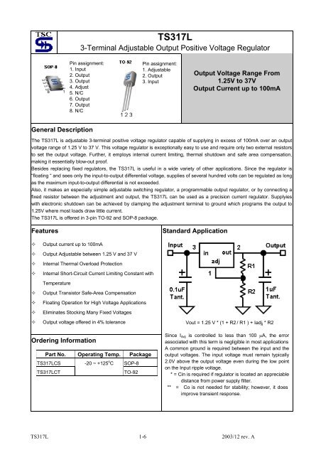
General Description<br />
TS317L<br />
3-Terminal Adjustable Output Positive Voltage Regulator<br />
Output Voltage Range From<br />
1.25V to 37V<br />
Output Current up to 100mA<br />
The TS317L is adjustable 3-terminal positive voltage regulator capable of supplying in excess of 100mA over an output<br />
voltage range of 1.25 V to 37 V. This voltage regulator is exceptionally easy to use and require only two external resistors<br />
to set the output voltage. Further, it employs internal current limiting, thermal shutdown and safe area compensation,<br />
making it essentially blow-out proof.<br />
Besides replacing fixed regulators, the TS317L is useful in a wide variety of other applications. Since the regulator is<br />
“floating “ and sees only the input-to-output differential voltage, supplies of several hundred volts can be regulated as long<br />
as the maximum input-to-output differential is not exceeded.<br />
Also, it makes an especially simple adjustable switching regulator, a programmable output regulator, or by connecting a<br />
fixed resistor between the adjustment and output, the TS317L can be used as a precision current regulator. Supplyies<br />
with electronic shutdown can be achieved by clamping the adjustment terminal to ground which programs the output to<br />
1.25V where most loads draw little current.<br />
The TS317L is offered in 3-pin TO-92 and SOP-8 package.<br />
Features<br />
Output current up to 100mA<br />
Output Adjustable between 1.25 V and 37 V<br />
Internal Thermal Overload Protection<br />
Internal Short-Circuit Current Limiting Constant with<br />
Temperature<br />
Output Transistor Safe-Area Compensation<br />
Floating Operation for High Voltage Applications<br />
Eliminates Stocking Many Fixed Voltages<br />
Output voltage offered in 4% tolerance<br />
Ordering Information<br />
Part No. Operating Temp. Package<br />
TS317LCS -20 ~ +125 SOP-8<br />
o C<br />
TS317LCT<br />
Pin assignment:<br />
1. Input<br />
2. Output<br />
3. Output<br />
4. Adjust<br />
5. N/C<br />
6. Output<br />
7. Output<br />
8. N/C<br />
TO-92<br />
Pin assignment:<br />
1. Adjustable<br />
2. Output<br />
3. Input<br />
Standard Application<br />
Vout = 1.25 V * (1 + R2 / R1 ) + Iadj j * R2<br />
Since I Adj is controlled to less than 100 µA, the error<br />
associated with this term is negligible in most applications<br />
A common ground is required between the input and the<br />
output voltages. The input voltage must remain typically<br />
2.0V above the output voltage even during the low point<br />
on the Input ripple voltage.<br />
* = Cin is required if regulator is located an appreciable<br />
distance from power supply filter.<br />
** = Co is not needed for stability; however, it does<br />
improve transient response.<br />
TS317L 1-6 2003/12 rev. A
Absolute Maximum Rating<br />
Input Voltage Vin 40 V<br />
Power Dissipation Pd Internal Limited W<br />
Operating Junction Temperature Range T J -20 ~ +125<br />
Storage Temperature Range T STG -55 ~ +150<br />
Lead Temperature (soldering 4 sec.) T LEAD +260<br />
Note: “Absolute maximum rating” indicated limits beyond which damage to the device may occur. Operating ratings<br />
indicate conditions for which the device is functional, but do not guarantee specific performance limits.<br />
Electrical Characteristics<br />
(Tj =T LOW to T HIGH see [Note 1], Vin-Vout= 5V, Io=40mA; Pmax per [Note 2]; unless otherwise specified.)<br />
CHARACTERISTIC CONDITION SYMBOL MIN. TYP. MAX. UNIT<br />
Reference voltage<br />
(Note 4)<br />
Line regulation<br />
(Note 3)<br />
Load regulation<br />
(Note 3)<br />
5mA ≤ Io ≤ 100mA<br />
3V ≤ Vi - Vo ≤ 40V<br />
Tj = 25 o C, 3V ≤ Vi -Vo ≤ 40V,<br />
Io=20mA<br />
o C<br />
o C<br />
o C<br />
Vref 1.20 1.25 1.30 V<br />
REGline -- 0.01 0.07 %/V<br />
Tj = 25 o C, 5mA ≤ I O ≤ Imax, REGload -- 0.1 1.5 %<br />
Thermal regulation Tj = 25 o C, 10 ms Pulse -- -- 0.03 0.2 %/W<br />
Adjustment pin current Iadj -- 50 100 uA<br />
Adjustment pin current<br />
change<br />
Pd ≤ Pmax, 5mA ≤ Io ≤ Imax,<br />
3V ≤ V I - V O ≤ 40V<br />
Current limit 3V ≤ V I - V O ≤ 13V<br />
V I - V O = 40V<br />
∆Iadj<br />
I LIMIT<br />
-- 0.2 5.0 uA<br />
Temperature stability T LOW ≤ Tj ≤ T HIGH T S -- 0.65 -- %<br />
Minimum load current V I - V O ≤ 40V Imin -- 3.5 5 mA<br />
RMS Noise, % of V O Ta =25 o C, 10H Z ≤ f ≤ 10KH Z N -- 0.003 -- %<br />
Ripple rejection ratio Vout= 10V, f= 120Hz, Cadj= 0 -- -- 65 -- dB<br />
Long-term stability<br />
(Note 5)<br />
Thermal resistance<br />
Junction to Ambient<br />
Tj = 125 o C, 1000hrs S -- 0.3 1.0 %<br />
CT package 0.4” leads<br />
CS package<br />
Notes:<br />
1. TLOW = -20 o C, T HIGH = + 125 o C<br />
2. Pmax: CS package=0.5W, CT package=0.625W,<br />
3. Load and line regulation are specified at constant junction temperature. Changes in output voltage due to heating<br />
effects must be taken into account separately. Pulse testing with low duty cycle is used.<br />
4. Selected devices with tightened tolerance reference voltage available.<br />
5. Since Long-Term Stability cannot be measured on each device before shipment, this specification is an engineering<br />
estimate of average stability from lot to lot.<br />
TS317L 2-6 2003/12 rev. A<br />
Rθja<br />
--<br />
--<br />
--<br />
--<br />
200<br />
50<br />
180<br />
165<br />
--<br />
--<br />
--<br />
--<br />
mA<br />
o C/W
Application Information<br />
Basic Circuit Operation<br />
The TS317L is a 3-terminal floating regulator. In<br />
operation, the TS317L develops and maintains a<br />
nominal 1.25V reference (Vref) between its output and<br />
adjustment terminals. This reference voltage is<br />
converted to a programming current (Iprog.) by R1 (see<br />
Figure 17), and this constant current flows through R2<br />
to ground. The regulated output voltage is given by:<br />
Vout = Vref ( 1 + R2 / R1 ) + Iadj * R2<br />
Since the current from the adjustment terminal (Iadj)<br />
represents an error term in the equation, the TS317L<br />
was designed to control Iadj to less than 100uA and<br />
keep it constant. To do this, all quiescent operating<br />
current is returned to the output terminal. This imposes<br />
the requirement for a minimum load current. If the load<br />
current is less than this minimum, the output voltage<br />
will rise.<br />
Since the TS317L is a floating regulator, it is only the<br />
voltage differential across the circuit which is important<br />
to performance, and operation at high voltages with<br />
respect to ground is possible.<br />
Figure 1. basic circuit configuration<br />
Load Regulation<br />
The TS317L is capable of providing extremely good<br />
load regulation, but a few precautions are needed to<br />
obtain maximum performance. The current set resistor<br />
connected between the adjustment therminal and the<br />
output terminal (usually 240Ω) should be tied directly to<br />
the output of the regulator rather than near the load.<br />
This eliminates line drops from appearing effectively in<br />
series with the reference and degrading regulation. For<br />
example, a 15V regulator with 0.05Ω resistance<br />
between the regulator and load will have a load<br />
regulation due to line resistance of 0.05Ω x Io.<br />
If the set resistor is connected near the load the<br />
effective line resistance will be 0.05Ω (1+ R2/R1) or in<br />
this case, 11.5 times worse.<br />
Figure 6 shows the effect of resistance between the<br />
regulator and 240Ω set resistor.<br />
With the TO-92 package, it is easy to minimize the<br />
resistance from the case of the set resistor, by using<br />
two separate leads to the output pin. The ground of R2<br />
can be returned near the ground of the load to provide<br />
remote ground sensing and improve load regulation.<br />
Figure 2. Regulator with line resistance in<br />
output lead<br />
External Capacitor<br />
An input bypass capacitor is recommended in case the<br />
regulator is more than 6 inches away from the usual<br />
large filter capacitor. A 0.1µF disc or 1µF tantalum<br />
input bypass capacitor (Cin) is recommended to reduce<br />
the sensitivity to input line impedance.<br />
The adjustment terminal may be bypassed to ground to<br />
improve ripple rejection and noice. This capacitor<br />
(Cadj) prevents ripple from being amplified as the<br />
output voltage is increased. With a 10uF bypass<br />
capacitor 80dB ripple rejection is obtainable at any<br />
output level. Increased over 10uF do not appreciably<br />
improve the ripple rejection at frequencies above<br />
120Hz. If the bypass capacitor is used, it is sometimes<br />
necessary to include protection diodes to prevent the<br />
capacitor from discharging through internal low current<br />
paths and damaging the device.<br />
In general, the best type of capacitors to use is solid<br />
tantalum. Solid tantalum capacitors have low<br />
impedance even at high frequencies. Depending upon<br />
capacitor construction, it takes about 25uF in aluminum<br />
electrolytic to equal 1uF solid tantalum at high<br />
frequencies. Ceramic capacitors are also good at high<br />
frequencies; but some types have a large<br />
TS317L 3-6 2003/12 rev. A
Application Information (continued)<br />
decrease in capacitance at frequencies around<br />
0.5MHz. for this reason, a 0.01uF disc may seem to<br />
work better than a 0.1uF disc as a bypass.<br />
Although the TS317L is stable with no output<br />
capacitance, like any feedback circuit, certain values of<br />
external capacitance can cause excessive ringing. This<br />
occurs with values between 50pF and 5000pF. A 1uµF<br />
solid tantalum (or 25uF aluminum electrolytic) on the<br />
output swamps this effect and insures stability.<br />
Thermal Regulation<br />
When power is dissipated in an IC, a temperature<br />
gradient occurs across the IC chip affecting the<br />
individual IC circuit components. With an IC regulator,<br />
this gradient can be especially severe since power<br />
dissipation is large. Thermal regulation is the effect of<br />
these temperature gradients on output voltage (in<br />
percentage output change) per watt of power change in<br />
a specified time. Thermal regulation error is<br />
independent of electrical regulation of temperature<br />
coefficient, and occurs within 5ms to 50ms after a<br />
change in power dissipation. Thermal regulation<br />
depends on IC layout as well as electrical design. The<br />
thermal regulation of a voltage regulator is defined as<br />
the percentage change of Vout, per watt, within the first<br />
10ms after a step of power is applied. The TS317L<br />
specification is 0.2%/W, maximum.<br />
TS317L’s output changes only 7mV (or 0.07% of Vout=<br />
-10V) when a 1W pulse is applied for 10ms. This<br />
performance is thus well inside the specification limit of<br />
0.2%/W x 1W = 0.2% maximum. When the 1W pulse is<br />
ended, the thermal regulation again shows a 7mV<br />
change as the gradients across the TS317L chip die<br />
out. Note that the load regulation error of about 14mV<br />
(0.14%) is additional to the thermal regulation error.<br />
Protection Diode<br />
When external capacitors are used with any I.C.<br />
regulator it is sometimes necessary to add protection<br />
diodes to prevent the capacitors from discharging<br />
through low current points into the regulator. Most<br />
10uF capacitors have low enough internal series<br />
resistance to deliver 20A spikes when shorted.<br />
Although the surge is short, these is enough energy to<br />
damage parts of the IC.<br />
When an output capacitor is connected to a regulator<br />
and the input is shorted, the output capacitor will<br />
Discharge into the output of the regulator. The<br />
discharge current depends on the value of the<br />
capacitor, the output voltage of the regulator, and the<br />
rate of decrease of Vin. In the TS317L, this discharge<br />
path is through a large junction that is able to sustain a<br />
2A surge with no problem. this is not true of other types<br />
of positive regulators. For output capacitors of 25uF or<br />
less, the TS317L’s ballast resistors and output<br />
structure limit the peak current to a low enough level so<br />
that there is no need to use a protection diode.<br />
The bypass capacitor on the adjustment terminal can<br />
discharge through a low current junction. Discharge<br />
occurs when either the input or output is shorted.<br />
Internal to the TS317L is a 50Ω resistor which limits the<br />
peak discharge current. No protection is needed for<br />
output voltages of 25V or less and 10uF capacitance.<br />
Figure 3 shows an TS317L with protection diodes<br />
included for use with outputs greater than 25V and high<br />
values of output capacitance.<br />
igure 3. regulator with protection diode<br />
TS317L 4-6 2003/12 rev. A<br />
F
Typical Application<br />
Digitally selected outputs<br />
Adjustable regulator with improved<br />
Ripple rejection<br />
Adjustable current limiter<br />
5V logic regulator with electronic shutdown<br />
High gain amplifier<br />
Slow turn-on 15V regulator<br />
Precision current limiter<br />
Current limited 6V charger<br />
TS317L 5-6 2003/12 rev. A
G<br />
D<br />
A<br />
A<br />
16 9<br />
1 8<br />
D<br />
B<br />
C<br />
K<br />
B<br />
H<br />
P<br />
C<br />
TO-92 Mechanical Drawing<br />
G<br />
E F<br />
DIM<br />
SOP-8 Mechanical Drawing<br />
M<br />
R<br />
F<br />
TO-92 DIMENSION<br />
MILLIMETERS INCHES<br />
MIN MAX MIN MAX<br />
A 4.30 4.70 0.169 0.185<br />
B 4.30 4.70 0.169 0.185<br />
C 14.30(typ) 0.563(typ)<br />
D 0.43 0.49 0.017 0.019<br />
E 2.19 2.81 0.086 0.111<br />
F 3.30 3.70 0.130 0.146<br />
G 2.42 2.66 0.095 0.105<br />
H 0.37 0.43 0.015 0.017<br />
DIM<br />
SOP-8 DIMENSION<br />
MILLIMETERS INCHES<br />
MIN MAX MIN MAX<br />
A 4.80 5.00 0.189 0.196<br />
B 3.80 4.00 0.150 0.157<br />
C 1.35 1.75 0.054 0.068<br />
D 0.35 0.49 0.014 0.019<br />
F 0.40 1.25 0.016 0.049<br />
G 1.27 (typ) 0.05 (typ)<br />
K 0.10 0.25 0.004 0.009<br />
M 0 o 7 o 0 o 7 o<br />
P 5.80 6.20 0.229 0.244<br />
R 0.25 0.50 0.010 0.019<br />
TS317L 6-6 2003/12 rev. A