PCIe switches with integrated instrumentation speed product ...
PCIe switches with integrated instrumentation speed product ...
PCIe switches with integrated instrumentation speed product ...

Create successful ePaper yourself
Turn your PDF publications into a flip-book with our unique Google optimized e-Paper software.
UNIT<br />
UNDERTEST<br />
INNOVATION IN ELECTRONICS TEST TECHNOLOGY<br />
of its health. Purely as a matter of<br />
convenience, similar access can be<br />
provided through the debug port<br />
to downstream devices’ control<br />
and status registers. When used<br />
in this manner, the debug processor<br />
acts like the management or<br />
service processor used in servers<br />
and, indeed, their functions may<br />
be combined.<br />
Evolution of <strong>instrumentation</strong><br />
After functional debugging, stress<br />
testing and error injection are two<br />
necessary parts of <strong>product</strong> development.<br />
A switch’s normal data<br />
path is easily modified to function<br />
as an exerciser. As a first step, the<br />
switch sets aside a portion of its<br />
buffer memory, allows software<br />
to build packets therein, and then<br />
transmits the packets on a selected<br />
link. More advanced implementations<br />
include counting, looping,<br />
and branching mechanisms to support<br />
more complex packet streams<br />
and add a pseudorandom element to the error injection.<br />
When operating some portion of a switch as an exerciser, the<br />
ports involved no longer act as <strong>switches</strong>. Therefore, this capability<br />
is not as unobtrusive as other development acceleration<br />
features found in <strong>PCIe</strong> <strong>switches</strong>. Nevertheless, the simple availability<br />
of a component that can perform error injection and generate<br />
a full wire-<strong>speed</strong> packet stream on up to an x16 Gen 2 link<br />
is a huge boon to the <strong>product</strong> validation community.<br />
Implementing embedded <strong>instrumentation</strong><br />
At PLX Technology, integrating these capabilities into <strong>PCIe</strong> silicon<br />
evolved out of a selfish desire to reduce manufacturing costs<br />
and facilitate internal debug and validation efforts. It quickly<br />
became evident that these capabilities were perhaps even more<br />
valuable to customers for the accelerative<br />
effect on their <strong>product</strong> development process.<br />
Because technology is advancing<br />
to ever-higher interconnect <strong>speed</strong>s, PLX<br />
believes that <strong>integrated</strong> <strong>instrumentation</strong><br />
is fast becoming essential, especially for<br />
<strong>PCIe</strong> <strong>switches</strong>.<br />
Implementing the SERDES eye measurement<br />
capability requires close cooperation<br />
<strong>with</strong> both SERDES and SERDES BIST<br />
intellectual property vendors, then diligent<br />
work by design teams to exploit the<br />
capabilities thus provided.<br />
Implementing on-chip logic analysis is enabled<br />
by a design methodology that requires<br />
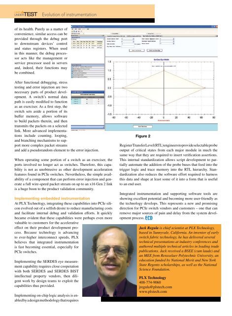
Figure 2<br />
Register Transfer Level (RTL) engineers to provide selectable probe<br />
output of critical states from each major module in much the<br />
same way that they are required to insert verification assertions.<br />
This internal standardization allows script development to partially<br />
automate the addition of the probe buses that feed into the<br />
trigger logic and trace memory into the RTL hierarchy. Standardization<br />
also reduces the software effort required to harness<br />
this data and shape at least some of it into a form that is useful<br />
to an end user.<br />
Integrated <strong>instrumentation</strong> and supporting software tools are<br />
showing excellent potential and becoming more user-friendly as<br />
the technology develops. This represents a new and promising<br />
direction for <strong>PCIe</strong> switch vendors and customers – one that can<br />
remove major sources of pain and delay from the system development<br />
process.<br />
Jack Regula is chief scientist at PLX Technology,<br />
based in Sunnyvale, California. An inventor of early<br />
switch fabric technology, he has delivered several<br />
technical presentations at industry conferences and<br />
authored multiple technical articles in leading trade<br />
publications. Jack received a BSEE (cum laude) and<br />
an MEE from Rensselaer Polytechnic University, an<br />
education funded by National Merit and New York<br />
State Regents scholarships, as well as the National<br />
Science Foundation.<br />
PLX Technology<br />
408-774-9060<br />
jregula@plxtech.com<br />
www.plxtech.com