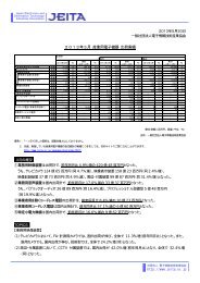
Standard of integrated circuits packages (P-ZIP) - JEITA
Standard of integrated circuits packages (P-ZIP) - JEITA
Standard of integrated circuits packages (P-ZIP) - JEITA

Create successful ePaper yourself
Turn your PDF publications into a flip-book with our unique Google optimized e-Paper software.
<strong>Standard</strong> <strong>of</strong> Japan Electronics and Information Technology Industries Association<br />
EIAJ ED-7311-17<br />
<strong>Standard</strong> <strong>of</strong> <strong>integrated</strong> <strong>circuits</strong> <strong>packages</strong><br />
(P-<strong>ZIP</strong>)<br />
Established in June, 2001<br />
Prepared by<br />
Technical <strong>Standard</strong>ization Committee on Semiconductor Device Package<br />
Published by<br />
Japan Electronics and Information Technology Industries Association<br />
11, Kanda-surugadai 3-chome, Chiyoda-ku, Tokyo 101-0062, Japan<br />
Printed in Japan
Translation without guarantee in the event <strong>of</strong> any doubt arising, the original standard in Japanese is<br />
to be evidence.<br />
<strong>JEITA</strong> standards are established independently to any existing patents on the products, materials or<br />
processes they cover.<br />
<strong>JEITA</strong> assumes absolutely no responsibility toward parties applying these standards or toward patent owners.<br />
© 2001 by the Japan Electronics and Information Technology Industries Association<br />
All rights reserved. No part <strong>of</strong> this standards may be reproduced in any form or by any means<br />
without prior permission in writing from the publisher.
EIAJ ED-7311-17<br />
<strong>Standard</strong> <strong>of</strong> Japan Electronics and Information Technology Industries Association<br />
1. Scope <strong>of</strong> Application<br />
<strong>Standard</strong> <strong>of</strong> <strong>integrated</strong> <strong>circuits</strong> package<br />
(P-<strong>ZIP</strong>)<br />
This standard covers the registered dimensions <strong>of</strong> the Zigzag Inline <strong>packages</strong>/ Shrink Zigzag Inline<br />
<strong>packages</strong>, terminal straight e pitch is 1.27mm (50mil)/ less than 0. 889mm (35 mil), among the<br />
<strong>packages</strong> classified as form C in the EIAJ ED-7300 [Recommended practice on <strong>Standard</strong> for the<br />
preparation <strong>of</strong> outline drawings <strong>of</strong> semiconductor <strong>packages</strong>]<br />
Note. This standard is the revision version to have <strong>integrated</strong> two standards into which EIAJ ED-<br />
7405 (P-<strong>ZIP</strong>) and EIAJ ED-7405-1 (P-S<strong>ZIP</strong>).<br />
2. Definition <strong>of</strong> the Technical Terms<br />
The definition <strong>of</strong> the technical terms used in this technical report is in conformity with EIAJ ED-<br />
7300, and the definition <strong>of</strong> technical terms appearing a new are given within the text <strong>of</strong> this standard.<br />
3. BACKGROUND<br />
Recently, through hole type package P-<strong>ZIP</strong> with reduced print <strong>circuits</strong> board area were developed for<br />
small size electronics devices. This technical report intended to standardize the outer dimensions <strong>of</strong> P-<br />
<strong>ZIP</strong>, P-S<strong>ZIP</strong>, and ensure compatibility between products as far as possible for standardization.<br />
4. Definition <strong>of</strong> P-<strong>ZIP</strong>/P-S<strong>ZIP</strong><br />
P-<strong>ZIP</strong>/P-S<strong>ZIP</strong> is defined as Form C in the classification <strong>of</strong> shapes <strong>of</strong> semiconductor device at the<br />
EIAJED-7300 and terminal straight pitch is 1.27mm (50mil)/ less than 0.889mm (35 mil) by<br />
bending terminal make a two lines in alternately forming leads from one package body side to a<br />
seating plane.<br />
5. Numbering <strong>of</strong> Terminals<br />
Numbering <strong>of</strong> terminals complies with the EIAJ ED-7300.<br />
6. Nominal Dimensions<br />
Package height × Package length is applied to Nominal Dimensions.<br />
(Symbol : A 2 nom × D 1 nom)<br />
- 1 -
EIAJ ED-7311-17<br />
7. REFERENCE CHARACTERS AND DRAWING<br />
7.1 Outline Drawing<br />
1 ( )<br />
Z1<br />
Z<br />
( 7 )<br />
8 ( )<br />
1<br />
6 ( )<br />
PACKAGE NAME<br />
P-<strong>ZIP</strong>/S<strong>ZIP</strong><br />
D1/3<br />
b2<br />
D<br />
D1<br />
( 4)<br />
8 ( )<br />
7 ( )<br />
INDEX<br />
AREA<br />
Figure 1<br />
5 ( )<br />
<strong>JEITA</strong> STANDARD<br />
PACKAGE OUTLINE DRAWINGS<br />
b<br />
X<br />
e<br />
M<br />
- 3 -<br />
n<br />
7<br />
( )<br />
C A B<br />
A<br />
C<br />
( 8 )<br />
A2<br />
A<br />
A1<br />
Z1<br />
Z<br />
A3<br />
3 ( )<br />
L<br />
DATE<br />
01-03-16<br />
e1<br />
5 ( )<br />
<strong>JEITA</strong> REGISTRATION NO.<br />
IC-7328-001<br />
B<br />
E<br />
b1<br />
b<br />
c<br />
0.50<br />
c1 c<br />
SHEET<br />
1/11
- 4 -<br />
EIAJ ED-7311-17<br />
Notes:<br />
( 1 ) The bending direction <strong>of</strong> terminal No.1 is in the side <strong>of</strong> the terminal No.1 index.<br />
( 2 ) The seating plane is determined when the terminal is inserted to hole that <strong>of</strong> center is located in the<br />
matrix as modulus e / e1 .<br />
( 3 ) The maximum mounting conditions apply to the positional tolerance <strong>of</strong> the terminals.(For the<br />
maximum body conditions, refer to ISO/1101, part II)<br />
( 4 ) Shows the allowable position <strong>of</strong> the index mark, which <strong>of</strong> more than half must be included in the<br />
shaded area.<br />
( 5 ) Specifies the true geometric position <strong>of</strong> the terminal axis.<br />
( 6 ) The shapes <strong>of</strong> chanfer is recommended in Figure 3.<br />
( 7 ) Resin flash, leadframe cutting remain and gate remains are not included.<br />
( 8 ) Resin flash, leadframe cutting remain and gate remains are included.<br />
PACKAGE NAME<br />
P-<strong>ZIP</strong>/S<strong>ZIP</strong><br />
φ0.8mm<br />
Figure 2<br />
<strong>JEITA</strong> STANDARD<br />
PACKAGE OUTLINE DRAWINGS<br />
e 1<br />
Seating Plane<br />
Bending Cross Point<br />
<strong>of</strong> terminal<br />
DATE<br />
01-03-16<br />
<strong>JEITA</strong> REGISTRATION NO.<br />
IC-7328-001<br />
Figure 3<br />
SHEET<br />
2/11
EIAJ ED-7311-17<br />
8. Registration table<br />
(Package name):P-<strong>ZIP</strong>/P-S<strong>ZIP</strong><br />
(Registration number): IC-7311-17-00-00.0-XX<br />
Note. The Numbers in the table indicate,<br />
(Terminal number n)-(package length D1nom)-(serial number)<br />
PACKAGE NAME<br />
P-<strong>ZIP</strong>/S<strong>ZIP</strong><br />
<strong>JEITA</strong> STANDARD<br />
PACKAGE OUTLINE DRAWINGS<br />
- 5 -<br />
Terminal pitch e<br />
Letter Code A2nom 1.27 0.889<br />
A 4.40<br />
B 5.80<br />
14-18.2-BA<br />
18-23.3-BB<br />
16-14.0-AA<br />
16-14.0-AB<br />
16-13.8-AC<br />
16-13.8-AD<br />
C 6.80 21-19.4-CA<br />
D 8.80<br />
20-25.5-DA<br />
20-25.5-DB<br />
20-30.5-DC<br />
22-30.2-DE<br />
28-36.0-DF<br />
E 10.80<br />
24-30.5-EA<br />
40-51.2-EB<br />
F 12.80 64-54.0-FA<br />
DATE<br />
01-03-16<br />
<strong>JEITA</strong> REGISTRATION NO.<br />
IC-7328-001<br />
SHEET<br />
3/11
Serial Number AA AB<br />
- 6 -<br />
EIAJ ED-7311-17<br />
External Type P-S<strong>ZIP</strong>16-4.3 × 14.0-0.89 P-S<strong>ZIP</strong>16-4.3 × 14.0-0.89<br />
Reference Symbol<br />
Group1<br />
Group2<br />
PACKAGE NAME<br />
P-<strong>ZIP</strong>/S<strong>ZIP</strong><br />
min nom max min nom max<br />
A - 5.35 - - 5.35 -<br />
A 1 - 1.00 - - 1.00 -<br />
A 2 4.35 4.35<br />
A 3 - 8.45 - - 7.65 -<br />
b 0.36 0.40 0.48 0.36 0.40 0.48<br />
b 1 0.35 0.40 0.45 0.35 0.40 0.45<br />
b 2 0.00 0.15 0.30 0.00 0.15 0.30<br />
C 0.19 0.20 0.25 0.19 0.20 0.25<br />
C 1 0.19 0.20 0.21 0.19 0.20 0.21<br />
D 13.90 14.00 14.10 13.90 14.00 14.10<br />
D 1 - 14.00 - - 14.00 -<br />
E 2.10 2.20 2.30 2.10 2.20 2.30<br />
e - 0.889 - - 0.889 -<br />
e 1 - 1.778 - - 1.778 -<br />
θ 0° 4° 8° 0° 4° 8°<br />
x - 0.23 - - 0.23 -<br />
n - 16 - - 16 -<br />
Z - 0.61 - - 0.61 -<br />
Z 1 - 0.508 - - 0.508 -<br />
L 2.75 3.00 3.25 1.95 2.20 2.45<br />
<strong>JEITA</strong> STANDARD<br />
PACKAGE OUTLINE DRAWINGS<br />
DATE<br />
01-03-16<br />
<strong>JEITA</strong> REGISTRATION NO.<br />
IC-7328-001<br />
SHEET<br />
4/11
EIAJ ED-7311-17<br />
Serial Number AC AD<br />
External Type P-S<strong>ZIP</strong>16-4.35 × 13.8-0.89 P-S<strong>ZIP</strong>16-4.35 × 13.8-0.89<br />
Reference Symbol min nom max min nom max<br />
Group1<br />
Group2<br />
PACKAGE NAME<br />
P-<strong>ZIP</strong>/S<strong>ZIP</strong><br />
A 5.08 5.40 5.715 5.08 5.40 5.715<br />
A 1 0.95 1.10 1.25 0.95 1.10 1.25<br />
A 2 4.25 4.35 4.45 4.25 4.35 4.45<br />
A 3 7.62 8.50 9.779 7.62 7.70 9.779<br />
b 0.30 0.40 0.45 0.30 0.40 0.45<br />
b 1 0.35 0.40 0.45 0.35 0.40 0.45<br />
b 2 0.20 0.25 0.30 0.20 0.25 0.30<br />
C 0.15 0.20 0.30 0.15 0.20 0.30<br />
C 1 0.15 0.20 0.25 0.15 0.20 0.25<br />
D 13.9 14.0 14.4 13.9 14.0 14.4<br />
D 1 13.7 13.8 14.2 13.7 13.8 14.2<br />
E 2.10 2.20 2.30 2.10 2.20 2.30<br />
e - 0.889 - - 0.889 -<br />
e 1 - 1.778 - - 1.778 -<br />
θ 0° 4° 8° 0° 4° 8°<br />
x - - 0.25 - - 0.25<br />
n - 16 - - 16 -<br />
Z - 0.33 - - 0.33 -<br />
Z 1 - 0.23 - - 0.23 -<br />
L 2.85 3.10 3.35 2.05 2.30 2.55<br />
<strong>JEITA</strong> STANDARD<br />
PACKAGE OUTLINE DRAWINGS<br />
- 7 -<br />
DATE<br />
01-03-16<br />
<strong>JEITA</strong> REGISTRATION NO.<br />
IC-7328-001<br />
SHEET<br />
5/11
Serial Number BA BB<br />
External Type P-<strong>ZIP</strong>14-6.0 × 18.2-1.27 P-<strong>ZIP</strong>18-6.0 × 23.3-1.27<br />
Reference Symbol<br />
Group1<br />
Group2<br />
PACKAGE NAME<br />
P-<strong>ZIP</strong>/S<strong>ZIP</strong><br />
- 8 -<br />
EIAJ ED-7311-17<br />
min nom max min nom max<br />
A 7.76 8.26 8.76 7.76 8.26 8.76<br />
A 1 1.76 2.26 2.76 1.76 2.26 2.76<br />
A 2 5.7 6.0 6.3 5.7 6.0 6.3<br />
A 3 10.56 11.26 11.76 10.56 11.26 11.76<br />
b 0.40 0.50 0.60 0.40 0.50 0.60<br />
b 1 0.45 0.50 0.55 0.45 0.50 0.55<br />
b 2 0.20 0.25 0.35 0.20 0.25 0.35<br />
C 0.20 0.25 0.35 0.20 0.25 0.35<br />
C 1 0.20 0.25 0.35 0.20 0.25 0.35<br />
D 17.9 18.2 18.5 23.0 23.3 23.6<br />
D 1 18.0 18.2 18.4 23.1 23.3 23.5<br />
E 2.7 3.0 3.3 2.7 3.0 3.3<br />
e - 1.27 - - 1.27 -<br />
e 1 - 2.54 - - 2.54 -<br />
θ 0° 4° 8° 0° 4° 8°<br />
x - - 0.25 - - 0.25<br />
n - 14 - - 18 -<br />
Z - 0.895 - - 0.895 -<br />
Z 1 - 0.865 - - 0.865 -<br />
L 2.5 3.0 3.5 2.5 3.0 3.5<br />
<strong>JEITA</strong> STANDARD<br />
PACKAGE OUTLINE DRAWINGS<br />
DATE<br />
01-03-16<br />
<strong>JEITA</strong> REGISTRATION NO.<br />
IC-7328-001<br />
SHEET<br />
6/11
EIAJ ED-7311-17<br />
Serial Number CA<br />
External Type P-S<strong>ZIP</strong>21-6.3 × 19.4-0.89<br />
Reference Symbol min nom max<br />
Group1<br />
Group2<br />
PACKAGE NAME<br />
P-<strong>ZIP</strong>/S<strong>ZIP</strong><br />
A 8.03<br />
A 1 0.93 1.23 1.53<br />
A 2 6.10 6.30 6.50<br />
A 3<br />
- 9 -<br />
11.33<br />
b 0.35 0.45 0.55<br />
b 1 0.40 0.45 0.50<br />
b 2 0.20 0.25 0.30<br />
C 0.20 0.25 0.35<br />
C 1 0.20 0.25 0.30<br />
D 19.90<br />
D 1 19.20 19.40 19.60<br />
E 3.00 3.20 3.40<br />
e 0.889<br />
e 1<br />
2.54<br />
θ 0° 4° 8°<br />
x 0.25<br />
n 21<br />
Z 0.96<br />
Z 1<br />
0.81<br />
L 2.70 3.00 3.30<br />
<strong>JEITA</strong> STANDARD<br />
PACKAGE OUTLINE DRAWINGS<br />
DATE<br />
01-03-16<br />
<strong>JEITA</strong> REGISTRATION NO.<br />
IC-7328-001<br />
SHEET<br />
7/11
Serial Number DA DB<br />
- 10 -<br />
EIAJ ED-7311-17<br />
External Type P-<strong>ZIP</strong>20-8.5 × 25.5-1.27 P-<strong>ZIP</strong>20-8.96 × 25.5-1.27<br />
Reference Symbol min nom max min nom max<br />
Group1<br />
Group2<br />
PACKAGE NAME<br />
P-<strong>ZIP</strong>/S<strong>ZIP</strong><br />
A 9.53 9.80 10.16 9.53 9.80 10.16<br />
A 1 0.76 1.30 1.86 0.76 0.85 1.00<br />
A 2 8.30 8.50 8.80 8.66 8.96 9.26<br />
A 3 12.63 13.10 13.66 12.61 13.11 13.61<br />
b 0.44 0.52 0.60 0.44 0.52 0.60<br />
b 1 0.47 0.52 0.57 0.47 0.52 0.57<br />
b 2 0.15 0.25 0.35 0.15 0.25 0.35<br />
C 0.19 0.27 0.35 0.14 0.22 0.30<br />
C 1 0.22 0.27 0.32 0.17 0.22 0.27<br />
D 25.25 25.50 25.75 25.25 25.50 25.75<br />
D 1 25.35 25.50 25.65 25.35 25.50 25.65<br />
E 2.65 2.80 2.95 2.65 2.80 2.95<br />
e - 1.27 - - 1.27 -<br />
e 1 - 2.54 - - 2.54 -<br />
θ 0° 4° 8° 0° 4° 8°<br />
x - - 0.25 - - 0.25<br />
n - 20 - - 20 -<br />
Z - 0.685 - - 0.685 -<br />
Z 1 - 0.685 - - 0.685 -<br />
L 3.10 3.30 3.50 3.10 3.30 3.50<br />
<strong>JEITA</strong> STANDARD<br />
PACKAGE OUTLINE DRAWINGS<br />
DATE<br />
01-03-16<br />
<strong>JEITA</strong> REGISTRATION NO.<br />
IC-7328-001<br />
SHEET<br />
8/11
EIAJ ED-7311-17<br />
Serial Number DC DE<br />
External Type P-<strong>ZIP</strong>20-8.5 × 30.5-1.27 P-<strong>ZIP</strong>22-8.5 × 30.2-1.27<br />
Reference Symbol min nom max min nom max<br />
Group1<br />
Group2<br />
PACKAGE NAME<br />
P-<strong>ZIP</strong>/S<strong>ZIP</strong><br />
A 9.53 9.80 10.16 9.70 9.80 10.30<br />
A 1 0.90 1.10 1.30 1.30 1.80 2.30<br />
A 2 8.30 8.50 8.80 8.40 8.50 8.60<br />
A 3 12.40 12.90 13.40 12.85 13.20 13.95<br />
b 0.44 0.52 0.60 0.45 0.50 0.65<br />
b 1 0.47 0.52 0.57 0.45 0.50 0.55<br />
b 2 0.15 0.25 0.35 0.20 0.25 0.30<br />
C 0.19 0.27 0.35 0.20 0.25 0.40<br />
C 1 0.22 0.27 0.32 0.20 0.25 0.30<br />
D 30.25 30.50 30.75 30.15 30.40 30.65<br />
D 1 30.35 30.50 30.65 30.10 30.20 30.30<br />
E 2.65 2.80 2.95 2.90 3.00 3.10<br />
e - 1.27 - - 1.27 -<br />
e 1 - 2.54 - - 2.54 -<br />
θ 0° 4° 8° 0° 4° 8°<br />
x - - 0.25 - - 0.25<br />
n - 20 - - 22 -<br />
Z - 3.185 - - 1.87 -<br />
Z 1 - 3.185 - - 1.77 -<br />
L 3.10 3.30 3.50 3.15 3.40 3.65<br />
<strong>JEITA</strong> STANDARD<br />
PACKAGE OUTLINE DRAWINGS<br />
- 11 -<br />
DATE<br />
01-03-16<br />
<strong>JEITA</strong> REGISTRATION NO.<br />
IC-7328-001<br />
SHEET<br />
9/11
Serial Number EA EB<br />
- 12 -<br />
EIAJ ED-7311-17<br />
External Type P-<strong>ZIP</strong>24-10.7 × 30.5-1.27 P-<strong>ZIP</strong>40-10.7 × 51.2-1.27<br />
Reference Symbol min nom max min nom max<br />
Group1<br />
Group2<br />
PACKAGE NAME<br />
P-<strong>ZIP</strong>/S<strong>ZIP</strong><br />
A 11.40 11.70 12.00 11.40 11.70 12.00<br />
A 1 0.80 1.00 1.20 0.80 1.00 1.20<br />
A 2 10.40 10.70 11.00 10.40 10.70 11.00<br />
A 3 14.50 15.00 15.50 14.50 15.00 15.50<br />
b 0.44 0.52 0.60 0.44 0.52 0.60<br />
b 1 0.47 0.52 0.57 0.47 0.52 0.57<br />
b 2 0.15 0.25 0.35 0.15 0.25 0.35<br />
C 0.19 0.27 0.35 0.19 0.27 0.35<br />
C 1 0.22 0.27 0.32 0.22 0.27 0.32<br />
D 30.25 30.50 30.75 49.95 51.20 51.45<br />
D 1 30.35 30.50 30.65 50.05 51.20 51.35<br />
E 2.65 2.80 2.95 2.65 2.80 2.95<br />
e - 1.27 - - 1.27 -<br />
e 1 - 2.54 - - 2.54 -<br />
θ 0° 4° 8° 0° 4° 8°<br />
x - - 0.25 - - 0.25<br />
n - 24 - - 40 -<br />
Z - 0.645 - - 0.835 -<br />
Z 1 - 0.645 - - 0.835 -<br />
L 3.10 3.30 3.50 3.10 3.30 3.50<br />
<strong>JEITA</strong> STANDARD<br />
PACKAGE OUTLINE DRAWINGS<br />
DATE<br />
01-03-16<br />
<strong>JEITA</strong> REGISTRATION NO.<br />
IC-7328-001<br />
SHEET<br />
10/11
EIAJ ED-7311-17<br />
Serial Number DE FA<br />
External Type P-<strong>ZIP</strong>22-8.5 × 30.2-1.27 P-S<strong>ZIP</strong>64-13.75 × 54-0.82<br />
Reference Symbol min nom max min nom max<br />
Group1<br />
Group2<br />
PACKAGE NAME<br />
P-<strong>ZIP</strong>/S<strong>ZIP</strong><br />
A 9.70 9.80 10.30 16.30<br />
A 1 1.30 1.80 2.30 2.00<br />
A 2 8.40 8.50 8.60 13.60 13.75 13.90<br />
A 3 12.85 13.20 13.95 19.10<br />
b 0.45 0.50 0.65 0.30 0.40 0.50<br />
b 1 0.45 0.50 0.55 0.35 0.40 0.45<br />
b 2 0.20 0.25 0.30 0.20 0.25 0.30<br />
C 0.20 0.25 0.40 0.20 0.25 0.35<br />
C 1 0.20 0.25 0.30 0.20 0.25 0.30<br />
D 30.15 30.40 30.65 54.50<br />
D 1 30.10 30.20 30.30 53.80 54.00 54.20<br />
E 2.90 3.00 3.10 3.45 3.55 3.65<br />
e - 1.27 - 0.82<br />
e 1 - 2.54 - 2.54<br />
θ 0° 4° 8° 0° 4° 8°<br />
x - - 0.25 0.25<br />
n - 22 - 64<br />
Z - 1.87 - 1.32<br />
Z 1 - 1.77 - 1.17<br />
L 3.15 3.40 3.65 2.30 2.60 2.90<br />
<strong>JEITA</strong> STANDARD<br />
PACKAGE OUTLINE DRAWINGS<br />
- 13 -<br />
DATE<br />
01-03-16<br />
<strong>JEITA</strong> REGISTRATION NO.<br />
IC-7328-001<br />
SHEET<br />
11/11
- 14 -<br />
EIAJ ED-7311-17
EIAJ ED-7311-17<br />
COMMITTEE MEMBERS<br />
The Peripheral Package Subcommittee <strong>of</strong> the Technical <strong>Standard</strong>ization Committee on<br />
Semiconductor Device Packages has mainly deliberated this standard.<br />
The subcommittee members are shown below.<br />
<br />
Chairman ELPIDA MEMORY,INC. Ichiro Anjo<br />
<br />
Chief SANYO ELECTRIC CORP. Hideyuki Iwamura<br />
Co-chief SHARP CORP. Katuyuki Tarui<br />
FUJITSU LTD. Fumihiko Taniguchi<br />
TOSHIBA CORP. Yasuhiro Koshio<br />
MATSUSHITA ELECTRIC INDUSTRIAL CO.,LTD. Toshiyuki Fukuda<br />
Members AMKOR TECHNOROGY JAPAN.INC Naomichi Shoji<br />
ENPLAS CORP. Yoshiyuki Ohashi<br />
ENPLAS CORP. Hisao Oshima<br />
OKI ELECTRONICS INDUSTRY CO.,LTD. Kazuhiko Sera<br />
KYOCERA CORP. Akihiro Funahashi<br />
KOGUNEX Takahiro Aoki<br />
SANYO ELECTRIC CORP. Kiyoshi Mita<br />
SUMITOMO 3M CORP. Akiko Tsubota<br />
SEIKO EPSON CORP. Yoshiaki Emoto<br />
SONY CORP. Hiroshi Abe<br />
TOSHIBA CORP. Morihiko Ikemizu<br />
NEC CORP. Kaoru Sonobe<br />
NEC CORP. Kenichi Kurihara<br />
IBM JAPAN CORP. Tuneo Kobayashi<br />
TEXAS INSTRUMENTS JAPAN LTD. Kenji Masumoto<br />
NGK CORP. Katsuaki Sugino<br />
HITACHI LTD. Yoshinori Miyaki<br />
HITACHI Cable LTD. Tadashi Kawanobe<br />
FUJITSU LTD. Kaoru Tachibana<br />
FUJI ELECTRIC CO.,LTD. Osamu Hirohashi<br />
MATSUSHITA ELECTRIC INDUSTRIAL CO.,LTD. Tomoki Tamaki<br />
MITSUBISHI ELECTRIC CORP. Kazuya Fukuhara<br />
MELCO INC. Tsuneo Watanabe<br />
YAMAICHI ELECTRIC CO.,LTD. Noriyuki Matsuoka<br />
UNITECHNO INC. Hitoshi Matsunaga<br />
ROHM CO.,LTD. Osamu Miyata<br />
Special Members SHIN-ETSU POLYMER Ken Tamura<br />
TOYOJUSHI CO.,LTD. Hitoshi Kazuma<br />
- 15 -