Piezoelectric aluminium nitride thin films by PECVD - Epublications ...
Piezoelectric aluminium nitride thin films by PECVD - Epublications ...
Piezoelectric aluminium nitride thin films by PECVD - Epublications ...

Create successful ePaper yourself
Turn your PDF publications into a flip-book with our unique Google optimized e-Paper software.
UNIVERSIDAD DE LA REPÚBLICA ORIENTAL DEL URUGUAY<br />
UNIVERSITÉ DE LIMOGES (FRANCE)<br />
CO-ADVISED THESIS<br />
For the degree<br />
DOCTOR EN INGENIERÍA QUÍMICA<br />
de la Facultad de Ingeniería de MONTEVIDEO<br />
DOCTEUR DE L’UNIVERSITÉ DE LIMOGES<br />
Spécialité: Matériaux Céramiques et Traitements de Surface<br />
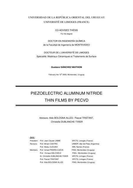
Gustavo SÁNCHEZ MATHON<br />
February the 12 th 2009, Montevideo, Uruguay<br />
PIEZOELECTRIC ALUMINUM NITRIDE<br />
Jury :<br />
THIN FILMS BY <strong>PECVD</strong><br />
Advisors: Aldo BOLOGNA ALLES / Pascal TRISTANT,<br />
Christelle DUBLANCHE-TIXIER<br />
President : Prof. Jean Claude LABBE SPCTS, Limoges (France)<br />
Revisors: Prof. Miriam CASTRO UNMDP, Mar del Plata (Argentina)<br />
Prof. Abdou DJOUADI IMN, Nantes (France)<br />
Members: Prof. Ismael PIEDRA-CUEVA FING, Montevideo (Uruguay)<br />
Prof. Enrique DALCHIELE FING, Montevideo (Uruguay)<br />
Dr. Christelle DUBLANCHE-TIXIER SPCTS, Limoges (France)<br />
Prof. Pascal TRISTANT SPCTS, Limoges (France)<br />
Prof. Aldo BOLOGNA ALLES FING, Montevideo (Uruguay)
- 2 -<br />
Acknowledgments<br />
I want to express my sincere gratitude to my thesis advisors, Dr. Aldo Bologna Alles,<br />
Dr. Pascal Tristant and Dr. Christelle Dublanche-Tixier for their friendship and<br />
guidance throughout the course of this work.<br />
I also gratefully acknowledge Dr. Jean Claude Labbe, Dr. Ismael Piedra-Cueva,<br />
Dr. Abdou Djouadi, Dr. Miriam Castro, and Dr. Enrique Dalchiele for serving on my<br />
committee.<br />
I would also like to thank to several members of the SPCTS laboratory at Limoges<br />
for their support: Daniel Tetard, Thérèse Merle, Valérie Coudert, Phillippe Thomas,<br />
Alexandre Boulle, René Guinebretiere, Bernard Soulestin, Fabrice Rossignol, Daniel<br />
Merle and Cédric Jaoul. I would like to give a special acknowledge in this sense to<br />
Hervé Hidalgo.<br />
I want to acknowledge to Jaume Esteve and Joseph Montserrat from the Instituto<br />
de Microelectrónica de Barcelona for their assistance in the cleanroom fabrication of<br />
SAW devices, as well as to Aurelian Crunteanu from X-LIM (Limoges) for his<br />
assistance in the cleanroom fabrication of BAW devices as well in the device<br />
characterizations.<br />
Furthermore, I would like to thank Florent Tetard (Université Paris XIII) as well as<br />
Bassam Abdallah, Eric Gautron, Vincent Fernandez and Jonathan Ahmon (Institut<br />
des Matériaux de Nantes) <strong>by</strong> their assistance in other characterizations.<br />
I would like to remember the rest of the PhD students at Limoges for their<br />
friendship and their hospitality: Salman Asad, Christophe Cibert, Sébastien<br />
Menessier, Béatrice Sourd, Hamid Belghazi, Claire Tendero, Aure Arcondeguy,<br />
Cécile Marchand, Olivier Tingaud and Fabrice Goutier.
I want to remember Dr. Jean Desmaison, who was my advisor at the beginning of<br />
this work, and acknowledge his wife, Dr. Martine Desmaison-Brut for her friendship<br />
during my stages at Limoges.<br />
I want to express my gratitude to all the institutions that have support this work in<br />
different ways: the University of Limoges, the University of the Republic (Uruguay)<br />
and the French Embassy in Uruguay. Particularly, I want to thank some persons of<br />
these institutions <strong>by</strong> their special disposition: Gaëlle Peyrat and Graciela Vigo.<br />
Lastly and most importantly, I would like to thank my family. I thank my wife Isabel<br />
and my son Daniel for their role in helping me attain this goal.<br />
- 3 -
Abstract<br />
Polycrystalline aluminum <strong>nitride</strong> <strong>thin</strong> <strong>films</strong> were produced with a microwave-plasma<br />
enhanced chemical vapor deposition technique. The plasma-injector distance, the<br />
substrate temperature and the RF bias were the main variables which allowed<br />
achieving this objective. At the time, it was possible to control the preferential<br />
orientation as or , both interesting for piezoelectric applications. The<br />
growth mechanisms that conducted to film microstructure development under<br />
different process conditions were explained, enriched <strong>by</strong> the comparison with a<br />
physical vapor deposition sputtering technique. The obtained <strong>films</strong> were<br />
characterized in their piezoelectric performance, including the construction of surface<br />
acoustic wave devices and bulk acoustic wave devices. Adequate piezoelectric<br />
response and acoustic velocities were obtained for oriented <strong>films</strong>, while<br />
oriented <strong>films</strong> did not show piezoelectric response under the configurations<br />
essayed. An extensive analysis was done in order to explain these behaviors.<br />
Keywords: aluminum <strong>nitride</strong>, <strong>thin</strong> <strong>films</strong>, <strong>PECVD</strong>, film microstructure, piezoelectricity,<br />
SAW devices, BAW devices.<br />
- 4 -
Resumen<br />
Películas delgadas policristalinas de nitruro de aluminio fueron producidas<br />
empleando una técnica de deposición química en fase vapor asistida por plasma de<br />
microondas. La distancia plasma - inyector, la temperatura de substrato y la<br />
polarización RF del porta-substrato fueron las principales variables que permitieron<br />
alcanzar ese objetivo. Al mismo tiempo, fue posible controlar la orientación<br />
preferencial como o , ambas de interés para aplicaciones<br />
piezoeléctricas. Los mecanismos de crecimiento que condujeron al desarrollo de la<br />
microestructura en las diferentes condiciones fueron explicados. Esta explicación fue<br />
enriquecida por la comparación con una técnica de deposición física en fase vapor<br />
por pulverización catódica. Las películas obtenidas fueron caracterizadas en su<br />
desempeño piezoeléctrico, incluyendo la construcción de dispositivos<br />
electroacústicos de onda de superficie y de onda de volumen. Las películas<br />
orientadas mostraron respuesta piezoeléctrica y velocidad de onda acústica<br />
adecuadas. Por otro lado, las películas orientadas no mostraron respuesta<br />
piezoeléctrica para las configuraciones ensayadas. Un análisis extenso fue<br />
efectuado para explicar las posibles razones de estos comportamientos.<br />
Palabras clave: nitruro de aluminio, películas delgadas, <strong>PECVD</strong>, microestructura de<br />
películas delgadas, piezoelectricidad, dispositivos SAW, dispositivos BAW.<br />
- 5 -
Résumé<br />
Des couches minces polycristallines de nitrure d’<strong>aluminium</strong> ont été produites en<br />
utilisant une technique de dépôt chimique en phase vapeur assisté par plasma<br />
micro-onde. La distance plasma - injecteur, la température du substrat et la<br />
polarisation RF du porte - substrat ont été les principales variables pour arriver à ce<br />
but. Dans un même temps, il a été possible de contrôler l’orientation préférentielle<br />
comme ou , intéressantes pour des applications piézoélectriques.<br />
Les mécanismes de croissance qui ont conduit au développement des<br />
microstructures dans les différentes conditions ont été expliqués, la comparaison<br />
avec une technique de dépôt physique en phase vapeur par pulvérisation cathodique<br />
a permis d’enricher la discussion. Les performances piézoélectriques des couches<br />
obtenues ont été caractérisées par construction des dispositifs électroacoustiques<br />
d’onde de surface et d’onde de volume. Les couches orientées ont montré<br />
une réponse piézoélectrique et une vitesse acoustique adéquates. Par contre, les<br />
couches orientées n’ont pas montré de réponse piézoélectrique dans les<br />
configurations testées. Une analyse exhaustive a été conduite pour expliquer les<br />
possibles raisons de ces comportements.<br />
Mots-clés : nitrure d’<strong>aluminium</strong>, couches minces, <strong>PECVD</strong>, microstructure,<br />
piézoélectricité, dispositifs SAW, dispositifs BAW.<br />
- 6 -
Contents<br />
INTRODUCTION...................................................................................................... 14<br />
Chapter 1.................................................................................................................. 16<br />
PIEZOELECTRIC ALUMINUM NITRIDE THIN FILMS: FUNDAMENTALS AND<br />
STATE OF THE ART ............................................................................................ 16<br />
1.1 <strong>Piezoelectric</strong>ity ............................................................................................ 16<br />
1.1.1 Applications of the piezoelectric effect.................................................. 19<br />
1.1.2 Bulk acoustic wave devices .................................................................. 21<br />
1.1.3 Surface acoustic wave devices............................................................. 23<br />
1.1.4 Characteristics of piezoelectric film for electro-acoustic devices........... 24<br />
1.1.5 <strong>Piezoelectric</strong> materials .......................................................................... 27<br />
1.2 Aluminum Nitride ......................................................................................... 29<br />
1.2.1 AlN <strong>films</strong> for BAW and SAW electro-acoustic devices .......................... 34<br />
1.3 Thin Film Manufacturing Techniques........................................................... 37<br />
1.3.1 Plasma assisted techniques for <strong>thin</strong> <strong>films</strong> deposition............................ 38<br />
1.3.2 Plasma assisted techniques for polycrystalline AlN <strong>films</strong>...................... 41<br />
1.4 Thin Film Growth Mechanisms .................................................................... 44<br />
1.4.1 Development of preferential orientation in AlN <strong>thin</strong> <strong>films</strong>....................... 46<br />
1.4.2 Residual stress in <strong>thin</strong> <strong>films</strong> .................................................................. 50<br />
1.5 Objectives.................................................................................................... 52<br />
Chapter 2.................................................................................................................. 53<br />
EXPERIMENTAL PROCEDURE .......................................................................... 53<br />
2.1 The MW<strong>PECVD</strong> technique......................................................................... 53<br />
2.1.1 The reactor ........................................................................................... 53<br />
2.1.2 The process .......................................................................................... 55<br />
2.1.3 Experimental design ............................................................................. 56<br />
2.2 Film characterization ................................................................................... 57<br />
2.2.1 Chemical composition........................................................................... 58<br />
2.2.2 Microstructure ....................................................................................... 60<br />
2.2.3 Mechanical properties........................................................................... 63<br />
2.2.4 <strong>Piezoelectric</strong> Characterization............................................................... 64<br />
- 7 -
2.3 Plasma characterization <strong>by</strong> Optical Emission Spectroscopy (OES) ............ 68<br />
Chapter 3.................................................................................................................. 69<br />
GROWTH OF POLYCRYSTALLINE ORIENTED AlN FILMS............................... 69<br />
3.1 Plasma-injector distance ............................................................................. 70<br />
3.2 RF-bias........................................................................................................ 73<br />
3.3 Substrate temperature................................................................................. 74<br />
3.4 Chamber total pressure............................................................................... 76<br />
3.5 Injector-substrate distance .......................................................................... 78<br />
3.6 Process time................................................................................................ 80<br />
3.7 Film Substrates ........................................................................................... 80<br />
3.8 Discussion................................................................................................... 83<br />
Chapter 4.................................................................................................................. 85<br />
OPTMIZATION OF FILM PROPERTIES .............................................................. 85<br />
4.1 Pressure-temperature combined effect ....................................................... 85<br />
4.1.1 Annealing effect .................................................................................... 89<br />
4.1.2 Intrinsic stresses vs. temperature for oriented <strong>films</strong>................. 90<br />
4.1.3 <strong>Piezoelectric</strong> coefficient vs. temperature and pressure......................... 92<br />
4.2 Evolution of film properties with thickness................................................... 93<br />
4.2.1 Microstructure evolution in film profile................................................... 96<br />
4.2.2 <strong>Piezoelectric</strong> coefficient vs. thickness................................................... 99<br />
4.3 Effect of low RF bias potentials ................................................................... 99<br />
4.3.1 Development of thicker <strong>films</strong>............................................................... 106<br />
4.4 Effect of the H2 addition to the reaction chamber....................................... 108<br />
4.5 Optimal process conditions ....................................................................... 109<br />
4.5.1 Reproducibility of the MW<strong>PECVD</strong> technique ...................................... 113<br />
4.6 Effect of process parameters on plasma characteristics ........................... 114<br />
4.6.1 Identification of species present in the plasma ................................... 115<br />
4.6.2 Effect of H2 addition ............................................................................ 115<br />
4.6.3 Characterization of process plasmas in optimal conditions................. 117<br />
Chapter 5................................................................................................................ 121<br />
APPLICATION TO ELECTROACOUSTIC DEVICES ......................................... 121<br />
5.1 SAW devices ............................................................................................. 121<br />
5.1.1 Frequency response ........................................................................... 121<br />
- 8 -
5.1.2 Modeled response .............................................................................. 125<br />
5.2 BAW devices ............................................................................................. 127<br />
5.2.1 Frequency response ........................................................................... 128<br />
5.2.2 Modeled response .............................................................................. 128<br />
5.3 Discussion................................................................................................. 130<br />
Chapter 6................................................................................................................ 134<br />
COMPARISON WITH A PVD TECHNIQUE........................................................ 134<br />
6.1 PVD sputtering .......................................................................................... 134<br />
6.2 <strong>Piezoelectric</strong> performance......................................................................... 136<br />
6.3 Discussion................................................................................................. 139<br />
CONCLUSIONS ..................................................................................................... 142<br />
Future Work............................................................................................................ 147<br />
References ............................................................................................................. 148<br />
Appendix A ............................................................................................................. 163<br />
BAW AND SAW DEVICES ................................................................................. 163<br />
A.1 BAW devices............................................................................................. 163<br />
A.2 SAW devices............................................................................................. 171<br />
Appendix B ............................................................................................................. 178<br />
PIEZOELECTRIC CHARACTERIZATION OF THIN FILMS ............................... 178<br />
B.1 Quasi-static measurements ...................................................................... 178<br />
B.2 Dynamic measurements ........................................................................... 186<br />
Appendix C............................................................................................................. 187<br />
A MODEL OF THE ELECTRIC FIELD UNDER THE ELECTRODES................. 187<br />
C.1 The problem.............................................................................................. 187<br />
C.2 Fundamental Equations............................................................................ 188<br />
C.3 Finite differences method.......................................................................... 188<br />
C.4 Results...................................................................................................... 190<br />
Resumen ejecutivo ................................................................................................. 193<br />
PELÍCULAS DELGADAS PIEZOELECTRICAS DE NITRURO DE ALUMINIO POR<br />
<strong>PECVD</strong>................................................................................................................ 193<br />
Résumé étendu ...................................................................................................... 205<br />
COUCHES MINCES PIEZOELECTRIQUES DE NITRURE D’ALUMINIUM PAR<br />
<strong>PECVD</strong>................................................................................................................ 205<br />
- 9 -
List of Tables<br />
Table 1.1: Properties of piezoelectric materials........................................................ 28<br />
Table 2.1: Variables of the <strong>PECVD</strong> depositions process.......................................... 56<br />
Table 4.1: <strong>Piezoelectric</strong> coefficients for AlN <strong>films</strong>: temperature and pressure .......... 92<br />
Table 4.2: <strong>Piezoelectric</strong> coefficients for AlN <strong>films</strong>: thickness and temperature ......... 99<br />
Table 4.3: <strong>Piezoelectric</strong> coefficient of AlN <strong>films</strong>: RF bias potential. ........................ 106<br />
Table 4.4: <strong>Piezoelectric</strong> coefficients for AlN <strong>films</strong>: RF bias potential and thickness 107<br />
Table 4.5: Optimal process conditions for AlN <strong>films</strong> deposition .............................. 109<br />
Table 4.6: RBS / NRA analysis of AlN <strong>films</strong> at the optimal process conditions....... 112<br />
Table 5.1: Estimation of AlN film properties............................................................ 126<br />
- 10 -
List of Figures<br />
Figure 1.1: FBAR and SMR bulk acoustic wave devices.......................................... 22<br />
Figure 1.2: Surface acoustic wave device ................................................................ 23<br />
Figure 1.3: Wurtzite type structure of AlN................................................................. 30<br />
Figure 1.4: <strong>Piezoelectric</strong>ity in an aluminum <strong>nitride</strong> crystal. ....................................... 33<br />
Figure 1.5: Different possible orientations of AlN <strong>films</strong> . ........................................... 35<br />
Figure 1.6: Representation of inversion domains in the film ..................................... 36<br />
Figure 1.7: PAPVD and <strong>PECVD</strong> processes.............................................................. 41<br />
Figure 1.8: Chemical Vapor Deposition film growth.................................................. 43<br />
Figure 1.9: Basic modes of <strong>thin</strong> film growth.............................................................. 45<br />
Figure 1.10: Structure-zone diagrams (SZDs).......................................................... 46<br />
Figure 1.11: Nucleation density model ..................................................................... 48<br />
Figure 1.12: Dimmer model ...................................................................................... 49<br />
Figure 2.1: The MW<strong>PECVD</strong> reactor. ........................................................................ 54<br />
Figure 2.2: X-ray diffraction configuration................................................................. 61<br />
Figure 2.3: PFM setup to evaluate the d33 piezoelectric coefficient.. ........................ 65<br />
Figure 2.4: Scheme of the process to obtain the SAW devices................................ 66<br />
Figure 2.5: Scheme of the process to obtain BAW devices...................................... 67<br />
Figure 3.1: XRD patterns for AlN <strong>films</strong>: effect of plasma-injector distance ............... 71<br />
Figure 3.2: FTIR spectra for AlN <strong>films</strong> : effect of plasma-injector distance.. ............. 72<br />
Figure 3.3: AFM images spectra for AlN <strong>films</strong>: effect of plasma-injector distance .... 72<br />
Figure 3.4: XRD patterns and FTIR partial spectra: effect of RF bias potential ....... 73<br />
Figure 3.5: SEM micrographs of AlN <strong>films</strong>: effect of RF bias potential. ................... 74<br />
Figure 3.6: XRD patterns and FTIR partial spectra : effect of temperature............... 75<br />
Figure 3.7: AFM images of the AlN film: effect of temperature. ................................ 76<br />
Figure 3.8: XRD patterns and FTIR partial spectra: effect of pressure..................... 77<br />
Figure 3.9: AFM images and SEM micrographs of AlN <strong>films</strong>: pressure 8 Pa............ 78<br />
Figure 3.10: Deposition rate vs. injector-substrate distance. .................................... 79<br />
Figure 3.11: XRD patterns for AlN <strong>films</strong>: injector–substrate distance ....................... 79<br />
Figure 3.12: XRD patterns for <strong>films</strong> deposited on Pt(111) ........................................ 81<br />
Figure 3.13: XRD patterns AlN <strong>films</strong> deposited on Si(100) and Si(111). .................. 82<br />
- 11 -
Figure 3.14: TEM micrograph of AlN film cross section............................................ 82<br />
Figure 3.15: XPS analysis of the surfaces................................................................ 83<br />
Figure 4.1: XRD patterns for AlN <strong>films</strong>: effect of temperature and pressure............. 87<br />
Figure 4.2: FTIR transmission spectra: effect of temperature and pressure............. 88<br />
Figure 4.3: XRD patterns for AlN <strong>films</strong>: effect of annealing post-treatment.. ............ 90<br />
Figure 4.4: Intrinsic stresses vs. deposition temperature for AlN <strong>films</strong> ..................... 91<br />
Figure 4.5: XRD patterns and rocking curve for AlN <strong>films</strong> : effect of thickness......... 93<br />
Figure 4.6: AFM images of the AlN film: effect of thickness...................................... 94<br />
Figure 4.7: Roughness vs. thickness........................................................................ 95<br />
Figure 4.8: Intrinsic stress vs. thickness of AlN <strong>films</strong> .............................................. 96<br />
Figure 4.9: TEM image and SAED patterns for the profile of an AlN film ……………97<br />
Figure 4.10: HRTEM images for the profile of an AlN film …………………………....98<br />
Figure 4.11: XRD patterns for AlN <strong>films</strong>: effect of low RF bias potentials. .............. 101<br />
Figure 4.12: Representation of compressive and tensile stresses.......................... 102<br />
Figure 4.13: Intrinsic stress vs. RF bias potential for AlN <strong>films</strong>............................... 103<br />
Figure 4.14: AFM images of the AlN film surfaces: effect of low RF bias ptentials. 104<br />
Figure 4.15: FTIR spectra of the AlN <strong>films</strong> : effect of low RF bias potentials .......... 105<br />
Figure 4.16: XRD pattern and rocking curve of an AlN film: +10V RF bias............. 107<br />
Figure 4.17: XRD patterns and rocking curves: influence of N2/H2 ........................ 108<br />
Figure 4.18: XRD patterns and rocking curves: optimal process conditions........... 110<br />
Figure 4.19: SEM micrographs: optimal process conditions................................... 111<br />
Figure 4.20: FTIR spectra in reflection mode: optimal process conditions. ............ 112<br />
Figure 4.21: XRD patterns and rocking curves: reproducibility............................... 114<br />
Figure 4.22: OES partial spectra of the process plasma ........................................ 116<br />
Figure 4.23: OES peak intensities: hydrogen addition and microwave power. ....... 117<br />
Figure 4.24: OES peak intensities: process pressures and reactor zones. ............ 118<br />
Figure 4.25: OES peak intensities: electronic temperature..................................... 120<br />
Figure 5.1: Interdigital electrodes of the prepared SAW devices............................ 122<br />
Figure 5.2: Frequency response for a SAW device: oriented AlN film....... 122<br />
Figure 5.3: Frequency response for SAW devices: oriented, thickness..... 123<br />
Figure 5.4: Frequency response for SAW devices: oriented, thickness.... 124<br />
Figure 5.5: Prediction of the frequency response ................................................... 126<br />
Figure 5.6: General view of a prepared FBAR device. ........................................... 128<br />
- 12 -
Figure 5.7: Frequency response of FBAR: oriented AlN film..................... 129<br />
Figure 5.8: Hypothetical net domain inversionfor oriented AlN film.. ......... 131<br />
Figure 5.9: Electric field under the interdigital electrodes of a SAW device............ 133<br />
Figure 6.1: XRD patterns and rocking curves: <strong>PECVD</strong> vs. PVD sputtering. ........... 137<br />
Figure 6.2: Frequency response of FBAR: PVD sputtering. ................................... 138<br />
Figure A.1: Longitudinal and transverse elastic waves in solids............................. 164<br />
Figure A.2: One-dimension model of the bulk acoustic wave transducer. .............. 165<br />
Figure A.3: The three-port circuit............................................................................ 167<br />
Figure A.4: Ideal frequency response of a free piezoelectric resonator.................. 169<br />
Figure A.5: Equivalent electric scheme of the free resonator.. ............................... 169<br />
Figure A.6: Frequency response of a free resonator with losses............................ 171<br />
Figure A.7: Frequency response of a filter based on BAW devices........................ 171<br />
Figure A.8: Surface waves...................................................................................... 172<br />
Figure A.9: Three-port equivalent admittance network of an IDT ........................... 174<br />
Figure A.10: Representations of the complete SAW device.. ................................. 175<br />
Figure A.11: Frequency response of a SAW filter................................................... 176<br />
Figure B.1: Direct piezoelectric effect in a hexagonal wurtzite-type structure......... 179<br />
Figure B.2: Method of the pneumatic pressure rig.................................................. 181<br />
Figure B.3: Method of the metallic rod.................................................................... 182<br />
Figure B.4: Method of the cantilever beam............................................................. 183<br />
Figure B.5: Converse piezoelectric effect in a hexagonal wurtzite-type structure... 184<br />
Figure B.6: The double-beam interferometer.......................................................... 185<br />
Figure C.1: Adjacent electrodes of an IDT in the SAW device................................ 188<br />
Figure C.2: Electric potential and electric field distribution: 1 µm film thickness. .... 191<br />
Figure C.3: Electric potential and electric field distribution: 20 µm film thickness. .. 192<br />
- 13 -
<strong>Piezoelectric</strong> Aluminum Nitride Thin Films <strong>by</strong> <strong>PECVD</strong> Introduction<br />
INTRODUCTION<br />
At the beginning of the 21 st century the world of communications has become<br />
extremely important, and every time the access to information is key to the<br />
development of society. Each day more information is demanded, where the need for<br />
time is a limiting factor in all human activities. An element that has shown a<br />
significant impact on society, in this regard, has been the mobile cell phone, which<br />
has given more independence and security to people everywhere.<br />
The above facts have led to the constant search thereof for higher communication<br />
rates that has derived in the need of higher transmission frequencies. The<br />
transmission and reception of information through electromagnetic waves requires<br />
controlling and filtering frequencies in a precise way. Simultaneously, the use of<br />
portable devices demands the minimization of size as well as energy consumption at<br />
a time that the complexity demand is always on the rise. Then, the integration of the<br />
frequency control technology with Integrated Circuits technology (IC) is a must, since<br />
this combination allows for simpler, more cost effective, manufacturing.<br />
There are a number of ways to attain control over the operating frequency of<br />
communication devices, however frequency control components based on the<br />
piezoelectric effect, and particularly those based on piezoelectric <strong>thin</strong> <strong>films</strong>, have<br />
acquire widespread acceptance over the traditional means based on inductive-<br />
capacitive (LC) resonant systems because of their manufacturing compatibility with<br />
IC technology.<br />
BAW (Bulk Acoustic Wave) and SAW (Surface Acoustic Wave) devices based on<br />
piezoelectric <strong>thin</strong> <strong>films</strong> have attained crucial importance in this sense. Particularly,<br />
aluminum <strong>nitride</strong> <strong>thin</strong> <strong>films</strong> have been showed as optimal for these applications,<br />
associated mainly with AlN adequate piezoelectric response and high acoustic<br />
velocity. Among the possible techniques to obtain these AlN <strong>films</strong>, the <strong>PECVD</strong><br />
(Plasma Enhanced Chemical Vapor Deposition) shows several advantages to<br />
optimize film microstructure and, simultaneously, it has not been very investigated in<br />
the past for these applications. Consequently, the optimization of a microwave-<br />
- 14 -
<strong>Piezoelectric</strong> Aluminum Nitride Thin Films <strong>by</strong> <strong>PECVD</strong> Introduction<br />
<strong>PECVD</strong> technique to obtain piezoelectric AlN <strong>films</strong> for SAW and BAW applications<br />
was conducted in this work.<br />
Therefore, the content of this manuscript is organized as follows:<br />
A general review of the fundamentals and state of the art of piezoelectric<br />
aluminum <strong>nitride</strong> <strong>thin</strong> <strong>films</strong> is presented in chapter 1. <strong>Piezoelectric</strong>ity and<br />
electroacoustic devices are shown in order to establish the film characteristics<br />
desired for these applications, analyze the different possible materials and select the<br />
optimal, i.e. AlN. The general properties of AlN, its piezoelectricity and the specific<br />
needed properties of AlN <strong>films</strong> for SAW and BAW applications are presented in order<br />
to define precisely the microstructure and additional properties searched. Then, the<br />
different techniques to obtain AlN <strong>films</strong> are reviewed, and consequently the general<br />
principles of plasma assisted techniques are presented. The advantages of choosing<br />
a microwave - <strong>PECVD</strong> technique are discussed. Afterward, the general mechanisms<br />
proposed in the past to explain AlN film growth, as well as microstructure and<br />
residual stress development is shown. Finally, based on all the previous information,<br />
the objectives of the work are established.<br />
In chapter 2, the experimental procedure conducted in this work is described,<br />
related with the deposition process and the characterization techniques.<br />
The development of polycrystalline oriented AlN <strong>films</strong> is shown in chapter 3 and<br />
the optimization of <strong>films</strong> properties for piezoelectric applications is shown in chapter<br />
4. Different correlations are established between depositions conditions, plasma<br />
characteristics and properties of the obtained <strong>films</strong>.<br />
The constructions of SAW and BAW devices with the obtained AlN <strong>films</strong> and the<br />
evaluation of their frequency response are shown in chapter 5.<br />
Finally, a comparison of these <strong>films</strong> with those obtained with a PVD (Physical<br />
Vapor Deposition) reactive sputtering technique is presented in chapter 6, with a<br />
discussion of the possible growth mechanisms that take place in both cases.<br />
Appendix A, B and C show a general view of the different techniques for a<br />
piezoelectric characterization of <strong>thin</strong> <strong>films</strong>, and different models used to analyze the<br />
frequency response of the electroacoustic devices constructed.<br />
- 15 -
<strong>Piezoelectric</strong> Aluminum Nitride Thin Films <strong>by</strong> <strong>PECVD</strong> Fundamentals and State of the Art<br />
Chapter 1<br />
PIEZOELECTRIC ALUMINUM NITRIDE<br />
THIN FILMS: FUNDAMENTALS AND<br />
1.1 <strong>Piezoelectric</strong>ity<br />
- 16 -<br />
STATE OF THE ART<br />
A solid is defined as piezoelectric if it becomes electrically polarized when subjected<br />
to a mechanical stress (direct effect), and becomes mechanically deformed when an<br />
electric field is applied to it (inverse effect). In order to understand this remarkable<br />
phenomenon, the crystal structure of this solid and the symmetry of the crystal lattice<br />
must be taken into account.<br />
The atoms of the crystal lattice share a given electronic density through the bonds<br />
found between them. If the electronic density happens to be spatially non-uniform, a<br />
periodic arrangement of local electric dipoles can be present in the crystal, although<br />
the sum of all the individual dipoles at a given moment should be zero due to their<br />
instantaneous random orientation.<br />
When a mechanical stress is applied to a solid, the elastic strain generated in the<br />
crystal creates changes in the length and/or direction of the bonds between the<br />
individual atoms. This leads to changes either in magnitude and/or in the direction of<br />
the dipoles present in the crystal, and therefore, a net polarization of the lattice may<br />
result. This is the origin of the direct piezoelectric effect, and its presence or absence<br />
in a given crystal is determined <strong>by</strong> the symmetry of the lattice.
<strong>Piezoelectric</strong> Aluminum Nitride Thin Films <strong>by</strong> <strong>PECVD</strong> Fundamentals and State of the Art<br />
The discovery of the direct piezoelectric effect, <strong>by</strong> Pierre and Jacques Curie<br />
(1880), followed directly from the established principle that a phenomenon can only<br />
exist in a system having a symmetry that is a sub-group of the characteristic<br />
symmetry of the observed response [1, 2]. Consequently, any asymmetries found in<br />
different phenomena must already exist in the system composed <strong>by</strong> the crystal<br />
structure plus the stimuli that are causing them to appear.<br />
In the case of the direct piezoelectric effect, an elastic compressive stress applied<br />
to a crystal that gives rise to an electric polarization as a response can only be<br />
observed if the system including the crystal and the compressive stress has an equal<br />
or lower symmetry than the point-group symmetry of the resulting polarization. In<br />
particular, the system comprised of the crystal and the compressive stress cannot<br />
exhibit piezoelectric activity if it contains a center of symmetry. Since applied elastic<br />
stresses are invariably centrosymmetric, therefore, the latter requirement for a<br />
dielectric polarization to be observed as a response must be provided <strong>by</strong> the crystal<br />
system, thus, centrosymmetric crystals cannot be piezoelectric. This conclusion was<br />
reached <strong>by</strong> Curie [1], and later confirmed experimentally since 20 of the 21 non-<br />
centrosymmetric classes of crystals are piezoelectric. In particular, for the 432 class,<br />
although it lacks of a symmetry center, the presence of other symmetry elements in<br />
the crystal system precludes the appearance of piezoelectric behavior in this<br />
particular case [1].<br />
<strong>Piezoelectric</strong>ity implies linear coupling between the mechanical and electrical<br />
magnitudes, thus, a set of general equations of state can be derived from basic<br />
thermodynamics in order to describe this phenomenon:<br />
S<br />
D<br />
E<br />
= s . T + d . E<br />
(1.1)<br />
T<br />
d.<br />
T + ε . E<br />
= (1.2)<br />
where S: strain (m/m), D: electric displacement (C/m 2 ), T: stress (N/m 2 ), E: electric<br />
field (V/m), s E : compliance tensor (m 2 /N), є T : permittivity tensor (F/m), d:<br />
piezoelectric tensor (m/V).<br />
In order to describe the linear coupling relations between stimuli and responses in<br />
an anisotropic medium, i.e., a crystal [1], tensors must be used to account for all the<br />
- 17 -
<strong>Piezoelectric</strong> Aluminum Nitride Thin Films <strong>by</strong> <strong>PECVD</strong> Fundamentals and State of the Art<br />
different effects, and to express the fact that a certain stimulus applied along one<br />
direction could result in responses in other directions as well.<br />
Vector quantities, as the electric displacement and the electric field, are properly<br />
described <strong>by</strong> using three components as a first rank tensor with 3 1 components.<br />
These two quantities must be equated <strong>by</strong> the dielectric permittivity, a second rank<br />
tensor (3 2 components) which is a nine component matrix. Since the strain is a<br />
second rank tensor, thus it is related with the electric field <strong>by</strong> the piezoelectric tensor,<br />
a third rank tensor with, in principle, 27 components. In a similar fashion, the electric<br />
displacement and the stress are equated <strong>by</strong> a third rank tensor. Furthermore, the<br />
strain and the stress, both second rank tensors are related <strong>by</strong> a four rank tensor (3 4<br />
components), the elastic compliance.<br />
Symmetry considerations related to the intrinsic nature of tensor quantities reduce<br />
the number of independent components found in each tensor (Sij=Sji, Tij=Tji, sijkl=sjilk,<br />
dijk=dikj, єij=єji), and this also allows for a simplified matrix notation:<br />
with i,j = 1, 2, 3 and α, β = 1, 2, …6.<br />
E<br />
S α sαβ<br />
. Tβ<br />
+ diα<br />
.<br />
i<br />
= E<br />
(1.3)<br />
D d . T + ε . E<br />
iα<br />
α<br />
- 18 -<br />
T<br />
ij<br />
i<br />
= (1.4)<br />
Depending of the variables conveniently chosen to be independent, different types<br />
of fundamental relations can be written, where Eq. 1.1 and Eq. 1.2 are presented in<br />
the so called “d-form” in which the stress T and the electric field E have been chosen<br />
as the independent variables.<br />
Other representation commonly used is the so called “e-form” where the strain S<br />
and the electric field E are selected as the independent variables, both of which are<br />
related <strong>by</strong> c E the stiffness tensor, and <strong>by</strong> e the piezoelectric tensor. In the latter, the<br />
piezoelectric e-coefficients are related with the d-coefficients <strong>by</strong> [3]:<br />
E<br />
diβ eiα<br />
. sαβ<br />
j<br />
= (1.5)<br />
with i = 1, 2, 3 and α, β = 1,2,…6 where s E αβ are the compliance coefficients in<br />
m 2 /N, diβ and eiα are the piezoelectric coefficients in m/V and C/m 2 respectively.
<strong>Piezoelectric</strong> Aluminum Nitride Thin Films <strong>by</strong> <strong>PECVD</strong> Fundamentals and State of the Art<br />
When the symmetry of a particular crystalline structure is considered, the number<br />
of independent components in each particular case associated with the piezoelectric<br />
tensor is further reduced. Furthermore, it can be shown that in general all crystal<br />
properties represented <strong>by</strong> odd rank tensors must be absent in centrosymmetric<br />
crystals, i.e., piezoelectricity. In the case of a non piezoelectric material, all the<br />
piezoelectric coefficients are zero giving a null piezoelectric tensor, and<br />
consequently, both equations of state become uncoupled.<br />
The parameter known as electromechanical coupling coefficient (K 2 ) is widely<br />
used as an indicator of the energy conversion efficiency of a piezoelectric transducer,<br />
since it expresses the ratio of the stored energy and the supplied energy in either<br />
form, i.e. electrical or mechanical. This coefficient is defined as follows:<br />
K<br />
K<br />
d<br />
s ε<br />
2<br />
2<br />
d = E T d-form (1.6)<br />
e<br />
c ε<br />
2<br />
2<br />
e = E<br />
e-form (1.7)<br />
S<br />
where the appropriate values of the piezoelectric, elastic, and dielectric coefficients<br />
corresponding to each tensor are selected depending on the propagation direction of<br />
the phenomenon in the crystal [3-5].<br />
1.1.1 Applications of the piezoelectric effect<br />
The technology world is fairly dominated <strong>by</strong> the use of mechanical and electrical<br />
energies. Since piezoelectricity is the link through which both systems are coupled,<br />
piezoelectric materials have lead to the development of many devices, and it has<br />
great potential in future applications [6].<br />
<strong>Piezoelectric</strong> materials have been used in traditional applications as<br />
electromechanical transducers and actuators. Just to mention a few, the direct<br />
piezoelectric effect is employed in microphones to convert longitudinal sound<br />
vibrations in air, i.e., the mechanical driving force, to an electrical signal. Similarly, it<br />
has been used in turn table pick-ups to convert wobbles grooved in vinyl records into<br />
electrical signals, as well as passive sonar array sensors, lighters, etc. make use of<br />
the direct effect.<br />
- 19 -
<strong>Piezoelectric</strong> Aluminum Nitride Thin Films <strong>by</strong> <strong>PECVD</strong> Fundamentals and State of the Art<br />
On the other hand, the reverse piezoelectric effect is used in earphones, as well<br />
as in transducers to launch sound waves into liquid media - like echo-sounders,<br />
active sonar devices, ultrasonic cleaning systems, etc., while agile piezoelectric<br />
actuators are used in variable focus camera lenses, electronic watches, etc.<br />
Traditionally, quartz, PZT (lead zirconate titanate), barium and lead titanate have<br />
been used in most of these cases.<br />
The need to have stabilized oscillators to keep radio stations fine tuned to the<br />
allotted broadcast frequency derived in the development of one important application<br />
of piezoelectric materials. Electric resonant circuits formerly used become unstable<br />
for this demanding task, thus they have been substituted <strong>by</strong> piezoelectric technology.<br />
A piezoelectric crystal cuboid, inserted between two electrodes forming a capacitor,<br />
is connected into a resonant electric circuit, where the circuit electric resonance<br />
frequency will be locked in <strong>by</strong> the frequency of the mechanical oscillations of the<br />
piezoelectric crystal. The latter, in turn, is determined <strong>by</strong> the geometric dimensions of<br />
the crystal and the velocity at which acoustic waves travel through the solid. By<br />
putting the crystal in a constant temperature environment, it is possible to maintain a<br />
strict control of its geometric dimensions, and thus precisely controlling the<br />
broadcasting frequency.<br />
Acoustic wave devices based on piezoelectric materials have been used in a wide<br />
variety of applications such as delay lines, oscillators, resonators, sensors, actuators,<br />
acoustic microscopy as well as in specialized military equipment. Research carried<br />
out in the field of microelectromechanical systems (MEMs) devices that integrate<br />
electrical and mechanical systems on a semiconductor substrate, led to the<br />
development of microsensors, microactuators, electronic control circuits, and other<br />
devices [7].<br />
At the moment <strong>by</strong> far the largest market for acoustic wave devices is the<br />
telecommunication industry, primary for wireless communications in mobile cell<br />
phones, wireless telephones and base stations [8, 9]. These portable devices<br />
incorporate acoustic wave filters for precise frequency control that are chiefly based<br />
on surface acoustic wave (SAW) and bulk acoustic wave (BAW) resonator<br />
technology. The most commonly used materials in SAW devices have been bulk<br />
single crystal substrates of quartz, lithium tantalite, and lithium niobate. However, the<br />
- 20 -
<strong>Piezoelectric</strong> Aluminum Nitride Thin Films <strong>by</strong> <strong>PECVD</strong> Fundamentals and State of the Art<br />
enormous growth in communication systems has made frequency control in the<br />
low/medium GHz range, i.e. the microwave region, a key issue.<br />
One of the main disadvantages of standard electroacoustic technology in the<br />
microwave region is that it makes use of single crystal piezoelectric materials. The<br />
materials that can be produced in these conditions are rather limited in number, and<br />
in all cases, they are incompatible with Integrated Circuits (IC) technology. Since the<br />
frequency is determined <strong>by</strong> the device dimensions and the crystal elastic properties,<br />
i.e. the acoustic velocity, for a given material the only available way to increase the<br />
operating frequency, is to reduce the device dimensions. The latter has inherently<br />
associated physical limits as well as a large increase in manufacturing costs.<br />
In the recent years, <strong>thin</strong> piezoelectric <strong>films</strong> have been developed to extend the<br />
application range of electromechanical SAW and BAW devices to increasingly higher<br />
frequencies. The manufacturing of SAW devices employing materials with high<br />
acoustic wave velocities, as well as the development of BAW resonators as Thin Film<br />
Bulk Acoustic Resonators (FBAR) show the most promise to extend piezoelectric<br />
technology to the highest frequency bands. In order to obtain these devices,<br />
piezoelectric <strong>thin</strong> <strong>films</strong> with high uniformity and controlled properties must be grown<br />
over relatively large substrates. Additionally, the greatest potential of using <strong>thin</strong> <strong>films</strong><br />
is that they open the door to the possibility of integrating the traditionally incompatible<br />
IC with electro-acoustic technologies.<br />
1.1.2 Bulk acoustic wave devices<br />
The core of a BAW device is a BAW resonator that consists of an acoustic cavity-<br />
i.e., a piezoelectric film- that is enclosed on both sides <strong>by</strong> metal electrodes in a<br />
sandwich configuration. This structure is acoustically insulated from the supporting<br />
substrate either <strong>by</strong> creating a gap between the bottom electrode and the substrate, a<br />
configuration known as a membrane resonator or Film Bulk Acoustic Resonators<br />
(FBAR), or <strong>by</strong> incorporating in this position a Bragg reflector known as a Solidly<br />
Mounted Resonator (SMR) (see Fig. 1.1) [10,11].<br />
The aforementioned devices operate under the general principle <strong>by</strong> which a series<br />
of mechanical resonant frequencies of vibration in the piezoelectric film will be<br />
observed when the film characteristic dimension d is an odd number of half<br />
- 21 -
<strong>Piezoelectric</strong> Aluminum Nitride Thin Films <strong>by</strong> <strong>PECVD</strong> Fundamentals and State of the Art<br />
wavelengths. The fundamental mode will be found when d is equal to λ0/2 (see Fig.<br />
1.1). As the mechanical wave travels in the crystal at the speed of sound, the<br />
frequency of the mechanical oscillation will be given <strong>by</strong>:<br />
V<br />
f =<br />
λ<br />
BAW<br />
0<br />
- 22 -<br />
V<br />
=<br />
2d<br />
BAW<br />
(1.8)<br />
where: f: resonant frequency (s -1 ), VBAW: velocity of sound as bulk acoustic waves<br />
(m/s), λ0: acoustic wavelength (m), d: characteristic device dimension (m) related with<br />
the piezoelectric film thickness.<br />
Figure 1.1: FBAR and SMR bulk acoustic wave devices.<br />
As mentioned above, since the piezoelectric film is enclosed between metal<br />
electrodes, the capacitor derived from this configuration can be connected to an<br />
electric circuit having the same resonant frequency f. If <strong>thin</strong> piezoelectric <strong>films</strong> with<br />
thicknesses in the range of 0.1 – 1.0 µm can be manufactured with materials whose<br />
sound velocities are found on the order of 10 3 m/s to 10 4 m/s, a family of resonators<br />
that can operate in GHz frequency range can be developed, as the<br />
telecommunication market is demanding.<br />
Appendix A shows a simplified model to predict the general frequency response of<br />
these BAW devices.
<strong>Piezoelectric</strong> Aluminum Nitride Thin Films <strong>by</strong> <strong>PECVD</strong> Fundamentals and State of the Art<br />
1.1.3 Surface acoustic wave devices<br />
These devices are based on the generation of surface acoustic waves– i.e. Rayleigh<br />
waves - that propagate along the unclamped surface of a piezoelectric solid. A typical<br />
way to generate such acoustic waves in piezoelectric materials is <strong>by</strong> means of<br />
interdigital transducers (IDT) [6,12]. Fig. 1.2(a) shows the simplest device that can be<br />
constructed based on this principle. This device reproduces the same input<br />
waveform, at the output side after a given time delay. The electric signal is<br />
transformed <strong>by</strong> the input transducer into an acoustic signal. This signal travels at the<br />
speed of sound to the output transducer where it is in turn reconverted into an<br />
electric signal again.<br />
Figure 1.2: Surface acoustic wave device: (a) Sketch of a SAW device with two<br />
interdigital transducers. (b) Section of the interdigital transducer.<br />
An electric signal simultaneously applied between fingers 1 and 2, then to fingers<br />
2 and 3 (see Fig. 1.2 (b)), and so on, excites acoustic waves. These waves add up in<br />
a certain phase depending on the d distance between fingers. Considering that the<br />
adjacent electric signals are in opposite phases (+/- and -/+), when d is half<br />
wavelength of the generated acoustic waves, there is an addition effect in all finger<br />
pairs, and then maximum transmission is obtained. Once frequency is doubled, d<br />
becomes one wavelength, then the contribution of neighboring finger pairs is<br />
opposite and no net acoustic wave is produced <strong>by</strong> the transducer. Consequently, this<br />
device can work as a maximum transmission frequency filter, which frequency can be<br />
represented as:<br />
- 23 -
<strong>Piezoelectric</strong> Aluminum Nitride Thin Films <strong>by</strong> <strong>PECVD</strong> Fundamentals and State of the Art<br />
V<br />
f =<br />
λ<br />
SAW<br />
0<br />
- 24 -<br />
VSAW<br />
=<br />
2d<br />
(1.9)<br />
where: f: maximum transmission frequency of the SAW filter (s -1 ), VSAW: velocity of<br />
sound of surface acoustic waves (m/s), λ0: wavelength (m), d: distance between<br />
adjacent electrodes (see Fig. 1.10(b)) (m).<br />
Many types of SAW devices for different applications have been developed, either<br />
with one or two ports, with or without interdigital reflectors and with different IDT<br />
shape. Among their interesting applications, the described devices have been used<br />
as sensors using the variation of acoustic wave velocity caused <strong>by</strong> the adsorption of<br />
specific species at the surface between both IDTs.<br />
Since the frequency of SAW devices is determined <strong>by</strong> the size of IDT fingers,<br />
lately the increase of working frequencies in the microwave domain has led to a<br />
reduction of IDT finger size. By producing IDTs with fingers larger than one<br />
micrometer, traditional lithography processes of microtechnology allow for adequate<br />
productions costs. Smaller sizes need a technological change leading to significant<br />
increases in production costs [13]. Consequently, the acoustic velocity of the<br />
piezoelectric material becomes important in order to attain higher frequencies wi<strong>thin</strong><br />
a given finger size.<br />
SAW devices constructed on <strong>thin</strong> <strong>films</strong> of piezoelectric materials are employed for<br />
the microwaves domain. And the performance of such devices can be optimized <strong>by</strong> a<br />
combination of different <strong>films</strong> with favorable piezoelectric and acoustic<br />
characteristics.<br />
Appendix A shows a simple prediction model of frequency response for a typical<br />
SAW filter.<br />
1.1.4 Characteristics of piezoelectric film for electro-acoustic<br />
devices<br />
<strong>Piezoelectric</strong> <strong>films</strong> used in the construction of SAW and BAW devices for<br />
microwave frequencies should have the following characteristics.
<strong>Piezoelectric</strong> Aluminum Nitride Thin Films <strong>by</strong> <strong>PECVD</strong> Fundamentals and State of the Art<br />
a) <strong>Piezoelectric</strong> coupling<br />
High piezoelectric coupling is required for SAW and BAW applications. <strong>Piezoelectric</strong><br />
coupling is expressed <strong>by</strong> the effective electromechanical coupling coefficient K 2<br />
which depends on both the type of material and the propagation direction in the<br />
crystal.<br />
In order to determine the optimal configurations of a given piezoelectric material<br />
for BAW devices, the Christofel equation for the piezoelectric crystal is solved [14].<br />
The results of such equation are represented <strong>by</strong> the “slowness surfaces” [1, 14],<br />
which show the acoustic wave velocities as function of the propagation directions for<br />
the different wave modes. By comparing scenarios with and without piezoelectric<br />
effect, the directions for which the different modes are piezoelectrically active, i.e.<br />
longitudinal and transverse, are possible to be found out. Thus, the optimal<br />
orientations of the crystal can be chosen <strong>by</strong> considering the directions of the applied<br />
field. Maximizing the electromechanical coupling coefficient, and avoiding the<br />
development of parasitic modes that could perturb the resonator response can be<br />
reached <strong>by</strong> this procedure [1, 15].<br />
In the case of SAW devices, the Rayleigh mode guided wave equations and the<br />
corresponding boundary conditions are used for the same purpose as above. These<br />
equations are numerically solved and the evolution of the electromechanical coupling<br />
coefficient and acoustic wave velocity are obtained <strong>by</strong> progressive rotation of both<br />
the crystal cut and propagation direction [1, 15, 16].<br />
b) High acoustic velocity<br />
Small size devices or high-acoustic velocities are desired in order to allow higher<br />
operation frequencies of devices. Reduction of sizes can imply higher production<br />
costs or lower control of device geometries. Thus, materials with higher acoustic<br />
velocities are desired in order to work at higher frequencies. In a first approach,<br />
acoustic velocity depends on two properties of the material: its mechanical stiffness<br />
constant and its density, according to [1]:<br />
c<br />
V = (1.10)<br />
ρ<br />
- 25 -
<strong>Piezoelectric</strong> Aluminum Nitride Thin Films <strong>by</strong> <strong>PECVD</strong> Fundamentals and State of the Art<br />
where: V: acoustic velocity of the excited mode (m/s), c: stiffness constant in the<br />
excited mode (N/m 2 ) when piezoelectrically stiffened (see Appendix 1), ρ : density of<br />
material (kg/m 3 ).<br />
c) Thermal stability of material<br />
The performance of these devices is determined <strong>by</strong> their ability to remain on the<br />
desired frequency, even under difficult environmental situations [14]. For a BAW<br />
resonator, this frequency depends on the crystal thickness (d) and sound velocity (V)<br />
based on equations 1.8 and 1.10, as follows:<br />
f r<br />
V c 1<br />
= =<br />
(1.11)<br />
2d ρ 2d<br />
which is valid for the fundamental resonance (first harmonic) of thickness excitation<br />
modes.<br />
All factors in equation 1.11 are temperature-dependent. Therefore, all mutual<br />
dependencies must be taken into account in order determine the optimum crystal cut<br />
and orientation to minimize the effects and reach temperature stability. A derivative<br />
from equation 1.11, is the following:<br />
1 df r 1 ⎡1<br />
dc 1 dρ<br />
⎤ 1<br />
=<br />
−<br />
f r dT 2<br />
⎢ −<br />
c dT dT<br />
⎥<br />
⎣ ρ ⎦ d<br />
- 26 -<br />
dd<br />
dT<br />
(1.12)<br />
The last term, representing the temperature variation of resonator thickness, is<br />
determined <strong>by</strong> the material’s linear coefficient of thermal expansion. The middle term,<br />
representing the material’s density temperature variation, generally tends to offset<br />
against the last one. And the first term, represents the variation of stiffness constants<br />
with temperature, which is almost always the largest. Usually, with temperature rise,<br />
stiffness components become softer. Device designers are interested in the<br />
exceptions to this rule, which allow temperature-stable orientations. This is the<br />
reason why quartz is particularly suited for resonators.<br />
d) Low surface roughness<br />
In the case of surface acoustic waves, all energy is concentrated almost wi<strong>thin</strong> a<br />
wavelength from the surface to the inside (see Appendix 1). Consequently, when
<strong>Piezoelectric</strong> Aluminum Nitride Thin Films <strong>by</strong> <strong>PECVD</strong> Fundamentals and State of the Art<br />
surface roughness is higher than one wavelength, the surface acoustic wave appears<br />
to be unable to pass through. With a rough surface, part of the surface acoustic wave<br />
is converted into a bulk acoustic wave, resulting in large loss for the SAW device [17,<br />
18]. Consequently, surface roughness becomes more critical when the frequency of<br />
the SAW device is higher. Apart from acoustic losses emerging from surface<br />
roughness, there is also the complexity of producing IDTs with appropriate resolution.<br />
e) Mechanical stresses<br />
There should be no excessive internal stress in <strong>thin</strong> <strong>films</strong> so as to allow an adequate<br />
geometry and mechanical integrity of the devices.<br />
Other desired characteristics of <strong>thin</strong> <strong>films</strong> for piezoelectric devices are: their<br />
adequacy for a deposition process to be feasible, their compatibility with other<br />
microtechnology processes, and chemical stability for their exposure to an<br />
operational environment.<br />
1.1.5 <strong>Piezoelectric</strong> materials<br />
In general, piezoelectric materials can be classified in two types as follows: polar<br />
piezoelectric materials, with a net dipole moment, and nonpolar piezoelectric<br />
materials, where added dipole moments with different directions result in a null total<br />
moment. Among the 20 non-centrosymmetric piezoelectric classes of crystalline<br />
structures [1, 19] 10 have a permanent net electrical polarization, i.e. they are polar<br />
piezoelectric crystals. Such polar crystals are further classified as ferroelectric and<br />
nonferroelectric.<br />
Many materials have been studied after the discovery of piezoelectric effects in<br />
order to characterize the phenomenon and find applications. Ferroelectric<br />
piezoelectric materials as barium titanate, litium niobiate and litium tantalate, have<br />
shown strong piezoelectric properties. Non ferroelectric piezoelectric materials, such<br />
as quartz have several bulk applications. Quartz is rather popular thanks to its good<br />
temperature stability although its piezoelectric coefficients are not large [20].<br />
Among the ferroelectric piezoelectric <strong>thin</strong> <strong>films</strong>, some types have strong<br />
piezoelectric properties. Consequently, they can be applied to<br />
microelectromechanical systems, acoustic wave transducers, sensors and<br />
- 27 -
<strong>Piezoelectric</strong> Aluminum Nitride Thin Films <strong>by</strong> <strong>PECVD</strong> Fundamentals and State of the Art<br />
resonators. The most important are lead titanate zirconate (Pb(ZrxTi1-x)O3), known as<br />
PZT, lead titanate (PbTiO3), usually referred to as PT, and lithium niobate (LiNbO3)<br />
referred to as LN, all of them with a perovskite related structure [19].<br />
In the last decades, the most studied and used non-ferroelectric piezoelectric <strong>thin</strong><br />
<strong>films</strong> have been zinc oxide and aluminum <strong>nitride</strong>. They are widely used in BAW and<br />
SAW devices, resonators and filters, in spite of their piezoelectric properties weaker<br />
than ferroelectrics [19]. These <strong>films</strong> have the advantage of low complexity of their<br />
deposition techniques and compatibility with other production processes which<br />
results in their extensive use.<br />
Table 1.1 shows the general properties of AlN, ZnO and PZT, which are the most<br />
widely used materials for SAW and BAW applications.<br />
AlN and ZnO show the lowest piezoelectric coefficients, but enough for these<br />
applications. AlN has the lowest piezoelectric constants, but it shows the highest<br />
propagation velocity of bulk acoustic waves. Also, AIN exhibits the highest surface<br />
acoustic wave velocity, which is enough for manufacturing higher frequency SAW<br />
devices at low cost microtechnology processes. Moreover, AlN shows higher<br />
electrical resistivity, high breakdown voltage, low dielectric loss, high thermal<br />
conductivity and low thermal expansion coefficients. These coefficients imply low<br />
thermal drifts for the devices.<br />
With its higher chemical stability, AlN can be used in humid environments, which is<br />
not possible for the other two materials. At the same time, it can be etched under<br />
standard conditions to allow the production of multiple devices. Finally, AIN does not<br />
introduce contaminants into the CMOS micro-technology process [15], then<br />
becoming completely compatible with CMOS. The last is an additional important<br />
feature of AIN, completely different from the ZnO and PZT.<br />
As a consequence, AlN seems to be the most adequate material for the<br />
applications analyzed here. The following section discusses the general properties<br />
of AlN, its origins and the specific characteristics of AIN <strong>films</strong> to optimize<br />
performance of piezoelectric devices.<br />
- 28 -
<strong>Piezoelectric</strong> Aluminum Nitride Thin Films <strong>by</strong> <strong>PECVD</strong> Fundamentals and State of the Art<br />
Table 1.1: Properties of more used <strong>thin</strong> film piezoelectric materials for BAW and<br />
SAW applications [1, 19, 21-24].<br />
Structure: System<br />
Class<br />
AlN ZnO PZT<br />
Hexagonal<br />
6mm<br />
Lattice constants (nm) a = 0.311<br />
c = 0.498<br />
- 29 -<br />
Hexagonal<br />
6mm<br />
a = 0.328<br />
c = 0.523<br />
Hexagonal<br />
6mm<br />
a = 0.578<br />
c = 0.710<br />
Density (kg/m 3 ) 3,230 5,610 7,570<br />
Young’s modulus (GPa) 308 201 68<br />
Acoustic velocity (BAW)<br />
(m/s) (SAW)<br />
10,400<br />
5,100<br />
5,700<br />
2,600<br />
Thermal conductivity (W/m.ºC) 285 60 1.8<br />
Thermal expansion coefficient<br />
(10 -6 /ºC)<br />
αa = 4.2<br />
αc = 5.3<br />
αa = 6.5<br />
αc =3.0<br />
Band Gap (eV) 6.2 3.4 2.7<br />
3,900<br />
Relative permittivity 8.9 10.8 650<br />
Resistivity (Ohm.m) 10 9 10 5 10 7<br />
<strong>Piezoelectric</strong> constants (pm/V) d33 = 4.9<br />
d31 = -1.9<br />
Ferroelectricity No No Yes<br />
1.2 Aluminum Nitride<br />
At proper conditions nitrogen combines with most elements of the periodic chart to<br />
form compounds, and in particular with metals to form <strong>nitride</strong>s. These compounds<br />
can be grouped according to their properties in saltlike, metallic and diamondlike<br />
<strong>nitride</strong>s [25]. While the first two groups are characterized <strong>by</strong> sodium chloride type<br />
crystalline structures, the third group of <strong>nitride</strong>s shows a diamond type structure, with<br />
metallic and nitrogen atoms in tetrahedral distribution. Saltlike <strong>nitride</strong>s are a distinct<br />
group since ionic bonds are present. These solids are electric insulators or ionic<br />
conductors. Diamondlike <strong>nitride</strong>s show predominantly covalent bonds and<br />
correspond to nonconductive or intrinsic semiconductor materials.<br />
6.2<br />
-2.7<br />
2<br />
180<br />
-90
<strong>Piezoelectric</strong> Aluminum Nitride Thin Films <strong>by</strong> <strong>PECVD</strong> Fundamentals and State of the Art<br />
The electronic configurations of Al, [Ne]3s 2 3p 1 , and N, 1s 2 2s 2 2p 3 , allow the<br />
development of sp 3 hybridation of the electronic orbitals to obtain the typical<br />
tetrahedral distribution of the AlN diamondlike structure. The AlN chemical stability<br />
and hardness can be explained <strong>by</strong> the high energy covalent bonds, in spite of a<br />
certain level of ionic character – i.e. 43% -. Hardness is the reason why AIN is used<br />
for high performance mechanical applications [26].<br />
AIN high acoustic wave velocity is directly related to the high “mechanical stiffness<br />
/ density” rate, which is in turn increased <strong>by</strong> the high bond energy and low packing<br />
rate of its diamondlike structure - i.e. hexagonal, wurtzite type - (see Figure 1.3 (left)<br />
and Equation 1.10).<br />
Figure 1.3: Wurtzite type structure of AlN: unit cell (left) and section of the unit cell<br />
showing its distorted coordination tetrahedral shape (right) [27].<br />
In the AlN crystal structure (see Fig. 1.3) each Al atom is surrounded <strong>by</strong> four N<br />
atoms in a distorted tetrahedron with three side Al-N bonds (B1), 1.885 Å long, and<br />
one Al-N bond (B2) in the c-axis direction with a length of 1.917 Å. It has been<br />
considered that the sp 3 hybridation character of Al and N are the reasons for these<br />
distortions. Three orbitals of the tetrahedron are semifilled in both cases, but the<br />
remaining one is full for N and empty for Al. If It is assumed that the B2 bonds are<br />
formed <strong>by</strong> the coupling of the empty Al and the filled N orbitals, an accumulation of<br />
ionic character in these B2 bonds is produced. Lower bond energies along the c-axis<br />
direction are therefore expected [26, 27].<br />
Since AlN shows a wide band gap of 6,2 eV, it is a semiconductor which, for some<br />
applications, can be considered as an insulator material. This fact has led to its use<br />
in several photonic applications, for instance deep ultraviolet light-emitting diodes.<br />
- 30 -
<strong>Piezoelectric</strong> Aluminum Nitride Thin Films <strong>by</strong> <strong>PECVD</strong> Fundamentals and State of the Art<br />
In the insolent materials thermal conductivity is controlled <strong>by</strong> phonon transport.<br />
The high “mechanical stiffness / density” rate discussed above contributes to high<br />
thermal conductivity, which is one of the most interesting properties of AlN, which has<br />
led to its use for the support of electronic devices in order to conduct dissipated heat.<br />
With its noncentrosymmetric crystalline structure, wurzite type, AlN is a<br />
piezoelectric material. Apart from being used in BAW and SAW devices associated<br />
with good piezoelectric coupling, high acoustic velocity and thermal stability, other<br />
interesting piezoelectric applications have been developed too. Such is the case of<br />
pressure sensors for combustion engines, where AlN combines the possibility of<br />
maintaining piezoelectric performance at high temperatures (non-ferroelectric), with<br />
chemical and thermal stability [28].<br />
The equations of state corresponding to wurzite-type-structure aluminum <strong>nitride</strong><br />
can be expressed in the following full matrix form, based on equations 1.3 and 1.4:<br />
⎡S1<br />
⎤ ⎡s<br />
⎢ ⎥ ⎢<br />
⎢<br />
S2<br />
⎥ ⎢<br />
s<br />
⎢S<br />
⎥ ⎢ 3 s<br />
⎢ ⎥ = ⎢<br />
⎢S4<br />
⎥ ⎢ 0<br />
⎢S<br />
⎥ ⎢<br />
5 0<br />
⎢ ⎥ ⎢<br />
⎢⎣<br />
S6<br />
⎥⎦<br />
⎢⎣<br />
0<br />
11<br />
12<br />
13<br />
⎡D1<br />
⎤ ⎡ 0<br />
⎢ ⎥<br />
=<br />
⎢<br />
⎢<br />
D2<br />
⎥ ⎢<br />
0<br />
⎢⎣<br />
D ⎥⎦<br />
⎢ 3 ⎣d<br />
31<br />
d<br />
0<br />
0<br />
31<br />
d<br />
0<br />
0<br />
33<br />
d<br />
0<br />
15<br />
0<br />
d<br />
15<br />
0<br />
0<br />
⎡T1<br />
⎤<br />
⎢ ⎥<br />
⎢<br />
T2<br />
0⎤<br />
⎥ ⎡ε<br />
⎥ ⎢T<br />
⎥ 3<br />
0 +<br />
⎢<br />
⎥<br />
. ⎢ ⎥ ⎢<br />
0<br />
⎥ ⎢T4<br />
0 ⎥<br />
⎦ ⎢<br />
⎢ ⎥ ⎣ 0<br />
T5<br />
⎢ ⎥<br />
⎢⎣<br />
T6<br />
⎥⎦<br />
- 31 -<br />
11<br />
ε<br />
0<br />
11<br />
0<br />
0 ⎤ ⎡E1<br />
⎤<br />
0<br />
⎥ ⎢ ⎥<br />
⎥<br />
.<br />
⎢<br />
E2⎥<br />
ε ⎥⎦<br />
⎢⎣<br />
⎥<br />
33 E3⎦<br />
(1.13)<br />
(1.14)<br />
where there are only three independent piezoelectric coefficients, d33, d31 and d15, for<br />
the piezoelectric tensor.<br />
A simple one-dimensional model, developed to understand the origin of<br />
piezoelectricity and the piezoelectric coefficient in asymmetric ionic crystals, can be<br />
applied to aluminum <strong>nitride</strong> [1].<br />
s<br />
s<br />
s<br />
12<br />
11<br />
13<br />
0<br />
0<br />
0<br />
s<br />
s<br />
s<br />
13<br />
13<br />
33<br />
0<br />
0<br />
0<br />
s<br />
0<br />
0<br />
0<br />
44<br />
0<br />
0<br />
s<br />
0<br />
0<br />
0<br />
0<br />
44<br />
0<br />
2(<br />
s<br />
11<br />
⎤ ⎡T1<br />
⎤ ⎡ 0<br />
⎥ ⎢ ⎥ ⎢<br />
⎥ ⎢<br />
T2<br />
⎥ ⎢<br />
0<br />
⎥ ⎢T<br />
⎥ 3 ⎢ 0<br />
⎥.<br />
⎢ ⎥ + ⎢<br />
⎥ ⎢T4<br />
⎥ ⎢ 0<br />
⎥ ⎢T<br />
⎥ ⎢<br />
5 d<br />
⎥ ⎢ ⎥ ⎢<br />
) ⎥⎦<br />
⎢⎣<br />
T6<br />
⎥⎦<br />
⎢⎣<br />
0<br />
d31⎤<br />
d<br />
⎥<br />
31⎥<br />
⎡E1<br />
⎤<br />
d ⎥ 33 ⎢ ⎥<br />
⎥.<br />
⎢<br />
E2<br />
0 ⎥<br />
⎥ ⎢⎣<br />
E ⎥ 3<br />
0 ⎥ ⎦<br />
⎥<br />
0 ⎥⎦<br />
AlN crystal lattice can be envisioned as consisting of successive layers of nitrogen<br />
and aluminum ions (see Fig. 1.4(a)), where ions are repeated along identical rows<br />
0<br />
0<br />
0<br />
0<br />
0<br />
− s<br />
12<br />
15<br />
d<br />
0<br />
0<br />
0<br />
15<br />
0<br />
0
<strong>Piezoelectric</strong> Aluminum Nitride Thin Films <strong>by</strong> <strong>PECVD</strong> Fundamentals and State of the Art<br />
(see Fig 1.4(b)) perpendicularly to the layers. When an external agent, such as a<br />
mechanical stress or electric field is applied perpendicularly to these layers,<br />
considering only one row is sufficient because displacement of all ions in one layer is<br />
the same. Based on the assumption that –q and +q are the effective charges of<br />
nitrogen and aluminum ions linked to each other <strong>by</strong> springs, and that the closest<br />
neighboring ions are not symmetrically distributed, the springs on either side have<br />
different force constants k1 and k2. The chain is divided into cells, which length is a,<br />
each containing two dipoles with moments q(a-b)/2 and –qb/2, where b is one of the<br />
interatomic distances. The dipole moment of one molecule is then<br />
p<br />
0<br />
q.(<br />
a − 2b)<br />
= (1.15)<br />
2<br />
Therefore, the crystal is polar in this case. When at rest, and taking n as the<br />
number of AlN molecules per unit volume, the polarization Po per unit volume is<br />
P<br />
0<br />
q.(<br />
a − 2b)<br />
= n<br />
(1.16)<br />
2<br />
Under the action of stress, the chain is stretched or compressed, a and b length<br />
changes lead to a polarization change given <strong>by</strong><br />
This is the direct piezoelectric effect.<br />
P<br />
q.(<br />
∆a<br />
− 2∆b)<br />
= ∆P0<br />
= n<br />
(1.17)<br />
2<br />
In turn, an applied electric field causes the positive and negative ions to be<br />
displaced in opposite directions, so that if (a-b) is increased, then b is reduced (see<br />
Fig 1.4(c)). The different stiffness of each spring results in a deformation. This is the<br />
inverse piezoelectric effect.<br />
- 32 -
<strong>Piezoelectric</strong> Aluminum Nitride Thin Films <strong>by</strong> <strong>PECVD</strong> Fundamentals and State of the Art<br />
Figure 1.4: <strong>Piezoelectric</strong>ity in an aluminum <strong>nitride</strong> crystal. (a) AlN wurtzite structure.<br />
(b) Model distribution of nitrogen and aluminum ions along a row parallel to the main<br />
axis. (c) Row deformation under the action of an electric field: Al and N ions are<br />
displaced in opposite directions and the cell length changes <strong>by</strong> ∆a.<br />
On the basis of the e-form scheme of equations of state, general expressions for<br />
the corresponding coefficients can be deducted, as follows:<br />
with<br />
T = cS − eE<br />
(1.18)<br />
ε 0 (1.19)<br />
D = E + P = εE<br />
+ eS<br />
ε +<br />
= ε 0 + χ ion χ e<br />
(1.20)<br />
2 k2k<br />
1<br />
c = na ( )<br />
(1.21)<br />
k + k<br />
2<br />
- 33 -<br />
1<br />
nq k2<br />
− k1<br />
e = ( ) a<br />
(1.22)<br />
k + k<br />
2 1 2<br />
being: ε: dielectric constant (F/m), χe electronic susceptibility (F/m), χion= nq 2 /(k1+k2)<br />
ionic susceptibility (F/m), c: stiffness constant (N/m 2 ), e: piezoelectric constant<br />
(C/m 2 ).
<strong>Piezoelectric</strong> Aluminum Nitride Thin Films <strong>by</strong> <strong>PECVD</strong> Fundamentals and State of the Art<br />
Equation 1.22 shows that the existence of piezoelectric effect is exclusively<br />
associated with the asymmetry in the spring constants, since e = 0 when k1 = k2.<br />
Thus, this model explains the origin of piezoelectricity in asymmetric ionic crystals,<br />
and can be applied to aluminum <strong>nitride</strong>. But in general the piezoelectricity<br />
mechanism is more complex since the piezoelectric effect can also occur in<br />
monoatomic crystals, as tellurium and selenium. In the cases of these crystals, the<br />
electronic polarization is attributed to changes in the electronic distribution.<br />
1.2.1 AlN <strong>films</strong> for BAW and SAW electro-acoustic devices<br />
The performance of AlN <strong>films</strong> for piezoelectric application in SAW and BAW electro-<br />
acoustic devices is closely related to the microstructure and compositions of the<br />
<strong>films</strong>. Although single crystal AlN <strong>films</strong> would be the ideal option for this application, it<br />
has been demonstrated that preferentially-oriented-polycrystalline <strong>films</strong> can also<br />
reach adequate performances.<br />
In the case of BAW applications, the electric field is applied perpendicularly to the<br />
substrate in order to produce longitudinal acoustic waves in this direction. As the<br />
piezoelectric effect is maximum in the c-axis direction of the AlN crystal lattice (d33<br />
piezoelectric coefficient), for this application oriented <strong>films</strong> are desired (see<br />
Fig. 1.5 and Appendix A) [19, 29].<br />
On the other hand, the optimal orientation for SAW applications is not so evident.<br />
In general terms, the components of the applied electric field between the fingers of<br />
the interdigital electrodes are parallel and perpendicular to the substrate surface.<br />
Furthermore, there are displacement components of the generated surface acoustic<br />
waves in both directions (see Appendix A).<br />
Normally oriented AlN <strong>films</strong> have been used for SAW applications with<br />
adequate performance [30]. And their effective electromechanical coupling coefficient<br />
has been directly associated to the d31 piezoelectric coefficient of <strong>films</strong>, based on the<br />
assumption that an electric field is perpendicular to the substrate and that generated<br />
surface acoustic waves are longitudinal [31].<br />
Several authors have informed their interest in developing oriented AlN<br />
<strong>films</strong> for SAW applications [19, 32, 33], based on numerical resolutions of the<br />
fundamental equations for Raileigh waves [16] (see Fig. 1.5). Performance<br />
- 34 -
<strong>Piezoelectric</strong> Aluminum Nitride Thin Films <strong>by</strong> <strong>PECVD</strong> Fundamentals and State of the Art<br />
evaluations of SAW devices developed on single-crystal bulk aluminum <strong>nitride</strong> have<br />
confirmed the advantage of the orientation [4].<br />
When using the orientation, the c-axis is parallel to the substrate surface,<br />
then the piezoelectric effect is maximized <strong>by</strong> the action of the d33 coefficient. In this<br />
simplified consideration these facts have been taken into account: the electric field<br />
component is parallel to the substrate surface and the surface acoustic waves are<br />
longitudinal.<br />
Figure 1.5: Different possible orientations of the AlN film with respect to substrate<br />
surface.<br />
The development of this orientation has been optimized [32, 34] in some<br />
works, mainly <strong>by</strong> PVD techniques. However, no evaluation of their performance in<br />
SAW devices has been shown.<br />
Consequently, the orientation grade, or texture, of a polycrystalline AlN film, is an<br />
important parameter associated with the piezoelectric film performance. The<br />
traditional XRD (x-ray diffraction) analysis in the configuration Bragg-Brentano θ/2θ<br />
shows the diffraction response of plans parallel to the substrate surface. Then, the<br />
existence of reflection peaks and their relative intensity are primarily indicative of the<br />
film orientation. For a complete texture evaluation and to quantify the frequency<br />
- 35 -
<strong>Piezoelectric</strong> Aluminum Nitride Thin Films <strong>by</strong> <strong>PECVD</strong> Fundamentals and State of the Art<br />
distribution of orientation wi<strong>thin</strong> a desired direction range, the “rocking curve”<br />
technique has been developed. The FWHM (full width at half maximum) of the<br />
distribution peak obtained is a direct measurement of dispersion. Many authors have<br />
established a link between the FWHM of the rocking curve and the piezoelectric<br />
performance of oriented AlN <strong>films</strong>. They suggest maximal FWHM values for<br />
an acceptable piezoelectric performance, e. g. : 4 - 8º [9, 21, 29, 31].<br />
Moreover, this correlation has been modeled <strong>by</strong> Lughi [21] <strong>by</strong> using the AlN<br />
piezoelectric tensor, the transformation of coordinates, and a Gaussian-distributed<br />
analysis. The model results were in accordance with the measurements, mainly for<br />
low FWHM values.<br />
In contrast, recent studies have suggested that it is not possible to exclusively link<br />
the FWHM of the rocking curve with the piezoelectric performance. It has been<br />
speculated that this absence of correlation is caused <strong>by</strong> inversion domains or other<br />
unknown microstructure defects [27, 31]. Inversion domains are grains with opposite<br />
crystallographic polarities ([0001] and [0001]), with a resulting negligible net<br />
piezoelectric field (see Figure 1.6). These inversion domains are difficult to identified<br />
but their presence has been shown <strong>by</strong> some authors [35, 36].<br />
Figure 1.6: Representation of Inversion domains in the film.<br />
Aluminum has high affinity of reaction with oxygen, and this oxygen is usually<br />
present in the deposition process as a consequence of the limited residual vacuum in<br />
the reactor chamber, among other possible reasons. Many works about <strong>films</strong><br />
obtained <strong>by</strong> a Physical Vapor Deposition (PVD) sputtering deposition technique have<br />
been published, in many of them the value of AlN film oxygen impurity is linked to the<br />
FWHM of rocking curves and piezoelectric performance [19, 37, 38]. All of them have<br />
- 36 -
<strong>Piezoelectric</strong> Aluminum Nitride Thin Films <strong>by</strong> <strong>PECVD</strong> Fundamentals and State of the Art<br />
arrived to the conclusion that the increase of oxygen concentration in the film<br />
reduces piezoelectric performance.<br />
The increase of piezoelectric performance has been related to the increase of film<br />
thickness prepared under the same process conditions [39]. However, a favorable<br />
evolution of the crystalline structure going up in the film profile has been observed for<br />
PVD techniques [40].<br />
Acoustic velocities in the range of 10,400 m/s have been determined in BAW<br />
applications. AlN <strong>films</strong> deposited on Si(100) substrates have shown acoustic<br />
velocities of 5,100 m/s in SAW applications [8, 9, 41-43]. By deposition of AlN on<br />
diamond <strong>films</strong> [9, 18, 42], it has been possible to attain SAW velocities of<br />
approximately 9,500 m/s, due to the high acoustic velocities of diamond [9, 42].<br />
Surface roughness of the AlN <strong>films</strong> is particularly critical, as previously discussed,<br />
to reduce the acoustic losses in SAW devices. Values lower than 30 nm have been<br />
informed as adequate for these applications [44].<br />
In summary, in order to optimize the performance of the AlN <strong>films</strong> for the<br />
piezoelectric applications under study, it is necessary to maximize their crystalline<br />
development and crystallographic texture, in the or the directions,<br />
and simultaneously to minimize their roughness, impurity contents and mechanical<br />
residual stress.<br />
The following section analyzes the different possible techniques in order to attain<br />
these objectives. As a result, the most promising option is selected for the research<br />
of this work.<br />
1.3 Thin Film Manufacturing Techniques<br />
Many techniques have been used to obtain AlN <strong>films</strong> in the past, ranging from MBE<br />
(Molecular Beam Epitaxy) or MOCVD (Metal-organic Chemical Vapor Deposition), to<br />
PVD (Physical Vapor Deposition). Different microstructures have been developed<br />
using these techniques, from single crystal type, to polycrystalline, or eventually<br />
amorphous [19].<br />
Deposition techniques for single crystal <strong>films</strong> are typically associated with<br />
extremely controlled growth conditions and epitaxy effects on single crystal<br />
- 37 -
<strong>Piezoelectric</strong> Aluminum Nitride Thin Films <strong>by</strong> <strong>PECVD</strong> Fundamentals and State of the Art<br />
substrates. They generally imply very low growth velocities and/or very high<br />
deposition temperatures [45]. Consequently, time consuming operations and<br />
compatibility of other device components with the process temperature are the<br />
reasons why these processes are not practicable for industrial massive applications<br />
in the microelectronic industry.<br />
Then, this research is focused on polycrystalline AlN film techniques, and<br />
particularly in “plasma assisted” techniques, which can be used at lower<br />
temperatures. In the following paragraphs the basis and types of such techniques are<br />
discussed.<br />
1.3.1 Plasma assisted techniques for <strong>thin</strong> <strong>films</strong> deposition<br />
A plasma is defined as a quasineutral gas composed of free electrons, ions and<br />
neutral particles exhibiting a collective behavior [46]. In general terms, plasmas can<br />
classified as thermal or cold. In thermal plasmas, all the species are in thermal<br />
equilibrium, being all of them at a common temperature. Conversely, in cold or low<br />
pressure plasmas, free electrons, ions and neutral particles are in independent<br />
thermal equilibriums, with different temperatures for electrons and heavy species.<br />
This particular behavior showed <strong>by</strong> cold plasmas is explained <strong>by</strong> the low collision<br />
frequency of species at low pressures and the low energy transfer associated with<br />
the elastic collisions of electrons with heavy species [47, 48].<br />
Cold plasmas are used in film deposition processes with the object of providing the<br />
necessary activation energy for chemical reactions through the inelastic collisions of<br />
free electrons with heavy species. This is possible at a relatively low substrate<br />
temperature, which is related to the heavy species temperature, as a result of the<br />
non-equilibrium condition between electrons and heavy species. An additional effect<br />
of deposition process plasmas is the positive ion bombardment of the treated<br />
surface, before and during the film growth. Such ion bombardment can be used both<br />
for cleaning the substrate surface and controlling the film microstructure.<br />
Appreciable radiations are emitted <strong>by</strong> this type of plasmas in a wide wavelength<br />
band, including the visible spectrum, <strong>by</strong> bound-bound, bound-free and free-free<br />
processes of electron energy transitions, as a consequence of the high electronic<br />
temperature. Bound-bound processes correspond to the transition of an electron in<br />
- 38 -
<strong>Piezoelectric</strong> Aluminum Nitride Thin Films <strong>by</strong> <strong>PECVD</strong> Fundamentals and State of the Art<br />
an atom or molecule, from an excited level to another lower energy level, and the<br />
corresponding emission of a photon of well defined hν energy. Since there is a line-<br />
spectrum resulting from these phenomena [49, 50], the species in the reaction<br />
medium taking part in the radiation processes can be identified <strong>by</strong> analyzing this<br />
plasma spectrum.<br />
In case of disturbance of plasma neutrality for any reason, then large restoring<br />
forces are developed, striving to re-established charge neutrality. Because of the<br />
large mass difference between electrons and ions, electrons are the first to respond<br />
to the restoring forces. Restoring forces are proportional to displacement, then<br />
oscillations are generated [46, 51].<br />
Electron oscillation occurs at plasma frequency fpe according to:<br />
2<br />
1 ⎛ n ⎞ ee<br />
f =<br />
⎜<br />
⎟<br />
pe<br />
(1.23)<br />
2π<br />
⎝ me.<br />
ε 0 ⎠<br />
where: ne: electronic density per m 3 , e: electron charge (C), me: electron mass (kg),<br />
Є0: permittivity of vacuum (F/m).<br />
This frequency is usually near a gigahertz. Higher ion mass ensures lower ion<br />
plasma frequency (fpi) in a range from zero to ten megahertz.<br />
Plasmas for material processing are produced <strong>by</strong> electrical energy transfer to the<br />
gas medium. The process is started <strong>by</strong> increasing gas conductivity, and maintained<br />
through the ionization of the species. Simultaneously, this species recombines<br />
quickly in the medium and on the walls [52]. These plasma generation techniques are<br />
known as electric discharges and can be based on the application of DC or AC<br />
potentials. In a DC glow discharge, an electric potential difference is applied between<br />
two conductor electrodes in a gas chamber. Once a certain voltage is exceeded, a<br />
complex setting with different glow and non-glow regions is created between both<br />
electrodes. Since, during the deposition process, the substrate is reached <strong>by</strong> a flow<br />
of charged species, this DC plasma discharge can be used only for processing<br />
electrically conductive substrates. AC discharges are used in order to work with<br />
insolent substrates. These AC discharges are classified according to their excitation<br />
frequencies, taking in account the typical plasma frequencies of ions (fpi) and<br />
electrons (fpe), as follows [52]:<br />
- 39 -
<strong>Piezoelectric</strong> Aluminum Nitride Thin Films <strong>by</strong> <strong>PECVD</strong> Fundamentals and State of the Art<br />
a) low frequency (f < fpi < fpe), where the free electrons and ions follow the<br />
oscillations of the electromagnetic field;<br />
b) radiofrequency (fpi < f < fpe), typically 13,56 MHz, where electrons follow the<br />
electromagnetic field oscillations, while ions are sensible to the average temporary<br />
local values of this field;<br />
c) microwave (fpi < fpe ≈ f), where behavior is similar to b), though enhanced.<br />
Radiofrequency discharges are often used in the microelectronic industry. Their<br />
electronic density range is usually 10 10 cm -3 and their ions are “frozen” in comparison<br />
with the radiofrequency field. In an oscillation the numbers of lost electrons on the<br />
cathode (substrate holder) and on the anode (chamber walls) are the same, then if<br />
their surfaces are different an auto-polarization voltage (bias) can be generated. This<br />
effect is caused <strong>by</strong> the different electric impedance of the system for each oscillation<br />
sense and the use of a serie capacitor in the circuit [47]. Thus, the acceleration of<br />
positive ions displacing from plasma to substrate have a specific impact on the film<br />
microstructure.<br />
In the case of microwave discharges, excitation frequency is higher than plasma<br />
frequencies fpi and fpe. As a consequence, electrons and ions are “frozen” in relation<br />
to discharge electromagnetic field. Species distribution in microwave discharges is<br />
not defined <strong>by</strong> the electronic impact creation processes or <strong>by</strong> wall recombination lost<br />
processes. Compared with radiofrequency discharges, at equal power density,<br />
average microwave electronic energy is lower, however electronic density is higher<br />
(ne > 10 11 cm -3 ), resulting in dissociation rates above 10%. Consequently, with<br />
microwave discharges, higher <strong>thin</strong> film deposition rates can be attained using the<br />
higher densities of active species, i.e., electrons and ions [53-55].<br />
Most microwave plasmas for deposition processes are based on “surface wave<br />
technology” [50]. One of the main features of these plasmas is that the maximum<br />
level of electric field is near the dielectric wall of the plasma chamber, and this field’s<br />
minimum level is at the plasma center. The structure known as “surfaguide” is<br />
composed of a dielectric tube (quartz) that keeps the environment and the plasma<br />
chamber apart, and a waveguide around such tube is used to conduct the incident<br />
power from the microwave generator to the plasma. Stable and reproducible plasmas<br />
in large diameter cavities can be generated with this structure. Good<br />
generator/plasma energy transfers and large pressure ranges are possible with this<br />
- 40 -
<strong>Piezoelectric</strong> Aluminum Nitride Thin Films <strong>by</strong> <strong>PECVD</strong> Fundamentals and State of the Art<br />
structure [50, 53, 54, 56, 57]. Simultaneously, with the absence of electrodes in the<br />
chamber, pollution risks of the processed materials are reduced. This fact is an<br />
important advantage of microwave discharge.<br />
In order to increase microwave coupling and electronic density, a supplementary<br />
device known as ECR (Electron Cyclotron Resonance) can be used in microwave<br />
discharges. This is based on the generation of a magnetic field which, added to the<br />
microwave field, confines the plasma at resonant conditions [50, 55, 58].<br />
1.3.2 Plasma assisted techniques for polycrystalline AlN <strong>films</strong><br />
Among the plasma assisted techniques for AlN deposition, two important groups can<br />
be distinguished: PAPVD (Plasma Assisted Physical Vapor Deposition) and <strong>PECVD</strong><br />
(Plasma Enhanced Chemical Vapor Deposition) techniques.<br />
PVD (Physical Vapor Deposition) techniques are based on matter transfer from<br />
condensed-phase evaporated or sputtered target sources. In particular, PAPVD<br />
“reactive sputtering” has been a widely used technique for AlN <strong>thin</strong> film deposition<br />
(see Fig. 1.7(a)) [19, 59]. Ionic bombardment <strong>by</strong> energetic Ar + ions of an Al target is<br />
produced in the presence of an Ar/N2 plasma, and Al species are sputtered from this<br />
target <strong>by</strong> momentum transfer. Then, Al, N and Al-N species are deposited on the<br />
substrate producing the AlN film. DC or RF discharges are commonly used in this<br />
technique, with the “magnetron” supplement which allows improving the sputtering<br />
effect and consequently the deposition rate. It consist in a magnetic field near the<br />
target surface which changes the electron motion allowing higher ionization and<br />
consequently a higher sputtering effect [48, 51, 58].<br />
Figure 1.7: General sketches of the PAPVD (a) and <strong>PECVD</strong> (b) processes.<br />
- 41 -
<strong>Piezoelectric</strong> Aluminum Nitride Thin Films <strong>by</strong> <strong>PECVD</strong> Fundamentals and State of the Art<br />
CVD (Chemical Vapor Deposition) techniques are processes where a chemical<br />
reaction takes place. Such reaction is between a volatile compound of material to be<br />
deposited– i.e. the Al precursor– and other gases– i.e. N2 –, thus a nonvolatile solid<br />
is produced which is deposited on a suitably placed substrate [58]. CVD processes<br />
were used commercially prior to PVD processes because there is no requirement of<br />
vacuum or unusual levels of electric power to obtain several materials. Nowadays,<br />
high-temperature CVD processes for <strong>thin</strong> <strong>films</strong> and coatings production are<br />
increasingly applied <strong>by</strong> several technologies, such solid-state electronic devices<br />
manufacturing. Among the reasons for such adoption are the ability to produce a<br />
large variety of metal and insulating <strong>films</strong> and coatings, either <strong>by</strong> way of inorganic or<br />
organic compounds, in crystalline or vitreous form. And there are other reasons such<br />
as the ability to control <strong>films</strong> stoichiometry, the affordability of equipment, operation<br />
expenses and the compatibility with other processing steps. Many variants of CVD<br />
processing have been developed to optimize different applications, including<br />
hybridization with PVD techniques. By developing the Plasma Enhanced CVD<br />
techniques (<strong>PECVD</strong>), a temperature reduction has been possible and a substantial<br />
improvement of the process compatibility with other microtechnologies has been<br />
attained (see Fig. 1.7(b)) [48, 58]. Thus <strong>PECVD</strong> techniques have become an<br />
interesting option for the deposition of AlN <strong>films</strong> for electronic devices.<br />
In general, a CVD process is composed <strong>by</strong> the fundamental sequential steps<br />
illustrated in Fig. 1.8 as follows [58]:<br />
a) convective and diffusive transport of reactants from gas inlets to the reaction<br />
zone,<br />
b) chemical reactions in the gas phase to produce new reactive species and <strong>by</strong>-<br />
products,<br />
c) transport of the initial reactants and their products to the substrate surface,<br />
d) adsorption and diffusion of these species on the substrate surface,<br />
e) heterogeneous reactions catalyzed <strong>by</strong> the surface leading to film formation,<br />
f) desorption of the volatile <strong>by</strong>-products of surface reactions,<br />
g) convective and diffusive transport of the reaction <strong>by</strong>-products away from the<br />
reaction zone.<br />
- 42 -
<strong>Piezoelectric</strong> Aluminum Nitride Thin Films <strong>by</strong> <strong>PECVD</strong> Fundamentals and State of the Art<br />
Figure 1.8: Sequence of processes contributing to Chemical Vapor Deposition film<br />
growth [58].<br />
In CVD processes, it is important to point out that mass distribution on substrate<br />
surface is determined mainly <strong>by</strong> gas flow. Thus, it is possible to easily deal with<br />
special substrate geometries <strong>by</strong> using a flow distribution adequate design in the<br />
reactor chamber. Conversely, PVD sputtering techniques are highly directional in this<br />
sense, according to the trajectory of the high energy species sputtered from the<br />
target.<br />
In the case of Plasma Enhanced CVD processes, the complex chemistry<br />
associated with the reactive species in the plasma is an additional fact to take into<br />
account. At the same time, the ion bombardment of film surface during the deposition<br />
is an additional parameter that can be controlled in certain configurations, with<br />
important effects on film microstructure. Although some works on the use of <strong>PECVD</strong><br />
techniques for AlN <strong>films</strong> deposition have been published [60-67], very few deal with<br />
the development of piezoelectric characteristics [68].<br />
This concise review of the different possible techniques to obtain AlN <strong>films</strong> focused<br />
our interest on the growth of piezoelectric AlN <strong>films</strong> <strong>by</strong> a Plasma Enhanced Chemical<br />
Vapor Deposition technique; more specifically <strong>by</strong> using single microwave excitation<br />
to generate the plasma. The reasons for this selection are the following:<br />
- in order to obtain the desired film properties, several parameters can be optimized;<br />
- 43 -
<strong>Piezoelectric</strong> Aluminum Nitride Thin Films <strong>by</strong> <strong>PECVD</strong> Fundamentals and State of the Art<br />
- low directional processes make the deposition on substrates with intricated<br />
geometries possible, such is the case of complex Micro-electromechanical<br />
Systems (MEMs);<br />
- the absence of electrodes in the reactor chamber may reduce film contamination;<br />
- scarce information associated with the characteristics of the AlN <strong>films</strong> obtained <strong>by</strong><br />
this specific technique, and lack of necessary information related to their<br />
piezoelectric performance in electro-acoustic devices;<br />
- comparing <strong>films</strong> obtained <strong>by</strong> these techniques with the traditional PVD sputtering<br />
techniques may result in new knowledge on film growth control mechanisms.<br />
The following section contains a review on the general growth mechanisms for <strong>thin</strong><br />
<strong>films</strong>. It is particularly focused on the different theories proposed to explain the<br />
development of preferential crystallographic orientation in AlN <strong>films</strong>. Finally, some<br />
general theories for the development of residual stresses in <strong>thin</strong> <strong>films</strong> are presented.<br />
Such information is taken into account in the following chapters both for the<br />
experimental design and also for the discussion of experimental results obtained.<br />
1.4 Thin Film Growth Mechanisms<br />
Film microstructures are essentially defined <strong>by</strong> their growth mechanisms. The growth<br />
process consists of a progression of events beginning with condensation of isolated<br />
atomic clusters on a bare substrate, continuing with film thickening due to additional<br />
deposition and resulting in fully developed <strong>films</strong>. With this process, single-crystal,<br />
polycrystalline or amorphous film microstructures can be developed. Three basic<br />
growth modes have been observed in film developments: island (Volmer - Weber),<br />
layer (Frank - Van der Maerwe), and layer plus island (Stranski - Krastanov), which<br />
are illustrated in Fig. 1.9 [58].<br />
The growth mode for each case is defined <strong>by</strong> the free surface energies involved:<br />
those associated with film atom bonds or molecule bonds, and those associated with<br />
film species bonds to the substrate. While metal and semiconductor <strong>films</strong> deposited<br />
on oxide substrates initially form islands, single-crystal epitaxial semiconductor <strong>films</strong><br />
- 44 -
<strong>Piezoelectric</strong> Aluminum Nitride Thin Films <strong>by</strong> <strong>PECVD</strong> Fundamentals and State of the Art<br />
form layers. Finally, the layer plus island mode is fairly common in metal-metal and<br />
metal-semiconductor systems.<br />
The influence of deposition variables on the structural features developed in<br />
physical deposited <strong>films</strong> has been universally depicted in terms of structure-zone<br />
diagrams (SZDs), as shown in Fig. 1.10. These diagrams have been recently<br />
improved <strong>by</strong> introducing additional zones for a complete description of the structures<br />
[69]. Several models have been developed to simulate film growth and explain the<br />
effect of variables on film microstructures. Monte Carlo simulations have been used<br />
to explain the origin of columnar grain formation and the role played <strong>by</strong> the<br />
shadowing effect. Similarly, these simulations have been used to observe film<br />
densification at increasing temperatures, and to explain the associated diffusion<br />
effects [58, 59]. Additionally, molecular dynamics simulations have been used to<br />
explain the effect of ion bombardment on film densification [58, 59].<br />
Figure 1.9: Basic modes of <strong>thin</strong> film growth.<br />
- 45 -
<strong>Piezoelectric</strong> Aluminum Nitride Thin Films <strong>by</strong> <strong>PECVD</strong> Fundamentals and State of the Art<br />
Figure 1.10: Examples of structure-zone diagrams (SZDs): (a) effect of substrate<br />
temperature and total pressure, (b) effect of temperature and substrate bias voltage,<br />
in both cases for a PAPVD sputtering process [58, 70].<br />
1.4.1 Development of preferential orientation in AlN <strong>thin</strong> <strong>films</strong><br />
In general, preferential orientation of <strong>thin</strong> <strong>films</strong> can be induced <strong>by</strong> two different effects<br />
[27]:<br />
a) substrate epitaxially induced two-dimensional nucleation,<br />
b) geometrical selection in the development of initially randomly deposited tiny<br />
crystals.<br />
When there is epitaxial effect, film crystalline orientation corresponding to minimal<br />
mismatch between the basal planes of the substrate and the growing film is favored.<br />
This effect usually takes place in the deposition techniques leading to single-crystal<br />
AlN <strong>films</strong> on single-crystal substrates [71]. In addition, in many cases different<br />
techniques have shown significant epitaxial effect for the deposition of polycrystalline<br />
AlN <strong>films</strong> on single-crystal or polycrystalline oriented substrates [62, 72].<br />
The geometrical selection effect is mainly controlled <strong>by</strong> the deposition process<br />
conditions. Oxygen residual pressure [19, 37] and bias potential values of the<br />
substrate holder [73, 74], have been connected to the development of well<br />
crystallized and highly oriented AlN <strong>films</strong> for PVD sputtering techniques<br />
among other parameters. Simultaneously, a progressive change of the preferential<br />
to oriented <strong>films</strong> has been observed <strong>by</strong> increasing the chamber<br />
pressure during the process or <strong>by</strong> increasing the target - substrate holder distance<br />
- 46 -
<strong>Piezoelectric</strong> Aluminum Nitride Thin Films <strong>by</strong> <strong>PECVD</strong> Fundamentals and State of the Art<br />
[32, 34]. In the following paragraphs several models proposed to explain these facts<br />
are discussed. However, the orientation mechanisms of AlN <strong>films</strong> are still obscure.<br />
1.4.1.1 Minimization of surface energy<br />
The growth of oriented AlN <strong>films</strong> have been linked to the minimization of<br />
surface energy because planes parallel to the substrate correspond to the closely<br />
packed basal plane, with either aluminum or nitrogen atoms [40, 69, 75, 76]. The<br />
tendency to this orientation at higher temperatures, in some PVD processes, has<br />
been associated with the need of extra energy for the rearrangement of atoms and<br />
the formation of these closely packed structures with lower resulting surface energy<br />
[76].<br />
1.4.1.2 Nucleation density model<br />
The influence of chamber pressure on the development of different preferential<br />
orientations has been associated with the energy of species reaching the AlN film<br />
during PVD sputtering deposition processes [34, 77]. Any increase of the chamber<br />
total pressure corresponds to a decrease in the mean free path of the species in the<br />
reactor chamber [51]. Consequently, a lower mean free path of the sputtered<br />
species, from the target to the substrate holder, results in a higher reduction of the<br />
species kinetic energy. Thus, lower nucleation densities on the substrate surface are<br />
produced. Taking into account the (0001) plane of AlN crystal is the densest, leading<br />
to lower system energy, a faster nuclei growth in c-axis direction has been proposed.<br />
Under the assumption of random oriented original nuclei at low nucleation densities,<br />
and oriented nuclei can grow parallel to the surface (see Fig. 1.11<br />
(a)), predominantly producing and oriented <strong>films</strong>. At low chamber<br />
pressures, and consequently high nucleation densities, and oriented<br />
nuclei stop growing soon as they immediately meet other grains. In turn, at low<br />
chamber pressures, oriented nuclei can grow perpendicularly to the<br />
substrate surface (Fig. 1.11 (b)) with the consequent development of <br />
oriented <strong>films</strong>.<br />
- 47 -
<strong>Piezoelectric</strong> Aluminum Nitride Thin Films <strong>by</strong> <strong>PECVD</strong> Fundamentals and State of the Art<br />
Figure 1.11: Nucleation density model. Sketch of AlN film orientation mechanism: (a)<br />
growth at low nucleation rate, (b) growth at high nucleation rate [77].<br />
1.4.1.3 Dimmer model<br />
Ishihara et al. [32] have reported that when the molecule mean free path is longer<br />
than substrate-target distance, Al and N atoms are directly deposited on the<br />
substrate and AlN <strong>films</strong> growth is usually oriented. However, when molecular<br />
mean free path is shorter than the substrate-target distance, Al-N dimmers are<br />
formed in the plasma and deposited on the substrate as well. In this case the<br />
preferred <strong>thin</strong> <strong>films</strong> growth is oriented.<br />
These authors have used the extended periodic bond chain (PBC) theory to<br />
explain these facts. Nucleations grow randomly on a substrate, however, the<br />
surviving nucleations are predominantly those growing faster perpendicularly to the<br />
substrate surface, i.e., there is geometric selection. In the case of wurtzite type<br />
structures, these authors consider the hypothetical primitive prism units associated to<br />
the (0001) and (1010) planes respectively (see Fig. 1.12 (a)). The growth rate is<br />
defined in each case <strong>by</strong> the formation rate of these prism units. This formation rate is<br />
determined <strong>by</strong> the deposition rate of the growth units, i.e., Al and N atoms, or Al-N<br />
dimmers, on the sites of these prism units. In the case of individual atoms the<br />
necessary number of sites in a unit prism, is twice the number of sites in a<br />
- 48 -
<strong>Piezoelectric</strong> Aluminum Nitride Thin Films <strong>by</strong> <strong>PECVD</strong> Fundamentals and State of the Art<br />
unit prism (see Fig. 1.12 (b)), then the growth rate of (0001) planes is higher<br />
and oriented <strong>films</strong> are developed. With Al-N dimmers, the number of sites is<br />
the same in both unit prisms, then the dissociation of the Al-N bond from the unit<br />
prism must be considered. In the case of the prism the dissociation is easier<br />
(see Fig. 1.12 (c)), the growth rate of the (1010) planes is higher, then the <br />
oriented <strong>films</strong> are favored.<br />
Figure 1.12: Dimmer model: (a) schematized hypothetical primitive prism units:<br />
(0001) prism and (1010) prism, (b) Schematic deposition of growth units of atoms (N,<br />
Al) on (0001) and (1010) prisms, (c) schematic deposition of a growth unit of dimmer<br />
(Al-N) on (0001) and (1010) prisms [32].<br />
- 49 -
<strong>Piezoelectric</strong> Aluminum Nitride Thin Films <strong>by</strong> <strong>PECVD</strong> Fundamentals and State of the Art<br />
Other theories have explained the effect of the mean free path, and established a<br />
connection between the different ionic character of Al-N bonds in the c-axis direction<br />
and the energy of sputtered species reaching the substrate [44].<br />
1.4.2 Residual stress in <strong>thin</strong> <strong>films</strong><br />
When a <strong>thin</strong> film firmly bonded to a substrate is prepared, any change in length along<br />
the film plane, not exactly matched <strong>by</strong> an equal change in substrate length, results in<br />
residual stress for such film. Film properties can be affected <strong>by</strong> the presence of high<br />
stress. Moreover, deformations or catastrophe phenomena, such as fractures or<br />
delaminations, can be produced <strong>by</strong> excessive residual stresses. As a consequence,<br />
the residual stresses of AlN <strong>thin</strong> <strong>films</strong> should be controlled in order to ensure device<br />
integrity and performance.<br />
In overall residual stresses developed in <strong>thin</strong> <strong>films</strong>, currently three components can<br />
be distinguished, as follows.<br />
a) Thermal stress, derived from different thermal expansion coefficients of <strong>films</strong><br />
and substrates and the difference between deposition temperature and room<br />
temperature.<br />
b) Intrinsic stress, related to the deposition conditions, which may be caused <strong>by</strong><br />
incomplete structural-ordering processes during film growth.<br />
c) Extrinsic stress, induced <strong>by</strong> external factors and resulting from interactions<br />
between deposited material and the environment, e.g. adsorption of water vapor in<br />
porous <strong>films</strong>.<br />
Many theories have been proposed to explain intrinsic stress development in <strong>thin</strong><br />
<strong>films</strong>, this stress can be either tensile or compressive according to the situation.<br />
The development of tensile stresses in the early stages of polycrystalline film<br />
growth has been explained <strong>by</strong> Hoffman through the “grain boundary relaxation”<br />
model [58, 78, 79]. This model is based on the idea that crystallites tend to join<br />
together because their individual surface free energies are greater than free energies<br />
when grain boundaries are created <strong>by</strong> coalescence. As a result, the induced stress is<br />
tensile because the film tries to achieve higher packing. The evolution of stress after<br />
crystallite coalescence during film growth would depend on the availability of<br />
kinetically controlled strain relaxation processes. For high adatom mobility, diffusively<br />
- 50 -
<strong>Piezoelectric</strong> Aluminum Nitride Thin Films <strong>by</strong> <strong>PECVD</strong> Fundamentals and State of the Art<br />
controlled strain relaxation processes are available to relax the tensile strains in the<br />
film during subsequent film growth [79].<br />
Conversely, a connection has been established between the development of<br />
compressive intrinsic stresses and ion bombardment of the surface during film<br />
growth. A simple model proposed <strong>by</strong> Davis [78, 80] assumes that compressive stress<br />
is produced <strong>by</strong> film atoms implanted below the film surface. This implantation known<br />
as “knock-on process”, is a consequence of energetic ions reaching such surface<br />
and transferring enough energy for film atoms to become implanted below the film<br />
surface. A progressive energy increase of the arriving ions commonly leads to the<br />
observation of an evolution to maximum compressive stress followed <strong>by</strong> a drop of<br />
such stress. This drop has been explained <strong>by</strong> the movement of the implanted atoms<br />
to the film surface. Such movement is caused <strong>by</strong> the local heating produced <strong>by</strong> the<br />
high energy ion impacts, effect known as “thermal spike”.<br />
Film mechanical damage and particularly film fracture with excessive tensile<br />
stresses can be analyzed <strong>by</strong> using the Griffith fracture theory [78]. Film fracture is<br />
produced when the elastic energy per surface area U stored in the film is higher than<br />
the total surface energy increase 2γ caused <strong>by</strong> film fracture. Then, if biaxial and<br />
isotropic residual stress in the plane of the film is assumed, the critical point is<br />
defined as follows:<br />
2<br />
σ c t fc<br />
U c = ≈ 2γ<br />
(1.24)<br />
E<br />
f<br />
where: Uc: critical elastic energy stored in the film (J/m 2 ), σc: critical stress (Pa), tfc:<br />
critical film thickness (m), Ef: Young’s modulus of a film (Pa), 2γ: increase of total free<br />
energy caused <strong>by</strong> fracture (J/m 2 ).<br />
Taking into account that elastic energy depends on film thickness and on film<br />
stress (σ 2 . tf), under a constant residual stress assumption, a film critical thickness tfc<br />
above which the film will fracture can be determined as follows:<br />
2E<br />
f γ<br />
t fc = (1.25)<br />
2<br />
σ<br />
Then, this fact should be considered to avoid fractures when increasing film<br />
thickness.<br />
- 51 -
<strong>Piezoelectric</strong> Aluminum Nitride Thin Films <strong>by</strong> <strong>PECVD</strong> Fundamentals and State of the Art<br />
1.5 Objectives<br />
As consequence of the information presented in the previous general review, the<br />
objectives of this work are established in the following.<br />
The aim of this work is to produce piezoelectric AlN <strong>films</strong> with suitable properties<br />
for BAW and SAW electro-acoustic devices using a MW<strong>PECVD</strong> technique.<br />
Consequently, the object of this work is not only the production of oriented<br />
AlN <strong>films</strong>, which are traditionally used for these applications, but also the research of<br />
oriented <strong>films</strong> for SAW applications.<br />
The piezoelectric performances of the prepared <strong>films</strong> are measured <strong>by</strong> several<br />
techniques, including the construction of electro-acoustic devices.<br />
Film microstructure and compositions are also determined in this work in order to<br />
establish their effect on piezoelectric performance.<br />
Characterizing the process plasma results in additional information for critical<br />
discussion of mechanisms and possibilities provided <strong>by</strong> the <strong>PECVD</strong> technique.<br />
Finally, a comparison of the technique discussed in this work with the traditional<br />
PVD sputtering deposition technique for <strong>thin</strong> <strong>films</strong> is included.<br />
There is scarce information about the use of this MW<strong>PECVD</strong> technique for the<br />
development of polycrystalline oriented AlN <strong>films</strong> and there is no research about<br />
controlling or oriented development. Simultaneously, only isolated<br />
information has been published on performance evaluations of electro-acoustic<br />
devices based on oriented <strong>films</strong> obtained <strong>by</strong> this technique.<br />
Last but not least, although interest in developing the orientation for SAW<br />
devices has been shown in the past, there is no information published about<br />
measuring AlN film device performance for this orientation, regardless of the<br />
deposition technique.<br />
- 52 -
<strong>Piezoelectric</strong> Aluminum Nitride Thin Films <strong>by</strong> <strong>PECVD</strong> Experimental Procedure<br />
Chapter 2<br />
EXPERIMENTAL PROCEDURE<br />
Once the objectives of the work were defined in the previous chapter, based on an<br />
overview of the fundamentals and the state of the art, the experimental procedure<br />
used to conduct the work is presented in the following. The MW<strong>PECVD</strong> deposition<br />
technique, a general description of the chosen experimental design and the different<br />
methods used to characterize the resulting AlN <strong>films</strong> are described.<br />
2.1 The MW<strong>PECVD</strong> technique<br />
2.1.1 The reactor<br />
The reactor consists in a cylindrical chamber- 255 mm diameter and 200 mm height-<br />
constructed in stainless steel, with a quartz glass of the same diameter on top (see<br />
Fig. 2.1). This quartz tube is surrounded <strong>by</strong> a microwave applicator (280 mm<br />
diameter) opened to the air, which was optimized to obtain the coupling between<br />
microwaves and the plasma through the quartz tube. As the diameter of the quartz is<br />
twice the wavelength of the exciting microwaves- frequency 2,45 GHz, wavelength<br />
127,5 mm-, this arrangement is known as a microwave system with large size<br />
plasma. The microwave energy is produced <strong>by</strong> a SAIREM 2,000 W generator, and is<br />
propagated through a standard rectangular guide- WR 34, TE10 mode-, to the<br />
cylindrical applicator. Homogeneous plasma is created due to the production of<br />
several modes in the quartz chamber [50]. According stubs placed in the wave guide<br />
are used in order to minimize the reflected power.<br />
- 53 -
<strong>Piezoelectric</strong> Aluminum Nitride Thin Films <strong>by</strong> <strong>PECVD</strong> Experimental Procedure<br />
Figure 2.1: The MW<strong>PECVD</strong> reactor.<br />
The substrate holder temperature can be set to a controlled value <strong>by</strong> using a<br />
thermoaxial resistance heater under the substrate plate associated with a<br />
thermocouple. However, a radiofrequency generator- ENI OEM-12A, 1,200W,<br />
1,000V, can be used in order to biased the substrate holder. A matching box allows<br />
minimizing the reflected power.<br />
The reactor chamber is connected to a Varian vacuum system, composed of a<br />
turbomolecular pump with variable speed - Turbo-V 700 ICE MacroTorr - coupled<br />
with a dual stage rotary vane pump – Varian SD-700. The residual pressure is<br />
measured <strong>by</strong> a cold cathode gauge – Penning - for the 10 -1 -10 -6 Pa range, and a<br />
capacitive gauge – Baratron - for the 10 3 -10 -1 Pa range.<br />
The N2 plasma generating gas is introduced on the top of the reactor, being its flow<br />
controlled <strong>by</strong> a mass flowmeter. The Ar carried trimethylaluminum (TMA, Al(CH3)3)<br />
precursor is introduced though an annular injector, 60 mm in diameters, with 14<br />
orifices oriented down to the substrate holder. As the TMA is liquid at room<br />
temperature, it is introduced in the reactor using a special device. A defined flow of<br />
Ar bubbles through a TMA container, which is maintained at controlled pressure<br />
using an electromagnetic microvalve. It is possible to control the vapor pressure of<br />
TMA in the gas flux, <strong>by</strong> setting the total pressure with the microvalve and the<br />
- 54 -
<strong>Piezoelectric</strong> Aluminum Nitride Thin Films <strong>by</strong> <strong>PECVD</strong> Experimental Procedure<br />
temperature of the container fixed <strong>by</strong> a temperature-controlled water bath. Then, with<br />
the value of the TMA vapor pressure at the selected temperature obtained from the<br />
bibliography, the TMA flow can be calculated as follows [54, 81]:<br />
P<br />
= F<br />
(2.1)<br />
v F TMA .<br />
P − Pv<br />
where: FTMA: TMA flow rate (sccm), FAr: Ar flow rate (sccm), P: total pressure (Pa),<br />
Pv: TMA vapor pressure (Pa).<br />
The distance between the injector and the substrate holder (dis) can be changed.<br />
A modification to the original design of the reactor was introduced in this work in<br />
order to have the possibility of changing the distance between the plasma and the<br />
injector (dpi).<br />
The microwave generator and several reactor parts are cooled <strong>by</strong> a water circuit in<br />
order to dissipate the produced heat. On the other side the TMA line must be heated<br />
to avoid its condensation before arriving to the reactor chamber.<br />
2.1.2 The process<br />
Substrate wafers of 30 mm x 10 mm were employed as substrates for film deposition.<br />
The wafers were ultrasonically cleaned in ethanol and acetone before placing them in<br />
the reactor chamber. Once closed, the vacuum system of the reactor was switched<br />
on in order to obtain a residual pressure lower than 5 x 10 -3 Pa in the chamber.<br />
Before the deposition took place, the substrate surface was cleaned in situ using<br />
argon plasma, as will be specified. After pre-heating the substrate holder to the set<br />
temperature at 50°C/min and stabilizing during 15min, AlN <strong>films</strong> were deposited<br />
using nitrogen plasma in which the trimethylaluminum (TMA) was injected with argon<br />
as carrier gas. Once finished the deposition time, the substrate holder was cooled at<br />
10°/min under vacuum. Finally the chamber was opened to extract the sample once<br />
the temperature of the substrate holder was less than 50°C. Table 2.1 shows the<br />
significant variables of substrate pre-treatment, and AlN film deposition. Variables<br />
selected for optimizing film properties in the experimental design are shown.<br />
The substrate temperatures indicated in the following correspond to the set<br />
temperatures for the substrate holder. As the thermocouple is placed under the<br />
holder plate, certain difference must be expected between the set temperature and<br />
the real substrate temperature. So as to know this difference, an experiment was<br />
- 55 -<br />
Ar
<strong>Piezoelectric</strong> Aluminum Nitride Thin Films <strong>by</strong> <strong>PECVD</strong> Experimental Procedure<br />
conducted <strong>by</strong> putting another thermocouple directly in contact with a substrate<br />
sample simultaneously. The observed results indicated that the real substrate<br />
temperature during the process was approximately 100ºC under the set temperature<br />
in all the used range. Nevertheless, the set temperature is informed in the following,<br />
which corresponds to that effectively measure in the experimental runs. When<br />
theoretical calculations are made, the estimated real temperature is employed.<br />
Table 2.1: Variables of the <strong>PECVD</strong> deposition process indicating which were chosen<br />
for optimization (*).<br />
Variable Pretreatment<br />
*<br />
AlN film growth<br />
Microwave power (kW) 1.0 1.6<br />
Argon flow rate (sccm (#) ) 100 50<br />
Nitrogen flow rate (sccm) 0 125<br />
RF bias potential (V) - 100 - 200 – 0 *<br />
Chamber pressure (Pa) 0.8 0.5 – 8 *<br />
Processing time (min) 15 0 – 45 *<br />
TMA flow rate (sccm) 1<br />
Plasma-injector distance dpi(cm) 3 – 11 *<br />
Substrate temperature (°C) 400 – 800 *<br />
Injector-substrate distance dis (cm) 4 – 10 *<br />
Substrate Si(100), Pt(111), Si (111)*<br />
2.1.3 Experimental design<br />
The experimental work can be divided in three principal stages as follows:<br />
a) Growth of polycrystalline oriented AlN <strong>films</strong><br />
Seven different variables were taken into account to produce and optimize the film<br />
properties, i.e. RF bias, the plasma-injector distance, the substrate temperature, the<br />
chamber total pressure, the injector-substrate distance, the process time, and three<br />
different substrates were used. A full fledged experimental design to map out all the<br />
variables and their interactions was excessive to be practical, thus, preliminary work<br />
was carried out to scout the influence of the plasma-injector distance and the RF<br />
bias. After proper values for these two variables were chosen, the rest of the<br />
variables were explored using several levels in each case.<br />
- 56 -
<strong>Piezoelectric</strong> Aluminum Nitride Thin Films <strong>by</strong> <strong>PECVD</strong> Experimental Procedure<br />
b) Optimization of <strong>films</strong> properties<br />
Additional experimental runs were conducted in order to optimize the performance of<br />
the <strong>films</strong> in electro-acoustic applications, taking the previous results as reference. A<br />
full fledged experimental design for substrate temperature and total pressure was<br />
done in order to optimize the development of oriented <strong>films</strong>. Film thickness<br />
and bias potential were explored separately using several levels in each case in<br />
order to optimize the properties of oriented <strong>films</strong>. Finer characterizations of<br />
the microstructure of the <strong>films</strong>, as well as the measurement of their piezoelectric<br />
performance were introduced at this stage. This was complemented <strong>by</strong> the process<br />
plasma characterization at different deposition conditions <strong>by</strong> Optical Emission<br />
Spectroscopy (OES).<br />
c) Application to electro-acoustic devices<br />
SAW electro-acoustic devices with and oriented AlN <strong>films</strong> were<br />
prepared at optimal conditions, as well as BAW electro-acoustic devices for <br />
oriented <strong>films</strong>. The frequency response of these devices was measured and models<br />
were used to explain the results obtained in each case.<br />
2.2 Film characterization<br />
The obtained <strong>films</strong> were characterized in their chemical compositions, microstructure,<br />
mechanical and piezoelectric properties using the following techniques.<br />
Three simple tests were realized immediately after each run in order to have a first<br />
overview of the results:<br />
- Deposited weight: in order to control the deposition rate and its homogeneity on<br />
different positions of the substrate holder.<br />
- Film thickness: part of the sample surface was masked with a resin (“Apiezon”), and<br />
a complete chemical etching of the film using 1 M NaOH solution was made [82].<br />
After eliminating the resin with an adequate solvent the thickness was obtained<br />
through the levels difference measurement with a profilometer.<br />
- Chemical etching: part of the film was etched during 30 seconds at ambient<br />
temperature employing the previous procedure, which allowed obtaining the etch rate<br />
in nm/s.<br />
- 57 -
<strong>Piezoelectric</strong> Aluminum Nitride Thin Films <strong>by</strong> <strong>PECVD</strong> Experimental Procedure<br />
2.2.1 Chemical composition<br />
2.2.1.1 Fourier transform infrared spectroscopy (FTIR)<br />
FTIR spectra were obtained, with a “Perking Elmer Spectrum One” equipment, at the<br />
normal incident angle in transmission mode between 4000 cm -1 and 400 cm -1 , with<br />
step 1 cm -1 , at 300 K. The substrate spectrum (Si) was used as background. In<br />
addition, spectra were obtained in reflection mode at 30º incident angle. Interference<br />
fringes patterns of FTIR spectra were used to determine the thickness or the<br />
refractive index of the thicker <strong>films</strong> (> 1 µm) in transmission mode [60].<br />
Because of the transverse character of electromagnetic radiation in conventional<br />
transmission spectroscopy at normal incidence, only AlN transverse optical (TO)<br />
mode vibrations, parallel to the surface, interact with the radiation. In reflection<br />
spectroscopy at 30º, the oblique incidence radiation has components parallel and<br />
perpendicular to the film surface, which can excite both longitudinal optical (LO) and<br />
transverse optical (TO) modes [83].<br />
2.2.1.2 X-ray photoelectron spectroscopy (XPS)<br />
The XPS technique allows obtaining the proportion of elements at a surface, wi<strong>thin</strong> a<br />
depth of some atoms– i.e. 10 nm. Then, only “the surface” of the <strong>films</strong> can be directly<br />
analyzed. The XPS measurements of this work were carried out with a Leybold<br />
LHS12 spectrometer (University of Nantes) with MgK radiation (1253.6 eV) as<br />
excitation source. Survey spectra, covering a wide range of energies, have been<br />
taken from -5 to 1,150 eV in binding energy in a constants pass energy mode of 126<br />
eV. Multiregional spectra, for studying narrow energy regions of interest, have been<br />
taken of the predominant photoelectrons peaks at higher resolution using a constant<br />
pass energy mode of 31,5 eV. Multiregional spectra were recorded at 90º take off<br />
angle, i.e. the sample surface was at 90º with respect to the directions of emission of<br />
electrons, detected with a concentric hemispherical energy analyzer. Under these<br />
conditions the Ag 3d5/2 was recorded with 0.93 eV FWHM. The spectrometer was<br />
calibrated using Cu 2p3/2, Au 4f7/2 photoelectrons lines at 832.66 and 84.0 eV,<br />
respectively. The pressure in the analysis chamber was maintained lower than 10 -7<br />
Pa. The atomic concentrations were calculated from the photoelectron peak areas<br />
- 58 -
<strong>Piezoelectric</strong> Aluminum Nitride Thin Films <strong>by</strong> <strong>PECVD</strong> Experimental Procedure<br />
using Shirley background subtraction, sensitivity factors provided <strong>by</strong> the<br />
spectrometer manufacturer and transmission function of this instrument. Recorded<br />
spectra were calibrated in binding energy according to C 1s at 284.7 eV.<br />
2.2.1.3 Rutherford backscattering spectrometry (RBS)<br />
The principle of this technique rests on the study of the elastic scattering between the<br />
cores of an ion incident flux of high energy and the target atoms at rest. Samples<br />
were placed in the analysis chamber under a 2x10 -6 torr vacuum with the zone of<br />
interest aligned with the beam of incident particles. This beam consisted in a 2,0 MeV<br />
He + ion flux delivered <strong>by</strong> a Van de Graff electrostatic accelerator, forming an incident<br />
current of 10nA on the target for an analysis surface of some mm². The incident<br />
particles retrodiffused <strong>by</strong> the cores of the target atoms were detected at 155° from<br />
the initial direction. Thus, a spectrum was obtained, where the particle energy<br />
detected after retro-diffusion was shown in X-coordinate and the number of these<br />
particles seen <strong>by</strong> the detector was shown in Y-coordinate. This number represented<br />
the detected element concentration at a given depth. Thus, the responses of the<br />
principal components of the sample are normally shown <strong>by</strong> this type of spectrum, as<br />
steps for massive materials, and as peaks for <strong>thin</strong> <strong>films</strong>. While the quantification of<br />
aluminum was possible on these spectra, C, N and O were more delicate to<br />
determine. The superposition of their signals, already weak, with that of the silicon<br />
caused <strong>by</strong> the substrate was the reason of this fact. Thus, RBS was used to<br />
determine the average proportion of aluminum present in the whole film (ARCANE,<br />
Gradignan, France), and the quantification of C, N, and O was done <strong>by</strong> the following<br />
technique.<br />
2.2.1.4 Nuclear reaction analysis (NRA)<br />
The principle of the NRA technique consists in creating nuclear reactions between<br />
cores of the atoms in a target and cores of an incident flux of ions with high energy. A<br />
flux of deutons (particles made up of a neutron and a proton) was used (ARCANE,<br />
Gradignan, France), which interacted with the cores of the analyzed atoms (C, N, O)<br />
creating made up cores. Those new cores were disintegrated giving rise to lighter<br />
- 59 -
<strong>Piezoelectric</strong> Aluminum Nitride Thin Films <strong>by</strong> <strong>PECVD</strong> Experimental Procedure<br />
particles which were detected, allowing the quantification of the species initially<br />
present <strong>by</strong> comparison with reference samples. As these detected light particles had<br />
high energies, they were in a zone of the spectrum where their signal was clearly<br />
distinguished from the background noise. Moreover, a mylar absorbent placed in<br />
front of the detector allowed to stop the incident particles retrodiffused <strong>by</strong> the<br />
heaviest atoms of the target.<br />
The experimental conditions used for the detection of each element were as follows:<br />
For nitrogen: reaction 14 N(d, p) 15 N with a deutons flow of energy 1.8 MeV, a<br />
current of 50 nA and an integrated charge of 10 µC. A mylar with thickness 20µm<br />
was used as screen. A film of SiN deposited on silicon containing 721 x 10 15 at/cm²<br />
of nitrogen was used as standard.<br />
For oxygen: reaction 16 O(d, p) 17 O with a deutons flow of energy 930KeV, a current<br />
of 50 nA and an integrated charge of 20 µC. A mylar with thickness 10µm was used<br />
as screen. A deposit of Al2O3 formed on aluminum containing 912 x 10 15 at/cm² of<br />
oxygen was used as standard.<br />
For carbon: reaction 12 C(d, p) 13 C with a deutons flow of energy 1.020 MeV, a<br />
current of 100 nA and an integrated charge of 200 µC. A mylar with thickness 10µm<br />
was used as screen. A silicon substrate implanted with carbon with an amount of<br />
6151 x 10 15 at/cm² was used as standard.<br />
2.2.2 Microstructure<br />
2.2.2.1 X-ray diffraction (XRD)<br />
X-ray diffraction (XRD) θ/2θ patterns– i.e. Bragg-Brentano configuration- were<br />
recorded between 15° and 80° (2θ), with a scanning step of 0.05°(2θ), using a D-<br />
5000 diffractometer (Siemens Kristalloflex) equipped with Cu anode and a graphite<br />
back-monochromator. With this arrangement, the incidence and detection angles<br />
relative to the substrate plane were equal during all the measurement (see Fig. 2.2<br />
(a)). Then only information related with the planes parallel to the sample holder was<br />
obtained. Consequently, the crystalline development and a first indication of the<br />
preferential orientation relative to the substrate plane are obtained with this<br />
measurement. The incident angle was offset <strong>by</strong> 0.5° aiming to reduce the reflections<br />
of the Si (100) substrate between 30° and 40°(2θ). An indication of the average grain<br />
- 60 -
<strong>Piezoelectric</strong> Aluminum Nitride Thin Films <strong>by</strong> <strong>PECVD</strong> Experimental Procedure<br />
sizes in some of the <strong>films</strong> was estimated from the AlN reflection peaks taking the full<br />
width at half maximum (FWHM) with the Sherrer formula [84].<br />
Rocking curves- i. e. intensity vs. incidence angle ω- of the pertinent AlN<br />
reflections- i.e. θBragg - were conduct and their FWHM were estimated using<br />
gaussian/lorentzian fitting in order to quantified the film texture, i.e. preferential<br />
orientation grade (see Fig. 2.2 (b) and (c)).<br />
Figure 2.2: X-ray diffraction in Bragg - Brentano configuration: (a) θ/2θ - with the<br />
incidence angle ω = θBragg, (b) and (c): change of the incidence angle ω for a fix θBragg<br />
in order to obtain the rocking curve.<br />
- 61 -
<strong>Piezoelectric</strong> Aluminum Nitride Thin Films <strong>by</strong> <strong>PECVD</strong> Experimental Procedure<br />
The textures of some relevant samples were confirmed using a diffractometer with<br />
De<strong>by</strong>e-Sherrer configuration and automated five - axis substrate holder.<br />
2.2.2.2 Scanning electron microscopy (SEM)<br />
As produced samples and fracture surfaces were observed <strong>by</strong> scanning electron<br />
microscopy (SEM) using a JEOL JSM-S900LV at 30 kV.<br />
2.2.2.3 Transmission electron microscopy (TEM) – High resolution<br />
TEM (HR TEM) – Selected area electron diffraction (SAED)<br />
Thin specimens for transmission electron microscopy (TEM) were prepared <strong>by</strong><br />
cutting, mechanically grinding to ~30-50 µm, dimping (Gatan dimper), and ion-milling<br />
(Gatan PIP) to electron transparency. The observations were made using JEOL TEM<br />
JEM 2010 operating at 200 kV.<br />
The fine structural study of the <strong>films</strong> was carried out <strong>by</strong> high resolution<br />
transmission electron microscopy (HRTEM) using a Hitachi HF 2000, and selected<br />
area electron diffraction (SAED) patterns were obtained with an acceleration voltage<br />
of 200 kV (Basam Abdallah, Eric Gautron, University of Nantes).<br />
In the SAED technique, electrons are accelerated <strong>by</strong> an electrostatic potential in<br />
order to gain the desired energy and wavelength before they interact with the sample<br />
to be studied. The periodic structure of a crystalline solid acts as a diffraction grating,<br />
scattering the electrons in a predictable manner. Working back from the observed<br />
diffraction pattern, the structure of the crystal producing the diffraction pattern can be<br />
deduced [85].<br />
2.2.2.4 Atomic force microscopy (AFM)<br />
Surface morphology of the <strong>films</strong> was analyzed <strong>by</strong> atomic force microscopy (AFM)<br />
with a microscope “Molecular Imaging Scanner” operating in tapping mode near 75<br />
kHz under ambient conditions (Valérie Coudert, SPCTS). Silicon tips with a force<br />
constant of 2,8 N/m and a nominal radius of curvature of 20 nm were employed. The<br />
- 62 -
<strong>Piezoelectric</strong> Aluminum Nitride Thin Films <strong>by</strong> <strong>PECVD</strong> Experimental Procedure<br />
Sa roughness coefficient, i.e. the arithmetic mean of the absolute value of the surface<br />
rugosity, was determined <strong>by</strong> AFM.<br />
2.2.3 Mechanical properties<br />
2.2.3.1 Residual stress<br />
Film residual stresses were estimated <strong>by</strong> measuring the radius of curvature of 5 mm<br />
x 20 mm x 200 µm Si substrates, after the growth of the AlN <strong>films</strong>, with a profilometer<br />
and using the Stoney equation [78].<br />
⎛ 2<br />
1 ⎛ E ⎞ ⎞ ⎛ ⎞<br />
subs ⎜<br />
tsubs<br />
⎟<br />
1 1<br />
σ =<br />
⎜<br />
⎟<br />
⎜ −<br />
⎟<br />
res<br />
. .<br />
(2.2)<br />
6 ⎜ ⎟<br />
⎝1<br />
−υ<br />
subs ⎠ ⎝ t film ⎠ ⎝ R2<br />
R1<br />
⎠<br />
where: σres: residual stress ( Pa), Esubs: substrate elastic modulus (Pa), νsubs:<br />
substrate Poisson's ratio, tsubs, tfilm: substrate and film thicknesses (m), R1, R2: initial<br />
and final radius of curvature of the substrate, before and after the deposition (m)<br />
(University of Limoges, Bassam Abdallah- University of Nantes).<br />
2.2.3.2 Nanoindentation: Young’s modulus<br />
Nanoindentation was performed on the <strong>films</strong> using a Nano Indenter XP (MTS Nano<br />
Instruments) with a Berkovich tip in order to determine the Young’s modulus (ENSIL -<br />
SPCTS). The instrument was operated in the continuous stiffness mode allowing<br />
Young’s modulus to be calculated at every data point acquired during the indentation<br />
experiment. This property was evaluated using the Oliver and Pharr's analysis<br />
technique [86, 87]. The indentations were made using a constant nominal strain rate<br />
of 0.05 s −1 , a frequency of 45 Hz and harmonic displacement of 2 nm. A Poisson's<br />
ratio of 0.25 was used to calculate the elastic modulus. The average of twenty<br />
indents was taken for each case. The tip correction coefficients were deduced from<br />
indents in fused silica.<br />
2.2.3.3 Intrinsic stress<br />
Thermal stresses of the <strong>films</strong> were calculated according to [78]:<br />
- 63 -
<strong>Piezoelectric</strong> Aluminum Nitride Thin Films <strong>by</strong> <strong>PECVD</strong> Experimental Procedure<br />
E f<br />
σ the = ( α f −α<br />
s)(<br />
Td<br />
− Ta<br />
)<br />
(2.3)<br />
( 1−ν<br />
)<br />
f<br />
where: σthe: thermal stress ( Pa), Ef : Young´s modulus of the film obtained <strong>by</strong><br />
nanoindentation (Pa), νf : Poisson´s ratio of the film, αf = 4.1 x 10 -6 K -1 and αs = 2.6 x<br />
10 -6 K -1 [88]: thermal expansion coefficients of the film and the substrate, Td and Ta :<br />
deposition and ambient temperatures (K).<br />
By using the previous results (equations 2.2 and 2.3), the intrinsic stresses of the<br />
<strong>films</strong> (σint) were obtain from:<br />
σ −<br />
2.2.4 <strong>Piezoelectric</strong> Characterization<br />
int = σ res σ the<br />
(2.4)<br />
Film piezoelectric performance was evaluated using three different techniques.<br />
Appendix B shows a general review of commonly applied techniques and<br />
fundamentals of AlN film piezoelectric response.<br />
2.2.4.1 Piezoresponse force microscopy (PFM)<br />
The piezoelectric response of the AlN <strong>films</strong> was evaluated using an atomic force<br />
microscope adapted to evaluate the piezoelectric coefficient d33 with the inverse<br />
piezoelectric effect (Florent Tetard, University of Paris XIII). Voltage values between<br />
1 and 10 V were applied between the tip and the substrate (see Fig. 2.3), and the<br />
consequent dimensional variations of the piezoelectric film in the vertical directions<br />
were obtained. The equipment was operated in contact mode at 10 kHz, with scan<br />
size of 5 µm, scan rate 1 Hz, and acquisition time of 3 s. The photodiode potential<br />
(mV) was calibrated to nm displacement.<br />
The effective piezoelectric coefficient in the z direction, dzz, was obtained from the<br />
slope of the displacement vs. applied voltage plot. Since the film is clamped to the<br />
substrate, this substrate constrains the in-plane contraction and expansion of the<br />
film. Then, the following equation was applied in order to obtain the piezoelectric<br />
coefficient of the free sample, d33 [29, 89-91]:<br />
d<br />
zz<br />
S3<br />
s<br />
= = d33<br />
− 2d31<br />
(2.5)<br />
E<br />
s<br />
3<br />
- 64 -<br />
E<br />
13<br />
E E<br />
11 + s12
<strong>Piezoelectric</strong> Aluminum Nitride Thin Films <strong>by</strong> <strong>PECVD</strong> Experimental Procedure<br />
where: dzz: measured effective piezoelectric coefficient (m/V), d33: piezoelectric<br />
coefficient of the free sample (m/V), d31: transverse piezoelectric coefficient (m/V),<br />
s11, s12, s13: mechanical compliances of the piezoelectric film (m 2 /N). Compliance<br />
values were taken as s11 = 3x10 -12 m 2 /N, s12 = - 0.9 x 10 -12 m 2 /N, s13 =- 0.6 x 10 -12<br />
m 2 /N, and d31 was assumed to be –dzz/2.<br />
Figure 2.3: PFM setup to evaluate the d33 piezoelectric coefficient.<br />
2.2.4.2 SAW devices<br />
Surface acoustic wave devices were manufactured at the “Instituto de<br />
Microelelectrónica de Barcelona” cleanroom following a conventional lithographic<br />
process. Two interdigital electrodes (IDTs) were defined on a 200 nm thick metallic<br />
film deposited on the <strong>PECVD</strong> AlN <strong>films</strong>. Si(100) substrate wafers, 100 mm diameter,<br />
525 µm thick, with resistivity 5 ohm.cm, were used in all the cases. Each IDT<br />
consisted of 100 pairs of fingers formed <strong>by</strong> 3.3 µm-wide metal strips separated <strong>by</strong> 6.7<br />
µm, producing a SAW filter with an acoustic wavelength (λ) of 20 µm. The distance<br />
between the IDT centers was 2.00 mm and the electrode overlap was 2.00 mm too.<br />
The IDTs development process had the following stages (see Fig. 2.4):<br />
a) deposition of an Al-0.5%Cu metal film, 200 nm thick, on top of the AlN film, <strong>by</strong><br />
PVD sputtering at 0.4 Pa, 600W and 10 cm distance substrate-target, using a<br />
“Leybold-Heraeus” equipment ;<br />
b) deposition of a positive photoresist, 2 µm thick, onto the metallic film at 1500<br />
rpm;<br />
c) exposure of the photoresist to ultraviolet radiations using an appropriate mask<br />
during 30 s;<br />
- 65 -
<strong>Piezoelectric</strong> Aluminum Nitride Thin Films <strong>by</strong> <strong>PECVD</strong> Experimental Procedure<br />
d) development of the photoresist, using OPD 4262 developer and ulterior<br />
annealing till 175°C;<br />
e) patterning of the metal electrodes <strong>by</strong> chemical etching using DAE solution<br />
composed of phosphoric, acetic, fluoboric and nitric acid at 55°C during 30 s,<br />
ulterior rinse and dry;<br />
f) resist removal with oxygen plasma using“Tepla” equipment.<br />
Figure 2.4: Scheme of the process to obtain the SAW devices.<br />
The “frequency response” characteristics of the SAW devices were obtained <strong>by</strong><br />
measuring the scattering parameter (S21) between 100 and 400 MHz, with a vector<br />
network analyzer HP8722ES.<br />
- 66 -
<strong>Piezoelectric</strong> Aluminum Nitride Thin Films <strong>by</strong> <strong>PECVD</strong> Experimental Procedure<br />
2.2.4.3 BAW devices<br />
FBAR devices were manufacture at the “XLim - Université de Limoges” cleanroom<br />
(collaboration with Aurelian Crunteanu), following the general process given in Fig.<br />
2.5. It should be noted that each point of the showed general scheme imply several<br />
stages, including different lithography steps, among others.<br />
Figure 2.5: General scheme of the process to obtain BAW devices.<br />
The “frequency response” characteristics of the FBAR devices were obtained <strong>by</strong><br />
measuring the scattering parameter (S21) between 0.5 and 14 GHz, with a vector<br />
network analyzer HP8722ES.<br />
Although the design and the manufacture process of this device were not<br />
completely optimized, the obtained results allowed having a first approximation to<br />
AlN film performance under BAW configuration.<br />
- 67 -
<strong>Piezoelectric</strong> Aluminum Nitride Thin Films <strong>by</strong> <strong>PECVD</strong> Experimental Procedure<br />
2.3 Plasma characterization <strong>by</strong> Optical Emission Spectroscopy<br />
(OES)<br />
An experimental arrangement composed of the following elements was used:<br />
- A Jobin Yvon THR 1000 monochromator, with 1 m focal distance, equipped with an<br />
holographic lattice with 1200 lines / mm, and resolution power λ / ∆λ = 100 000 at<br />
500 nm,<br />
- A Charge Coupled Device (CCD) detector cooled with liquid nitrogen (-140ºC),<br />
composed of a 1024 x 250 photodiodes matrix to analyzed spectral fractions at each<br />
time,<br />
- An UV - visible optical fiber (190-900 nm) with 0,4 mm opening.<br />
The optical fiber was placed in the holes of the excitation guide at the top of the<br />
reactor chamber to analyze the plasma discharge, or in the window near the bottom<br />
of the reactor to analyze the species present near the substrate holder.<br />
Spectra between 350 and 850 nm were obtained, with 0,36 s acquisition time, 10<br />
repetitions, and opening from 2 to 5. Acquisition time of 10 s was used in order to<br />
evaluate the presence of small peaks for specific intervals.<br />
- 68 -
<strong>Piezoelectric</strong> Aluminum Nitride Thin Films <strong>by</strong> <strong>PECVD</strong> Growth of Polycristalline Oriented AlN Films<br />
Chapter 3<br />
GROWTH OF POLYCRYSTALLINE<br />
ORIENTED AlN FILMS<br />
A preliminary work had been conducted with the employed MW<strong>PECVD</strong> reactor with<br />
its standard configuration in order to explore the viability of AlN film deposition and<br />
the incidence of different variables on film characteristics [92]. This work had arrived<br />
to visualize, using FTIR characterization, the reduction impurities concentration in the<br />
film with the increase of substrate temperature. But, neither important crystalline<br />
development nor clear preferential orientation had been detected, with XRD patterns<br />
showing very low AlN pick intensities. However, an important development of<br />
pulverulent deposits had been observed, which made necessary frequently reactor<br />
cleaning in order to avoid excessive film contamination.<br />
Consequently, those facts allowed speculating that the absence of significant<br />
crystalline development was related with the presence of impurities in the film, being<br />
associated to the presence of Al precursor <strong>by</strong>-products. Since the position of the<br />
substrate holder in the reactor standard configuration was far from the plasma, with<br />
almost a post-discharge conception, a modification in the reactor design was<br />
introduced, allowing working with the substrate nearer the plasma. This would place<br />
the injector and the substrate in a more energetic region, allowing a better activation<br />
and reaction of the species [50, 63]. Since the position of the precursor injector was<br />
fixed, a modification in the reactor design was necessary. Then, the injector could be<br />
placed nearer the plasma, reducing the injector-plasma distance, (dip, see Fig. 2.1),<br />
and the plasma - substrate distance (dpi + dis, see Fig. 2.1).<br />
- 69 -
<strong>Piezoelectric</strong> Aluminum Nitride Thin Films <strong>by</strong> <strong>PECVD</strong> Growth of Polycristalline Oriented AlN Films<br />
Precursor flow was fixed at the minimal value of the allowed range (1-3 sccm) in<br />
order to have low deposition rates and consequently to favor the crystallization<br />
process during film growth. Gas flow was maintained at the standard process<br />
conditions. The microwave power was fixed at the higher standard value in order to<br />
increase the energy transfer to the plasma, and then, the generation of active<br />
species.<br />
Consequently, there were seven different variables to take into account in order to<br />
optimize film properties, i.e. RF bias, the plasma-injector distance, the substrate<br />
temperature, the chamber total pressure, the injector-substrate distance, the process<br />
time, and the type of substrate. As was previously indicated (see section 2.1.3), a<br />
preliminary work was carried out to scout the influence of the plasma-injector<br />
distance and the RF bias, and the rest of the variables were explored using several<br />
levels in each case. In the following, the results obtained with this experimental<br />
design are discussed.<br />
3.1 Plasma-injector distance<br />
The initial steps of the work were conducted using the normal setup found in the<br />
reactor chamber fitted with a plasma-injector distance of 11 cm (see Fig. 2.1). This<br />
setup produced predominantly amorphous <strong>films</strong> with typical thicknesses of about 2<br />
µm for the entire conditions tested (see Fig. 3.1). At the same time, pulverulent<br />
deposits on the walls of the reactor chamber and on the substrate holder were<br />
observed, confirming the observations of the preliminary work and suggesting that a<br />
lower plasma-injector distance could be tested in order to increase the concentration<br />
of more reactive species in the chamber.<br />
A plasma-injector distance of 3 cm was set and <strong>films</strong> of about 2 µm were produced<br />
as well, employing the same deposition time used in the previous runs, i.e. 30<br />
minutes. However under these conditions, polycrystalline <strong>films</strong> were obtained with a<br />
predominant orientation - (0002) reflection in Fig. 3.1-, in which the presence<br />
of this orientation was also confirmed <strong>by</strong> the observation of a sizable (0004) AlN<br />
reflection peak (see Fig. 3.1 (right)).<br />
- 70 -
<strong>Piezoelectric</strong> Aluminum Nitride Thin Films <strong>by</strong> <strong>PECVD</strong> Growth of Polycristalline Oriented AlN Films<br />
Figure 3.1: XRD patterns for AlN <strong>films</strong> obtained at 3 cm and 11 cm plasma-injector<br />
distances on Si (100) at 600ºC, 1 Pa, no RF bias, injector – substrate distance of 4<br />
cm, and 30 min deposition time (reference : JCPDS 25-1133).<br />
FTIR spectra exhibited a strong 672 cm -1 Al-N band (see Fig. 3.2(a)), as well as a<br />
multiple impurity band centered at around 2150 cm -1 was also observed. This band is<br />
typically present in <strong>PECVD</strong> AlN <strong>films</strong> only [60, 61, 81, 93, 94], where the 2150 cm -1<br />
has been attributed in the past to the stretching of the Al-N2 [81] or to the Al-H or Al-<br />
C≡N [60, 61, 94]. By comparing this impurity band, after absorbance normalization <strong>by</strong><br />
thickness and background, a decrease of the area could be observed in <strong>films</strong> with<br />
larger average grain size (see Figs. 3.2 (b), 3.3) suggesting that a lower impurity<br />
concentration resulted in <strong>films</strong> with larger crystals. At the same time, an increase in<br />
the size of the columns present in the <strong>films</strong> was observed in the AFM images (see<br />
Fig. 3.3). As expected, this trend was also accompanied <strong>by</strong> an increase of the film<br />
surface roughness, from Sa of 6.7 nm for an 11 cm plasma-injector distance to 18.5<br />
nm for a 3 cm distance.<br />
- 71 -
<strong>Piezoelectric</strong> Aluminum Nitride Thin Films <strong>by</strong> <strong>PECVD</strong> Growth of Polycristalline Oriented AlN Films<br />
Figure 3.2: FTIR spectra for AlN <strong>films</strong> obtained at 3 cm and 11 cm plasma-injector<br />
distances on Si (100) at 600ºC, 1 Pa, no RF bias, injector – substrate distance of 4<br />
cm, and 30 min deposition time: (a) complete spectra (b) partial normalized spectra.<br />
(a) (b)<br />
Figure 3.3: AFM images for AlN <strong>films</strong> obtained at 3 cm and 11 cm plasma-injector<br />
distances on Si (100) at 600ºC, 1 Pa, no RF bias, injector –substrate distance of 4<br />
cm, and 30 min deposition time. Plasma-injector distance: (a) 11 cm, Sa=6.7 nm, (b)<br />
3 cm, Sa= 18.6 nm.<br />
- 72 -
<strong>Piezoelectric</strong> Aluminum Nitride Thin Films <strong>by</strong> <strong>PECVD</strong> Growth of Polycristalline Oriented AlN Films<br />
3.2 RF-bias<br />
After the plasma-injector distance was set to 3 cm, RF bias of – 200 V and - 50 V as<br />
well as no RF bias were tested employing typical values for the substrate<br />
temperature and the chamber total pressure of 600°C and 1 Pa respectively. It must<br />
be noted that when no RF bias potential was applied, a floating potential of +16 to<br />
+20 V was observed for the substrate holder.<br />
Films obtained with – 200 V were mainly amorphous (see Fig. 3.4 (a)), and a fairly<br />
large 2150 cm -1 impurity band could be observed as well in the FTIR spectra when<br />
compared to <strong>films</strong> produced employing less negative bias values (see Fig. 3.4 (b)).<br />
Overall smoother surfaces (see Fig. 3.5 (b)) were observed in <strong>films</strong> obtained with<br />
more negative bias, where Sa increased from 5.9 nm to 18.5 nm from -200 V to<br />
floating bias respectively. The more negative bias value <strong>films</strong> also exhibited the<br />
absence of a clear columnar domed structure in the film and in fracture surfaces (see<br />
Fig. 3.5). These facts suggest that more negative bias values favored the deposition<br />
of increasingly amorphous <strong>films</strong>.<br />
Figure 3.4: XRD patterns (a) and FTIR partial spectra (b) of AlN <strong>films</strong> obtained with<br />
different bias potentials on Si(100) at 600ºC, 1 Pa, plasma-injector distance of 3 cm,<br />
injector-substrate distance of 4 cm, and 30 min deposition time. The RF bias<br />
potential is indicated.<br />
- 73 -
<strong>Piezoelectric</strong> Aluminum Nitride Thin Films <strong>by</strong> <strong>PECVD</strong> Growth of Polycristalline Oriented AlN Films<br />
(a) (b)<br />
Figure 3.5: SEM (secondary electrons) micrographs of AlN <strong>films</strong> obtained on Si<br />
(100) at 600ºC, 1 Pa, plasma-injector distance of 3 cm, injector-substrate distance of<br />
4 cm, and 30 min deposition time: (a) fracture surface 25,000X with RF bias 0 V,<br />
idem (b) with RF bias -200V.<br />
In contrast to this, <strong>films</strong> obtained with no RF bias were found to be polycrystalline<br />
(see Fig. 3.4 (a)) and strongly oriented in the direction. An intermediate RF<br />
bias level of –50 V produced <strong>films</strong> that still remained mainly amorphous.<br />
Compressive residual stresses ranging up to 2 GPa were observed for all the <strong>films</strong><br />
obtained with negative RF bias values, while tensile stresses resulted for <strong>films</strong><br />
obtained under no bias. The development of compressive stresses with more<br />
negative bias voltage values has been attributed in the past to the higher kinetic<br />
energy of charged particles that impinge on the film surface during the growth<br />
process (see section 1.4.2). The development of amorphous <strong>films</strong> can be assigned<br />
to these charged impinging particles too.<br />
The chemical attack of the <strong>films</strong> with NaOH solution have shown higher etching<br />
rate values for <strong>films</strong> obtained at more negative RF bias, in accordance with their<br />
amorphous characteristics.<br />
3.3 Substrate temperature<br />
Once the plasma injector distance and RF bias conditions were reasonably well<br />
established, the remaining 4 variables were investigated at various levels each for<br />
the different substrates.<br />
- 74 -
<strong>Piezoelectric</strong> Aluminum Nitride Thin Films <strong>by</strong> <strong>PECVD</strong> Growth of Polycristalline Oriented AlN Films<br />
Substrate temperatures of 400°C, 500°C, 600°C, 700°C, and 800°C were tested.<br />
In general, the film deposition rate remained reasonably constant under the different<br />
conditions resulting in <strong>films</strong> of about 2 µm after 30 minutes of deposition time. The<br />
XRD patterns obtained for the different <strong>films</strong> exhibited a progressive increase in the<br />
AlN (0002) reflection peak height with higher deposition temperatures, suggesting an<br />
increasingly predominant orientation (see Fig. 3.6 (a)). The diffusion effects<br />
associated with greater substrate temperatures tend to favor crystal growth. The<br />
orientation observed in the <strong>films</strong> corresponded to the (0001) basal plane<br />
parallel to the substrate surface, where this plane exhibits a comparatively lower<br />
surface energy due to its high packing fraction (see section 1.4.1.1).<br />
Figure 3.6: XRD patterns (a) and FTIR partial spectra (b) of AlN <strong>films</strong> obtained on<br />
Si(100) at 1 Pa, no RF bias, plasma-injector distance of 3 cm, injector-substrate<br />
distance of 4 cm, and 30 min deposition time. The substrate temperature is indicated.<br />
Once again, the 2150 cm -1 FTIR impurity band decreased with increasing deposition<br />
temperatures (see Fig. 3.6 (b)), while a more defined crystalline structure was also<br />
observed <strong>by</strong> AFM in the <strong>films</strong> deposited at higher temperatures (see Fig. 3.7) with<br />
increasingly marked column domed surfaces. Average grain sizes of around 40 nm<br />
could be estimated, from the peak FWHM in the XRD patterns, for <strong>films</strong> deposited at<br />
the higher temperatures, suggesting that the film columns correspond to one or<br />
- 75 -
<strong>Piezoelectric</strong> Aluminum Nitride Thin Films <strong>by</strong> <strong>PECVD</strong> Growth of Polycristalline Oriented AlN Films<br />
perhaps just a few grains. Thus, the increase of the substrate temperature led to<br />
<strong>films</strong> increasingly oriented in the direction with fewer impurities.<br />
(a) (b)<br />
Figure 3.7: AFM images of the AlN film surfaces obtained on Si(100) at 1 Pa, no RF<br />
bias, plasma-injector distance of 3 cm, injector-substrate distance of 4 cm, and 30<br />
min deposition time. Substrate temperatures: (a) 400ºC, (b) 800ºC.<br />
The chemical attack of the <strong>films</strong> with NaOH solution have shown higher etching<br />
rate values for <strong>films</strong> obtained at lower temperatures, in accordance with their<br />
amorphous characteristics.<br />
3.4 Chamber total pressure<br />
As it is desirable to work at the lowest possible substrate temperature to minimize<br />
thermal stresses and substrate deterioration, chamber pressures of 0.5, 1, 2, 4 and 8<br />
Pa were tested <strong>by</strong> working at 600°C, since this value represented the lower<br />
temperature limit that yielded acceptable polycrystalline <strong>films</strong>.<br />
While at low chamber pressures oriented <strong>films</strong> were observed, a <br />
orientation began to develop at pressures over 4 Pa (see Fig. 3.8 (a)). The formation<br />
wi<strong>thin</strong> the plasma of Al-N species, favored <strong>by</strong> the reduction of the gas mean free path<br />
found in the chamber at higher pressures, has been speculated in the past to be<br />
responsible for the observed change in film orientation in PVD sputtering (see<br />
section 1.4.1.3). The estimated gaseous mean free paths [51] under the prevailing<br />
- 76 -
<strong>Piezoelectric</strong> Aluminum Nitride Thin Films <strong>by</strong> <strong>PECVD</strong> Growth of Polycristalline Oriented AlN Films<br />
conditions for 1 Pa and 8 Pa were found to be around 10 cm and around 1 cm<br />
respectively. Keeping in mind that the injector-substrate distance employed was 4<br />
cm, it appears that the above statement could be consistent to explain the change in<br />
orientation observed.<br />
Figure 3.8: XRD patterns (a) and FTIR partial spectra (b) of AlN <strong>films</strong> obtained on<br />
Si(100) at 600ºC, no RF bias, plasma-injector distance of 3 cm, injector-substrate<br />
distance of 4 cm, and 30 min deposition time. The chamber pressure employed is<br />
indicated.<br />
A change in the widths of the corresponding peaks for the (0002) and (1010)<br />
reflection in the XRD patterns of the <strong>films</strong> was also observed suggesting that a<br />
reduction in grain size, from 37 nm at 2 Pa for the oriented film to about 23<br />
nm at 8 Pa for oriented <strong>films</strong>, also took place. As pointed out before, the<br />
reduction in average grain size can be expected to result in higher impurity content<br />
and in a decrease in the film surface roughness. The FTIR 2150 cm -1 impurity band<br />
showed a change in shape (see Fig. 3.8 (b)) for the <strong>films</strong> deposited over 4 Pa, as<br />
well as the film surface roughness decreased, i.e. Sa from 15.3 nm for 0.5 Pa to 5.6<br />
nm for 8 Pa (see Fig. 3.9).<br />
- 77 -
<strong>Piezoelectric</strong> Aluminum Nitride Thin Films <strong>by</strong> <strong>PECVD</strong> Growth of Polycristalline Oriented AlN Films<br />
Figure 3.9: AFM image of the film surface (a) and SEM (secondary electrons)<br />
micrograph of the fracture surface 25,000X (b) of AlN <strong>films</strong> obtained on Si (100) at<br />
600ºC, plasma-injector distance of 3 cm, injector-substrate distance of 4 cm, 30 min<br />
deposition time, no RF bias, and chamber pressure 8 Pa.<br />
3.5 Injector-substrate distance<br />
Distances of 4, 6, 8, and 10 cm were tested at zero RF bias, 600°C substrate<br />
temperature, and 1 Pa total chamber pressure. An important reduction in the<br />
deposition rate was observed with increasing injector-substrate distances (see Fig.<br />
3.10), although the characteristics of the <strong>films</strong> produced in most cases were not<br />
altered significantly. Although this, an incipient development of the (1010) direction<br />
could be observed for the 10 cm distance (see Fig. 3.11), suggesting that the change<br />
in preferred orientation found in the <strong>films</strong> at higher chamber pressures could be due<br />
to the formation of Al-N species in the plasma (see section 1.4.1.3).<br />
- 78 -
<strong>Piezoelectric</strong> Aluminum Nitride Thin Films <strong>by</strong> <strong>PECVD</strong> Growth of Polycristalline Oriented AlN Films<br />
Figure 3.10: Evolution of film thickness and deposition rate for different injector-<br />
substrate distances at 600ºC, 1 Pa, no RF bias, plasma-injector distance of 3 cm,<br />
and 30 min depositions rate.<br />
Figure 3.11: XRD patterns for AlN <strong>films</strong> obtained on Si(100) at 1 Pa, no RF bias,<br />
plasma-injector distance of 3 cm, injector-substrate distance of 4 cm, and 30 min<br />
deposition time. The temperature and injector–substrate distance are specified.<br />
Intensity axes were set in each case in order to have the same relative AlN (0002)<br />
peak height.<br />
- 79 -
<strong>Piezoelectric</strong> Aluminum Nitride Thin Films <strong>by</strong> <strong>PECVD</strong> Growth of Polycristalline Oriented AlN Films<br />
3.6 Process time<br />
Process times of 7.5, 15 and 30 minutes were tested at 700°C, 1 Pa, without RF<br />
bias, a plasma-injector distance of 3 cm, and a 4 cm distance injector-substrate.<br />
Progressive variations of the intensities of the XRD patterns as well as of the sizes of<br />
the FTIR bands were observed, in accordance with the expected variation of film<br />
thicknesses. Aside from that, no significant differences were observed in the XRD<br />
patterns or in FTIR spectra of the orientated <strong>films</strong> obtained with different<br />
times, suggesting, in a first approach, that there are no substantial changes in the<br />
growth process as the deposition of the film moves onward.<br />
All <strong>films</strong> prepared under these conditions were found to be under tension, and an<br />
upper residual stress value of 0.7 GPa was estimated. The <strong>films</strong> deposited in 30 min<br />
were cracked, due to the thermal stresses derived from the difference in the thermal<br />
expansion coefficients of the substrate and that of the film, since it can be expected<br />
that the <strong>films</strong> can fail mechanically under tensile stress when a critical thickness<br />
value is exceeded (see section 1.4.2). Thus, oriented <strong>films</strong> with thickness up<br />
to about 2 µm could be obtained at 700°C without the film failing mechanically.<br />
It must be noted that deposition rates around 80 nm/min were produced, where<br />
the latter rate is significantly higher than the values observed in some PVD<br />
techniques [95].<br />
3.7 Film Substrates<br />
The characteristics of the <strong>films</strong> prepared on Si(100), Si(111) or Pt(111)/SiO2/Si(100)<br />
substrates were fairly similar in all cases in spite of the different conditions employed.<br />
Fig. 3.12 shows the diffraction patterns for the <strong>films</strong> obtained on Pt(111)/SiO2/Si(100)<br />
substrates at different process conditions – i.e. temperatures and pressures. The<br />
comparison of these patterns with that obtained on Si(100) substrate discussed in the<br />
previous sections, showed no significant differences. Similar results were obtained<br />
on Si(111) substrate. In order to show a finer comparison, XRD patterns and rocking<br />
curves were obtained for oriented AlN <strong>films</strong> deposited on Si(100) and Si(111)<br />
substrates (see Fig. 3.13). No significant differences are observed in the intensities of<br />
XRD (0002) AlN peaks as well as in the FWHM values of rocking curves, which<br />
correspond to the quantification of the orientation grades (see section 2.2.2.1). This<br />
- 80 -
<strong>Piezoelectric</strong> Aluminum Nitride Thin Films <strong>by</strong> <strong>PECVD</strong> Growth of Polycristalline Oriented AlN Films<br />
suggests that no major epitaxial effects between the substrates used and the <strong>films</strong><br />
took place under the conditions tested. Pt(111) and Si(111) should induce the<br />
orientations, in accordance with the lower mismatch between the<br />
corresponding crystallographic plans [96]. The Si (100) surface, that could induce the<br />
growth of a oriented AlN film, exhibited a <strong>thin</strong> interface material layer,<br />
between the film and the substrate (see Fig. 3.14). Although the markedly low<br />
thickness of the interface material, i.e. about 5 nm, its mere presence may upset the<br />
epitaxial effect discussed.<br />
Figure 3.12: XRD patterns for <strong>films</strong> deposited on Pt(111)/SiO2/Si(100) substrate with<br />
no RF bias, plasma-injector distance of 3 cm, injector-substrate distance of 4 cm, and<br />
30 min deposition time. The substrate temperature and chamber pressure employed<br />
are indicated.<br />
In order to investigate the origin of observed interface, XPS analyses were<br />
conducted through the different stages previous to AlN film depositions (see Fig.<br />
3.15). The original silicon surface shows the presence of silicon oxide (SiO2),<br />
normally associated with the spontaneous oxidations of the surface. The analysis of<br />
the substrate surface after Ar-plasma pretreatment, have evidenced the<br />
contamination of the surface with substrate holder matter (Fe, Cr, Ni). The etching<br />
effect produced <strong>by</strong> this treatment could act on the holder surface as well as on the<br />
substrate, causing the ulterior deposition on the sample. Finally, the exposure of the<br />
sample to nitrogen plasma, previous to the deposition process, has made appeared<br />
- 81 -
<strong>Piezoelectric</strong> Aluminum Nitride Thin Films <strong>by</strong> <strong>PECVD</strong> Growth of Polycristalline Oriented AlN Films<br />
the presence of nitrogen on the surface. The high resolution analysis of this peak<br />
indicates the nitrogen is present as silicon <strong>nitride</strong> (Si3N4).<br />
Figure 3.13: Comparison of the XRD Bragg-Brentano patterns and rocking curves<br />
for AlN <strong>films</strong> deposited on Si(100) (a) and Si(111) (b) at 800ºC, 1 Pa, no RF bias,<br />
plasma-injector distance of 3 cm, injector-substrate distance of 4 cm, and 15 min<br />
deposition time.<br />
Figure 3.14: TEM micrograph of AlN film cross section obtained on Si (100) at<br />
700ºC, 1Pa, injector-substrate distance of 4 cm, plasma-injector distance of 3 cm, 15<br />
min deposition time.<br />
Consequently, this observation allows speculating that the <strong>thin</strong> interface observed<br />
between the substrate and the film was composed of silicon oxide and <strong>nitride</strong>,<br />
derived from the original condition of the substrate and the initial stages previous to<br />
the deposition process.<br />
At the same time it was proved that the Ar pretreatment could generate the<br />
contaminations of the original surface with the substrate holder matter. Then, in order<br />
- 82 -
<strong>Piezoelectric</strong> Aluminum Nitride Thin Films <strong>by</strong> <strong>PECVD</strong> Growth of Polycristalline Oriented AlN Films<br />
to avoid this contamination it was decided to conduct the deposition runs without Ar<br />
pretreatment, maintaining the cleaning with solvents, previous to the introduction in<br />
the reactor chamber. Since no significant differences were observed in <strong>films</strong><br />
properties with this simplification, the Ar pretreatment was eliminated from the<br />
procedure in the following experimental stage.<br />
Figure 3.15: XPS analysis of the surfaces at the different stages previous to the<br />
deposition process.<br />
3.8 Discussion<br />
The first stage of this work showed the possibility of producing polycrystalline AlN<br />
<strong>films</strong> with a MW<strong>PECVD</strong> technique. A modification in the reactor configuration was<br />
introduced in order to favor this result through the reduction of the distance between<br />
the injector and the plasma. The effect of different process variables was scouted.<br />
The increase of substrate temperature favored crystalline development and exclusive<br />
orientation at low pressures, while the development of orientation<br />
was observed at high pressures, with lower crystalline development. On the other<br />
side, the use of RF bias conducted to amorphous <strong>films</strong>, accompanied with a<br />
significant change from tensile to compressive mechanical residual stresses.<br />
- 83 -
<strong>Piezoelectric</strong> Aluminum Nitride Thin Films <strong>by</strong> <strong>PECVD</strong> Growth of Polycristalline Oriented AlN Films<br />
Additionally, no important effects were observed with the change of substrate type,<br />
and the used Ar pretreatment has been shown as adverse or irrelevant for film<br />
crystalline development and orientation.<br />
Therefore, <strong>by</strong> using all this information, it was necessary to optimize polycrystalline<br />
AlN <strong>films</strong> properties in order to maximize their piezoelectric performance. These<br />
objectives were attained with additional experimental designs as well as finer study of<br />
<strong>films</strong> characteristics, all of which are shown in the following chapter.<br />
- 84 -
<strong>Piezoelectric</strong> Aluminum Nitride Thin Films <strong>by</strong> <strong>PECVD</strong> Optimization of Film Properties<br />
Chapter 4<br />
OPTMIZATION OF FILM PROPERTIES<br />
In the first part of this work it was demonstrated that polycrystalline AlN <strong>films</strong> are<br />
possible to be produced <strong>by</strong> MW<strong>PECVD</strong> technique and the film preferential orientation<br />
is possible to be controlled as or <strong>by</strong> adequate selection of the<br />
deposition conditions. In order to optimize the properties of the AlN <strong>films</strong> for electro-<br />
acoustic applications, additional experiences were conducted. A full fledged<br />
experimental design for substrate temperature and total pressure in three levels was<br />
done in order to optimize the development of oriented <strong>films</strong>. Film thickness<br />
and bias potential were explored separately using several new levels in each case in<br />
order to optimize the properties of oriented <strong>films</strong>. A finer characterization of<br />
the microstructure, as well as the measurement of the piezoelectric performance of<br />
the <strong>films</strong> was introduced in this stage. Plasma diagnostic <strong>by</strong> OES in optimal process<br />
conditions complete this chapter.<br />
As a consequence of the results obtained in the previous chapter, the runs at this<br />
stage were conducted without Ar pretreatment. Moreover, <strong>films</strong> were prepared mainly<br />
with thicknesses lower than 1 µm in order to avoid cracking and at the same time to<br />
make a finer analysis of the FTIR transmission spectra.<br />
4.1 Pressure-temperature combined effect<br />
According to previous observations, temperature and pressure are important<br />
variables in order to reach crystalline development and change the preferential<br />
orientation. Then a complete study of the effect of both variables was considered<br />
- 85 -
<strong>Piezoelectric</strong> Aluminum Nitride Thin Films <strong>by</strong> <strong>PECVD</strong> Optimization of Film Properties<br />
important to optimize the properties of oriented <strong>films</strong> and to well understand<br />
the orientation mechanism.<br />
AlN <strong>films</strong> were deposited at different pressures- i.e. 1 and 8 Pa-, and<br />
temperatures- i.e. 400ºC, 600ºC and 800ºC-, at the floating potential, with a<br />
deposition time around 7 min, to obtain <strong>films</strong> with thicknesses of 0.5 µm.<br />
Fig. 4.1 shows the obtained XRD patterns for <strong>films</strong> deposited at different pressures<br />
and temperatures. A progressive increase of the reflection peak sizes with<br />
temperature is observed for <strong>films</strong> obtained both at 1 Pa and 8 Pa, which can be<br />
associated with crystalline development. While <strong>films</strong> obtained at 8 Pa were<br />
exclusively oriented for all the temperatures, <strong>films</strong> obtained at 1 Pa showed<br />
contribution of all the AlN crystalline orientations at low temperature and exclusive<br />
orientation at high temperatures.<br />
It is possible to speculate about the reasons of these observations. For high<br />
pressures Al-N dimmers would be produced as a consequence of the low mean free<br />
path of the species in the reactor chamber and these dimmers would control the<br />
mechanism of orientation development at all temperatures (see section 1.4.1.3).<br />
Consequently, oriented <strong>films</strong> would be produced for all temperatures. On the<br />
other hand, at low pressures, <strong>films</strong> would only growth in the thermodynamically more<br />
favorable condition, that is with orientation (see section 1.4.1.1), when<br />
temperature is enough to make significant the diffusion effects during the process,<br />
giving the necessary activation energy.<br />
Experimental results obtained at low pressure suggest that high temperatures are<br />
needed to favor AlN crystal growth in direction. Then, if the nucleation<br />
density model is supposed (see section 1.4.1.2), a random orientation at low<br />
temperatures would be expected, both for high pressures and low pressures. This is<br />
not the case, and orientation control at high pressures is not linked with diffusion<br />
effects in the substrate. Consequently, a factor not linked with substrate conditions<br />
should be the determinant. As Al-N dimmers production would depend of mean free<br />
path in the reactor chamber, independent of substrate conditions, the dimmers theory<br />
(see section 1.4.1.3) seems to be appropriated to explain the observed <br />
orientation of AlN <strong>films</strong> at high pressures.<br />
When the XRD reflection peaks obtained at the higher temperatures are<br />
compared, in the case of the oriented <strong>films</strong>- i.e. 1 Pa- their intensities are<br />
- 86 -
<strong>Piezoelectric</strong> Aluminum Nitride Thin Films <strong>by</strong> <strong>PECVD</strong> Optimization of Film Properties<br />
significantly higher than in the case of the oriented- i.e. 8 Pa. This fact can<br />
be related with the existence of a better crystalline development in the case of<br />
oriented <strong>films</strong>.<br />
Figure 4.1: XRD patterns for AlN <strong>films</strong> obtained on Si (100) with no RF bias,<br />
plasma-injector distance 3 cm, injector–substrate distance of 4 cm, and 7 min<br />
deposition time. Substrate temperature and chamber pressure are indicated.<br />
Intensity axes were set with the same scale for comparison.<br />
Figure 4.2 shows the obtained FTIR spectra for the different cases. It is possible to<br />
observe that around the positions of the AlN band there are two contributions,<br />
normally assigned to the E1(TO) and A1(TO) vibration modes, at 672 cm -1 and 613<br />
cm -1 respectively (see section 2.2.1.1) [93, 94, 97]. A deconvolution of the bands<br />
using gaussien-loretzien fitting, could show the increase of the E1(TO) band relative<br />
contribution with the increase of process temperature at low pressure as well as with<br />
the reduction of pressure. The relative increase of the E1(TO) mode has been<br />
previously related with de development on oriented <strong>films</strong> [93], in line with our<br />
results. This is consistent with the fact that the vibration modes E1(TO) and A1(TO)<br />
- 87 -
<strong>Piezoelectric</strong> Aluminum Nitride Thin Films <strong>by</strong> <strong>PECVD</strong> Optimization of Film Properties<br />
correspond respectively to modes excited <strong>by</strong> a perpendicular and parallel electric<br />
field to the c-axis of the crystallite [98].<br />
Figure 4.2: Partial FTIR transmission spectra for AlN <strong>films</strong> obtained on Si (100) with<br />
no RF bias, plasma-injector distance of 3 cm, injector–substrate distance of 4 cm,<br />
and thicknesses of 0.5 µm. Substrate temperature and chamber pressure are<br />
indicated. Absorbance axes of different wavenumber ranges were set with the same<br />
scale for comparison.<br />
- 88 -
<strong>Piezoelectric</strong> Aluminum Nitride Thin Films <strong>by</strong> <strong>PECVD</strong> Optimization of Film Properties<br />
In addition, a significant decrease of the 2150 cm -1 impurity band with temperature<br />
increase has been observed for both pressures (see Fig. 4.2). This 2150 cm -1 band,<br />
has been traditionally assigned to different impurities- e.g. CN, Al-H- as was<br />
previously discussed (section 3.1). Simultaneously, the analysis of the plasma during<br />
the deposition process <strong>by</strong> Optical Emission Spectroscopy (OES) (see section 4.6)<br />
evidenced the presence of CN species in the reactor chamber. This species could<br />
result from the reaction between nitrogen and the Al-precursor (TMA) and could be<br />
incorporated as impurities in the film structure during its growth [61].<br />
It can be speculated that at low process temperatures the impurities associated to<br />
the decomposition of TMA are incorporated in the film because they arrived to the<br />
surface, but probably they can not diffuse and desorbed from it [27]. Together, the<br />
low surface diffusion of AlN species does not allow a good crystal growth. However,<br />
at higher temperatures, the surface diffusion during the film growth allowed for a<br />
crystalline development.<br />
Therefore, higher temperatures have allowed to improve the film crystalline<br />
development both for and oriented <strong>films</strong>. At the same time, <br />
oriented <strong>films</strong> reached a better crystalline development than the oriented<br />
<strong>films</strong>.<br />
4.1.1 Annealing effect<br />
In order to better understand temperature effect on the microstructure, AlN <strong>films</strong><br />
obtained at 400°C and 1 Pa were post-treated <strong>by</strong> annealing at 800°C for 2 hours<br />
under vacuum. The comparison between XRD pattern of the samples before and<br />
after annealing (see Fig. 4.3) showed no improvement of film crystallization and<br />
preferential orientation since there were not significant changes in size and relative<br />
contribution of the (0002) reflection peaks. Conversely, XRD pattern of <strong>films</strong><br />
obtained at 800ºC had shown marked crystalline development and preferential<br />
orientation (see Fig. 4.3). These differences suggest that thermal effect was<br />
determinant during film growth but had minor contribution after it. According to that<br />
previously discussed, high temperatures during film growth (800ºC) allowed surface<br />
diffusion of the arriving species and desorption of impurities associated with the<br />
precursor decomposition, all favorable for a better crystalline development.<br />
Simultaneously, orientation was favored <strong>by</strong> the minimization of surface<br />
- 89 -
<strong>Piezoelectric</strong> Aluminum Nitride Thin Films <strong>by</strong> <strong>PECVD</strong> Optimization of Film Properties<br />
energy. On the other hand, once the film has been grown at low temperature<br />
(400ºC), it is not possible to obtain the same crystallization <strong>by</strong> annealing at higher<br />
temperature (800ºC), probably because the impurities are incorporated in all the film<br />
thickness and the recrystallization needs a higher temperature to take place.<br />
Figure 4.3: XRD patterns for AlN <strong>films</strong> obtained on Si (100) substrate at 1Pa,<br />
plasma-injector distance of 3 cm, injector-substrate distance of 4 cm, no RF bias,<br />
with 0.25 µm thickness: substrate deposition temperature and annealing post-<br />
treatment temperature are indicated.<br />
4.1.2 Intrinsic stresses vs. temperature for oriented <strong>films</strong><br />
Residual stresses were determined for <strong>films</strong> obtained at 1 Pa and temperatures of<br />
200, 400, 600 and 800ºC. Derived from the difference between the thermal<br />
expansion coefficients of the substrate and the film, a different thermal stress was<br />
generated for each deposition temperature. These thermal stresses were estimated<br />
using measured Young’s modulus, obtaining +0.04, +0.10, +0.20, +0.29 GPa for<br />
<strong>films</strong> deposited at 200, 400, 600 and 800ºC respectively (see section 2.2.3). By<br />
subtracting these values from the measured total residual stresses, the intrinsic<br />
stresses for the different deposition temperatures were obtained (see Fig. 4.4). An<br />
- 90 -
<strong>Piezoelectric</strong> Aluminum Nitride Thin Films <strong>by</strong> <strong>PECVD</strong> Optimization of Film Properties<br />
increase of the estimated intrinsic stress with deposition temperature is shown, with<br />
tensile stresses for all the cases.<br />
The grain boundary relaxation model (see section 1.4.2) has been used to<br />
correlate the development of tensile intrinsic stresses with grain size and grain<br />
boundary formation in <strong>films</strong> with columnar or fibrous microstructures. The obtained<br />
AlN <strong>films</strong> showed an evolution from amorphous and porous structures at low process<br />
temperatures to columnar and well crystallized structures at high process<br />
temperatures, with increase in grain size, and evolution of grain boundaries. Then,<br />
the observed increase in the tensile intrinsic stresses may be in accordance with the<br />
prediction of the model, though the amorphous <strong>films</strong> had not got a clear fibrous<br />
structure.<br />
Figure 4.4: Intrinsic stresses vs. deposition temperature for AlN <strong>films</strong> obtained on Si<br />
(100) substrate at 1 Pa, plasma-injector distance of 3 cm, injector-substrate distance<br />
of 4 cm and no RF bias. Thicknesses: 0.25 µm.<br />
Another aspect to take into account to explain the observed intrinsic stress<br />
evolution with process temperature would be the change of AlN film thermal<br />
expansion coefficient for different microstructures. An average reference value of this<br />
coefficient was considered for thermal stress estimation. But, in the case of AlN<br />
crystals, different linear thermal expansion coefficients for parallel (αpar) and<br />
perpendicular (αperp) direction to the c-axis of the wurtzite type structure, are<br />
- 91 -
<strong>Piezoelectric</strong> Aluminum Nitride Thin Films <strong>by</strong> <strong>PECVD</strong> Optimization of Film Properties<br />
expected. Some authors [88] have quantified this anisotropy for AlN crystals,<br />
obtaining values of (αperp / αpar) = 1.17 ± 0.05 over a wide temperatures range. Thus,<br />
the linear expansion coefficient in the direction perpendicular to the c-axis is higher<br />
than parallel to the c-axis. In the discussed case, <strong>films</strong> obtained at higher process<br />
temperatures are well crystallized and oriented, i.e., with the c-axis<br />
perpendicular to the surface. In this situation, film thermal stresses, which are mainly<br />
parallel to the substrate surface, and then perpendicular to the c-axis, should be<br />
higher than in the case of non textured <strong>films</strong>. This is the reason why thermal stresses<br />
in the well oriented <strong>films</strong> obtained at higher temperatures have been probably sub-<br />
evaluated; resulting in higher calculated intrinsic stresses.<br />
4.1.3 <strong>Piezoelectric</strong> coefficient vs. temperature and pressure<br />
The piezoelectric performance of <strong>films</strong> obtained at 400°C, 600°C and 800°C, at 1 Pa,<br />
with 0.5 µm thickness, was evaluated using the PFM technique. The dzz coefficients<br />
were obtained, being z perpendicular to the substrate. As this case corresponds to<br />
<strong>films</strong> obtained at 1 Pa, - i.e. oriented -, the d33 piezoelectric coefficient can be<br />
calculated. An increase of piezoelectric performance with temperature was observed<br />
(see Table 4.1), in accordance with the observed improvement of microstructure and<br />
particularly orientation grade. The obtained piezoelectric coefficient for the film<br />
obtained at 800ºC is in the rank of theoretical and best experimental values informed<br />
in bibliography [22, 29].<br />
Table 4.1: <strong>Piezoelectric</strong> coefficients for AlN <strong>films</strong> obtained at different substrate<br />
temperatures and pressures measured <strong>by</strong> PFM.<br />
Pressure(Pa) Temperature(ºC) Oriented dzz (pm/V) d33 (pm/V)<br />
1 400 2.7 ± 0.5 3.5 ± 0.7<br />
1 600 1.7 ± 0.3 2.2 ± 0.4<br />
1 800 6.3 ± 1.3 8.1 ± 1.6<br />
8 800 1.5 ± 0.3 -<br />
- 92 -
<strong>Piezoelectric</strong> Aluminum Nitride Thin Films <strong>by</strong> <strong>PECVD</strong> Optimization of Film Properties<br />
The same technique was used to evaluate the oriented <strong>films</strong> obtained at 8<br />
Pa. Low dzz values were obtained, as expected for this film orientation. The reasons<br />
of this behavior are discussed in Appendix B.<br />
4.2 Evolution of film properties with thickness<br />
AlN <strong>films</strong> were deposited on Si (100) substrates at 800ºC and 1 Pa with different<br />
process times in order to obtain several thicknesses. A fine characterization of the<br />
obtained microstructures was conducted. This deposition condition corresponds to<br />
the optimal for oriented film development according to the previous<br />
experimental design.<br />
Figure 4.5: Evolution of XRD patterns (a) and rocking curve FWHMs (b) with<br />
thickness for AlN <strong>films</strong> obtained on Si (100) substrate at 800ºC, 1Pa, plasma-injector<br />
distance of 3 cm, injector-substrate distance of 4 cm and no RF bias.<br />
XRD patterns showed an exclusive orientation from the beginning of film<br />
growth, with a progressive increase in size of the (0002) reflection peak with film<br />
thickness, as expected (see Fig. 4.5 (a)). FWHM estimations of the (0002) reflection<br />
peak did not evidence important differences in grain sizes, being around 35 nm for all<br />
the cases. In order to evaluate the orientation grade of the different <strong>films</strong>- i.e.<br />
the texture-, rocking curves were obtained for the (0002) reflection in all the cases.<br />
- 93 -
<strong>Piezoelectric</strong> Aluminum Nitride Thin Films <strong>by</strong> <strong>PECVD</strong> Optimization of Film Properties<br />
Fig. 4.5 (b) shows the evolution of the FWHM of the rocking curve for different film<br />
thicknesses. The significant reduction of FWHM value from 15º to 9º with film<br />
thickness increase was an evidence of film orientation grade improvement.<br />
The FTIR transmittance spectra of <strong>films</strong> showed the typical pattern previously<br />
obtained for these process conditions (see Fig. 4.2), with the corresponding variation<br />
of band size expected for different thicknesses. No significant difference was<br />
detected in E1(TO) to A1(TO) AlN vibration modes size rate.<br />
AFM images showed no important differences in surface topography shape (see<br />
Fig. 4.6), which evidenced the presence of column tops associated with the columnar<br />
microstructure of the <strong>films</strong>. However, an increase in sizes of the tops with thickness,<br />
as well as in the roughness was obtained (see Fig. 4.7). This fact suggests that for<br />
higher thicknesses, a better crystalline development is obtained, with columns that<br />
could be formed <strong>by</strong> one or a few grains on the top. The coincidence in the rank of<br />
grain size estimated from the XRD pattern and columns tops observed <strong>by</strong> AFM for<br />
higher thickness is consistent with these considerations (see Fig 4.6 (b)).<br />
Consequently, several facts have shown the improvement of crystalline<br />
development and preferential orientation grade for higher thicknesses.<br />
Figure 4.6: AFM images of the AlN film surfaces obtained on Si (100) substrate at<br />
800°C, 1 Pa, plasma-injector distance of 3 cm, injector-substrate distance of 4 cm<br />
and no RF bias. Process time and measured roughness: (a) 4.5 min, Sa= 4.8 nm, (b)<br />
9 min, Sa =7.8 nm.<br />
- 94 -
<strong>Piezoelectric</strong> Aluminum Nitride Thin Films <strong>by</strong> <strong>PECVD</strong> Optimization of Film Properties<br />
Figure 4.7: Roughness coefficient (Sa) vs. thickness for the surfaces of AlN <strong>films</strong><br />
obtained on Si (100) substrate at 800°C, 1 Pa, plasma-injector distance of 3 cm,<br />
injector-substrate distance of 4 cm and no RF bias.<br />
In order to understand the growing process of the film, the evolution of their<br />
mechanical stresses with thickness was followed. Residual stresses were measured<br />
for thicknesses between 0.12 and 1.25 µm. As <strong>films</strong> were obtained at 800ºC<br />
substrate temperature, a significant component of thermal stresses was estimated (+<br />
0.29 GPa). By subtracting this values to the measured film stresses, the intrinsic<br />
stresses were estimated for the different film thicknesses (see Fig. 4.8). The obtained<br />
intrinsic stresses were all tensile, showing an evolution to a maximum at about 0.25<br />
µm and a further gradual reduction with thickness increase. The initial evolution to a<br />
maximum tensile intrinsic stresses can be explained <strong>by</strong> the film densification<br />
associated with coalescence of isolated clusters (see section 1.4.2). Grain<br />
boundaries are eliminated <strong>by</strong> grain growth while channels and holes are filled and<br />
closed. The ulterior columns growth after coalescence can generate spaces due to<br />
shadowing effects, and consequently, a reduction in tensile intrinsic stresses. Other<br />
possible reasons are the diffusively controlled relaxation processes (see section<br />
1.4.2). The observed roughness increase with thickness <strong>by</strong> AFM (see Fig. 4.6) would<br />
be in line with the first explanation.<br />
- 95 -
<strong>Piezoelectric</strong> Aluminum Nitride Thin Films <strong>by</strong> <strong>PECVD</strong> Optimization of Film Properties<br />
Figure 4.8: Intrinsic stress vs. thickness of AlN <strong>films</strong> obtained on Si (100) substrate<br />
at 800°C, 1 Pa, plasma-injector distance of 3 cm, injector-substrate distance of 4 cm<br />
and no RF bias.<br />
4.2.1 Microstructure evolution in film profile<br />
The profile of a oriented AlN film deposited on Si (100) substrate, at 800°C, 1<br />
Pa, with 1 µm thickness, was analyzed using TEM and SAED.<br />
The TEM cross section image of the film (Fig. 4.9 (a)) exhibits clearly the columnar<br />
structure. SAED patterns were taken over 400 nm diameter circular areas along the<br />
film profile, as indicated. The first pattern (Fig. 4.9 (b)) was located at the silicon<br />
substrate. The second pattern (Fig. 4.9 (c)) corresponds to the bottom of the AlN film<br />
profile and showed two intense arcs of (0002) reflections associated with (0001)<br />
plans with a misalignment angle of 15º. The third pattern (Fig. 4.9 (d)) corresponds to<br />
the center of the film profile and showed a highly textured columnar film with<br />
a misalignment angle of 6º. Finally, the top of film profile (Fig. 4.9 (e)) showed the<br />
complete development of a diffraction pattern, which approaches to the case of a<br />
oriented AlN single crystal for the observed area [45, 99]. These<br />
observations indicate that an exclusive orientation is present from the<br />
beginning of the film profile, near the interface with the substrate, and a gradual<br />
improvement of the texture as well as the crystalline quality is observed through the<br />
profile going to the film surface.<br />
- 96 -
<strong>Piezoelectric</strong> Aluminum Nitride Thin Films <strong>by</strong> <strong>PECVD</strong> Optimization of Film Properties<br />
Figure 4.9: TEM image and evolution of selected area electron diffraction patterns<br />
for the profile of an AlN film obtained on Si (100) substrate at 800°C, 1 Pa, plasma-<br />
injector distance of 3 cm, injector-substrate distance of 4 cm and no RF bias;<br />
thickness: 1 µm: (a) film profile, (b) electron diffraction pattern of Si(100) substrate,<br />
(c,d,e): electron diffraction patterns of AlN film at the bottom, middle and top of film<br />
profile, as indicated positions, with zone axis [0110].<br />
In order to understand the observed evolution, HR TEM images of the film profile<br />
were obtained. The AlN/Si interface showed a 4 nm thick amorphous layer (Figure<br />
4.10 (a)), followed <strong>by</strong> a polycrystalline AlN layer exhibiting crystallites mostly <br />
oriented and few oriented. The images of the profile at the middle and the<br />
top of film profile (Figure 4.10 (b)) showed a columnar structure with oriented<br />
crystallites, with inter-reticular distances between 0.251-0.254 nm. The observed<br />
average grain size was larger than 45 nm, corresponding to column size.<br />
- 97 -
<strong>Piezoelectric</strong> Aluminum Nitride Thin Films <strong>by</strong> <strong>PECVD</strong> Optimization of Film Properties<br />
Figure 4.10: HRTEM images for the profile of an AlN film obtained on Si (100)<br />
substrate at 800°C, 1 Pa, plasma-injector distance of 3 cm, injector-substrate<br />
distance of 4 cm and no RF bias; thickness 1 µm: (a) adjacent to the substrate (b)<br />
near the top of the column, with the corresponding FFT pattern.<br />
All the previous observations are consistent with the fact that an improvement of<br />
the crystalline quality and orientation grade takes place through the increase of film<br />
thickness. As was evidenced in the HRTEM images (Figure 4.10 (a)) and in our<br />
previous experimental design (see section 3.7), at the beginning of film growth there<br />
were no effects of epitaxy that could favor a particular texture development. Thus, the<br />
dominant variable to control the crystallization and orientation at 1 Pa was the<br />
temperature, which allowed the growth of oriented film, as this orientation<br />
minimizes the surface energy (see section 1.4.1.1). No ordered growth is obtained at<br />
the beginning of the deposition process due to the presence of an amorphous<br />
interlayer with the substrate. But a preferential orientation is quickly adopted, and<br />
progressive increase of texture to minimize surface energy is observed. Similar<br />
tendencies have been observed in AlN <strong>films</strong> obtained <strong>by</strong> PVD techniques [39, 40].<br />
- 98 -
<strong>Piezoelectric</strong> Aluminum Nitride Thin Films <strong>by</strong> <strong>PECVD</strong> Optimization of Film Properties<br />
4.2.2 <strong>Piezoelectric</strong> coefficient vs. thickness<br />
The piezoelectric performance of different <strong>films</strong>, 0.5 µm and 1.0 µm thick, obtained at<br />
800°C and 1 Pa was evaluated using the PFM techniques (see Table 4.2). No<br />
significant differences were observed in d33 coefficients with thickness increase at<br />
800ºC, these coefficients being in the rank of the maximum informed bibliographic<br />
values [22, 29]. However, the high relative dispersion of the obtained values could<br />
prevent to appreciate minor differences of piezoelectric performance. In order to<br />
visualize the thickness effect, two <strong>films</strong> obtained at a less favorable process<br />
conditions- i.e. 600ºC and 1 Pa- were essayed. In this case (see Table 4.2) the 0.5<br />
µm film showed a significantly lower d33 coefficient, and the increase of the thickness<br />
to 1.0 µm conducted to a typical maximum value. Thus, as expected, since the<br />
increase of the thickness favored crystalline and texture development, a piezoelectric<br />
performance improvement was obtained. Moreover, as temperature was another<br />
determinant factor in the same sense, <strong>films</strong> obtained at higher temperatures, i.e.<br />
800ºC, can show optimal piezoelectric value, from lower thickness values.<br />
Table 4.2: <strong>Piezoelectric</strong> coefficients for AlN <strong>films</strong> obtained at different thicknesses<br />
and substrate temperatures, measured <strong>by</strong> PFM.<br />
Thickness (µm) Temperature (ºC) d33 (pm/V)<br />
0.5 800 8.1 ± 1.6<br />
1.0 800 5.8 ± 1.2<br />
0.5 600 2.2 ± 0.4<br />
1.0 600 8.0 ± 1.6<br />
4.3 Effect of low RF bias potentials<br />
The first part of this work (see section 3.2) has shown that change of deposition<br />
conditions from no biased substrate holder- i.e. +16 V floating potential- to – 50 V<br />
biased, had caused the loss of the polycrystalline microstructure as well as a<br />
significant change of film residual stresses from tensile to compressive. As a<br />
consequence of these facts it seemed interesting to research what would happen at<br />
- 99 -
<strong>Piezoelectric</strong> Aluminum Nitride Thin Films <strong>by</strong> <strong>PECVD</strong> Optimization of Film Properties<br />
intermediate bias values in order to optimize process conditions in the following<br />
direction:<br />
- maximizing crystalline development, whose condition could be obtained at low bias<br />
potential values;<br />
- minimizing film residual stresses <strong>by</strong> maintaining adequate crystalline development,<br />
as desired for electroacoustic devices;<br />
- maximizing film thickness- without cracks- in order to improve microstructure and<br />
piezoelectric performance. The improvement of <strong>films</strong> microstructure with thickness<br />
was previously shown working with no bias potentials, but there was a maximum<br />
thickness for which <strong>films</strong> were possible to be produced without cracks. If residual<br />
tensile stresses are possible to be reduced with low bias potentials probably higher<br />
thickness could be attained without cracks. Then, if the observed tendency in<br />
microstructure evolution with thickness is maintained at low bias potentials, the<br />
microstructure and piezoelectric performance could be improved.<br />
AlN <strong>films</strong> were deposited at different bias potentials, from the floating potential<br />
(+16V) to -40V, at 800ºC and 1 Pa, with a deposition time of 7 min, which allowed<br />
obtaining film thickness of 0.5 µm.<br />
Figure 4.11 shows the XRD patterns obtained in different cases. An exclusive<br />
orientation was observed in the case of no biased substrate holder, i.e. at<br />
floating potential, as would be expected according to the previous work. Once the<br />
substrate holder began to be biased, the intensity of the (0002) reflection peak began<br />
to decrease progressively in the direction of negative bias potentials. At the same<br />
time, the FWHM of the reflection peak increased, associated with a grain size<br />
decrease. These facts can be linked with a progressive decrease in film crystalline<br />
development, in accordance with our previous results showing amorphous <strong>films</strong> for<br />
higher bias potentials (see section 3.2). Simultaneously, a significant displacement in<br />
the position of the (0002) reflection peak from +16V to -20V bias potentials can be<br />
observed. This effect can be assigned to the increase in spacing between (0001)<br />
plans of the lattice due to the change in film residual stresses. If a polycrystalline film,<br />
containing an isotropic biaxial tensile stress distribution in the xy plane (parallel to the<br />
substrate) and no stresses in the z direction (σz = 0), is assumed, the film contracts in<br />
the z direction (perpendicular to the substrate) <strong>by</strong> an amount given <strong>by</strong> [58]:<br />
- 100 -
<strong>Piezoelectric</strong> Aluminum Nitride Thin Films <strong>by</strong> <strong>PECVD</strong> Optimization of Film Properties<br />
ν f<br />
ε z = −ν<br />
f ( ε x + ε y ) = −(<br />
)( σ x + σ y )<br />
(4.1)<br />
E<br />
where: єx, єy: strains (m/m), σx, σy: stresses (Pa), νf : Poisson’s rate of the film, Ef :<br />
the Young’s modulus of the film (Pa).<br />
Then, the lattice spacing in stressed <strong>films</strong> (d) relative to unstressed bulk lattice (d0) in<br />
the z direction can be linked with the strain (єz) according to:<br />
Then:<br />
d − d<br />
=<br />
- 101 -<br />
f<br />
0 ε z<br />
(4.2)<br />
d 0<br />
E f d − d 0<br />
σ f = σ x = σ y = −(<br />
)( )<br />
(4.3)<br />
2ν<br />
d<br />
Figure 4.11: Evolution of XRD patterns with RF bias potential for AlN <strong>films</strong> obtained<br />
on Si (100) substrate at 800ºC, 1 Pa, plasma-injector distance of 3 cm and injector-<br />
substrate distance of 4 cm; thickness: 0.5 µm.<br />
f<br />
0
<strong>Piezoelectric</strong> Aluminum Nitride Thin Films <strong>by</strong> <strong>PECVD</strong> Optimization of Film Properties<br />
Consequently, the displacement of the (0002) reflection peak in the direction of lower<br />
θ values is probably connected to an increase of the distance between planes<br />
derived from tensile to compressive stresses evolution (Figure 4.12).<br />
Figure 4.12: Schematic representations of the effect of compressive (a) and tensile<br />
(b) stresses on the distance between (0001) panes for oriented AlN <strong>films</strong>.<br />
The reflection peak corresponding to orientation was observed until bias<br />
potential of -20 V, being in this last case small, associated with low crystalline<br />
development. At -30V, a change to orientation was observed, which<br />
persisted at -40V. In these cases, according to the small sizes and high FWHMs of<br />
the diffraction peaks, no important crystalline development was obtained. Since the<br />
position of the small (1010) reflection peak is near the position of a Si(100) substrate<br />
parasitic peak normally observed when no tilt of the substrate is imposed, doubt<br />
about the change of orientation could be present. Thus, to confirm these<br />
observations, AlN <strong>films</strong> were deposited on Si (111) substrate at the same process<br />
conditions. In view of the facts that the parasitic peak was not present for this<br />
substrate and the same change in orientation was observed, the confirmation of the<br />
observed results was obtained.<br />
Films residual stresses were measured through the substrate deflection method.<br />
The thermal stress developed in the deposition process was estimated as +0,29 GPa<br />
and subtracted to obtain the intrinsic stresses (see Fig. 4.13). Films produced at the<br />
floating potential showed tensile residual stresses as well as tensile intrinsic stress.<br />
An evolution to compressive stresses in the direction of negative bias potentials was<br />
observed, in accordance with the observed XRD patterns. At 0 V there was a low<br />
absolute value of residual stress, since the compressive intrinsic stress is<br />
compensated <strong>by</strong> the thermal stress derived from the process. From -10V to -20V<br />
- 102 -
<strong>Piezoelectric</strong> Aluminum Nitride Thin Films <strong>by</strong> <strong>PECVD</strong> Optimization of Film Properties<br />
there was an increase in the compressive stress, resulting in intrinsic stresses near -<br />
3 GPa. From -20V to -30V there was an abrupt diminution of compressive stress<br />
value, in coincidence with the observed change to preferential orientation<br />
(see Fig. 4.11 and 4.13). It can be speculated that the high compressive stresses<br />
developed, favored the change in the film microstructure in order to allow the stress<br />
relaxation associated to accumulation of elastic energy. At higher bias values- i.e. -40<br />
V- the compressive stress continued its increasing tendency, maintaining the <br />
preferential orientation with no significant changes in crystalline development.<br />
Figure 4.13: Intrinsic stress vs. RF bias potential of AlN <strong>films</strong> obtained on Si (100)<br />
substrate at 800°C, 1 Pa, plasma-injector distance of 3 cm and injector-substrate<br />
distance of 4 cm; thickness: 0.5 µm.<br />
Consequently, a general tendency to compressive intrinsic stresses was observed<br />
with the evolution to more negative bias potential, showing a defined step at the point<br />
where a change from to preferential orientation took place.<br />
Tensile stresses observed for <strong>films</strong> deposited at floating potential have been<br />
explained <strong>by</strong> the grain boundary relaxation model proposed in the literature (see<br />
sections 1.4.2, 4.1.2). The progressive application of negative bias potentials<br />
increases ion bombardment of <strong>films</strong> during deposition and conducts to compressive<br />
stresses. A simple model has been previously presented (see section 1.4.2) to<br />
explain the effect of ion bombardment on compressive intrinsic stresses<br />
development. The balance between “knock-on process” and “thermal spike” predicts<br />
an increase of compressive intrinsic stress with ion energy until a maximum, and the<br />
subsequent decrease of the stress with higher ion energies. In this particular case,<br />
- 103 -
<strong>Piezoelectric</strong> Aluminum Nitride Thin Films <strong>by</strong> <strong>PECVD</strong> Optimization of Film Properties<br />
with low bias potentials, the region of compressive stress increase could be assumed<br />
as applicable. Additionally, the relaxation observed at -30V, could be caused <strong>by</strong><br />
changes in microstructure, a fact not considered <strong>by</strong> the simple model.<br />
The observed change in film microstructure has been evidenced with AFM images<br />
of their surfaces (see Fig. 4.14). A surface with clear domed structure corresponding<br />
to the top of the columns was obtained at the floating potential. The progressive<br />
applications of RF bias conducted to the progressive degradation of this structure,<br />
with a decrease in the size of the domes and simultaneous generation of<br />
discontinuities between them. At -10V, an important change is observed in<br />
microstructure, with the absence of domed tops and the presence of grains<br />
development in all directions, with small sizes, in accordance with the change of<br />
preferential orientation and lost of crystalline development observed later.<br />
Subsequent increases in the bias conducted to a definitive lost of a grains<br />
appearance of the surface. This was associated with a defined decrease of <strong>films</strong><br />
roughness (see Fig. 4.14).<br />
Figure 4.14: AFM images 0.5 µm x 1 µm of the AlN film surfaces obtained on Si<br />
(100) substrate at 800°C, 1 Pa, plasma-injector distance of 3 cm, injector-substrate<br />
distance of 4 cm with thicknesses of 0.5 µm. RF bias potential and obtained<br />
roughness as specified: (a) -30V, Sa= 4.0 nm, (b) -10V, Sa = 4.7 nm, (c) 0V, Sa = 4.7<br />
nm, (d) +10V, Sa = 9.8 nm, (e) +16 V (floating potential), Sa = 7.4 nm.<br />
- 104 -
<strong>Piezoelectric</strong> Aluminum Nitride Thin Films <strong>by</strong> <strong>PECVD</strong> Optimization of Film Properties<br />
FTIR transmission spectra (see Fig. 4.15) have shown both Al-N vibration modes,<br />
E1(TO) and A1(TO) in all the cases, but with a progressive decrease in the relative<br />
contribution of the E1(TO) mode band in the negative bias direction, in accordance<br />
with the lost crystalline development and preferential orientation [93,98].<br />
Figure 4.15: Partial FTIR spectra of the AlN <strong>films</strong> obtained on Si (100) substrate at<br />
800°C, 1 Pa, plasma-injector distance of 3 cm, injector-substrate distance of 4 cm,<br />
with thickness of 0.5 µm. Bias potentials are indicated.<br />
Finally, the piezoelectric performances of oriented <strong>films</strong> obtained at<br />
floating potential and at 0 V bias potential, were evaluated <strong>by</strong> PFM technique, in<br />
order to know the effect of the observed degradation of crystalline structure. The<br />
significant reduction of the piezoelectric coefficient d33 obtained at 0 V (see Table<br />
4.3), confirmed the degradation of the piezoelectric performance in the same<br />
direction.<br />
- 105 -
<strong>Piezoelectric</strong> Aluminum Nitride Thin Films <strong>by</strong> <strong>PECVD</strong> Optimization of Film Properties<br />
Table 4.3: <strong>Piezoelectric</strong> coefficient of AlN <strong>films</strong> obtained at different RF bias<br />
potentials measured <strong>by</strong> PFM.<br />
Bias potential (V) d33 (pm/V)<br />
+16 (floating) 8.1 ± 1.6<br />
4.3.1 Development of thicker <strong>films</strong><br />
0 3.2 ± 0.6<br />
The previous observation have shown the progressive degradation of crystalline<br />
structure with bias potential, but at the same time the fact that minimal residual<br />
stresses can be attained applying very low bias potentials. Then, residual stresses<br />
can be significantly reduced maintaining adequate crystalline development. However,<br />
one of the main original objectives of this experimental design was to find the<br />
possibility to allowed higher <strong>films</strong> thicknesses without cracks, and eventually to obtain<br />
a better crystalline development in this way.<br />
Since <strong>films</strong> obtained at 0 V or more negatives bias, showed important decrease in<br />
crystalline development, the +10V condition was chosen, as it has shown certain<br />
reduction in stresses and no great lose of crystalline development. Probably the low<br />
energetic ion bombardment favored the decrease of the stresses, but did not destroy<br />
considerably the crystalline structure. Films from 1 to 3 µm were then deposited at<br />
800ºC, 1 Pa and +10V bias potential. Figure 4.16 shows the XRD Bragg-Brentano<br />
pattern and rocking curve obtained for a film of 2.7 µm in these conditions, which<br />
showed no cracks. The exclusive orientation was maintained, with an<br />
sensible reductions in the FWHM of the rocking curve to 7,9º, compared with the<br />
<strong>films</strong> of 1 µm obtained in the standard conditions for which it was in the rank of 9,0º<br />
(see section 4.2).<br />
Table 4.4 shows the piezoelectric coefficient d33 measured using the PFM<br />
technique for <strong>films</strong> obtained at +10V for different thicknesses. Acceptable values with<br />
no significant differences were observed in all the cases essayed. For 1 µm<br />
thickness, <strong>films</strong> obtained at the floating potential and at +10V showed similar<br />
piezoelectric performance, an indicative of the fact that there was no significant<br />
microstructure degradation with the applied bias. Similar consideration can be made<br />
for the increase of film thickness working at +10V bias potential. Then, <strong>by</strong> applying a<br />
- 106 -
<strong>Piezoelectric</strong> Aluminum Nitride Thin Films <strong>by</strong> <strong>PECVD</strong> Optimization of Film Properties<br />
low RF bias, it was possible to obtain thicker <strong>films</strong>- with no cracks- maintaining, at<br />
least, the piezoelectric performance. A finer evaluation of piezoelectric performance<br />
would be required to demonstrate if a significant improvement was obtained.<br />
Figure 4.16: XRD pattern and rocking curve of an AlN film obtained at +10V RF bias,<br />
800ºC, 1 Pa, plasma-injector distance of 3 cm and injector-substrate distance of 4<br />
cm, with thickness 2.7 µm.<br />
Table 4.4: <strong>Piezoelectric</strong> coefficients for AlN <strong>films</strong> obtained at different RF bias<br />
potentials and thicknesses, measured <strong>by</strong> PFM.<br />
Bias potential (V) Thickness (µm) d33 (pm/V)<br />
+16 (floating) 1 5.8 ± 1.2<br />
+10 1 5.6 ± 1.1<br />
+10 2 5.7 ± 1.1<br />
- 107 -
<strong>Piezoelectric</strong> Aluminum Nitride Thin Films <strong>by</strong> <strong>PECVD</strong> Optimization of Film Properties<br />
4.4 Effect of the H2 addition to the reaction chamber<br />
The addition of certain proportion of H2 to N2 plasmas has been used in the past to<br />
increase the concentration of energetic species in reactor chambers [100]. Moreover,<br />
it has been speculated about the favorable effect for AlN chemical vapor deposition<br />
processes, because hydrogen can avoid the deposition of impurities with the film [61,<br />
63]. In particular, the deposition of CN species with film would be avoided <strong>by</strong> the<br />
generation of HCN species [61].<br />
AlN <strong>films</strong> with thicknesses of 0.5 µm were prepared under the standard process<br />
conditions- i.e. with N2 flow - and working with a N2/H2 flow in order to verify if effects<br />
are observed in this sense. Figure 4.17 shows the XRD patterns obtained in both<br />
cases. No improvement was observed with hydrogen addition, neither in diffraction<br />
peak intensities nor in rocking curve FWHMs. These results were in accordance with<br />
the OES plasma characterization discussed later (see section 4.6.2).<br />
Figure 4.17: XRD patterns and rocking curves of the AlN <strong>films</strong> obtained at 800ºC, 1<br />
Pa, no RF bias, plasma-injector distance of 3 cm and injector-substrate distance of 4<br />
cm and depositions time 7 min. The plasma generating gas flows are indicated for<br />
each case: N2 (125 sccm) or N2/H2 (112 sccm / 13 sccm).<br />
- 108 -
<strong>Piezoelectric</strong> Aluminum Nitride Thin Films <strong>by</strong> <strong>PECVD</strong> Optimization of Film Properties<br />
4.5 Optimal process conditions<br />
The optimal process conditions to obtain and oriented <strong>films</strong> were<br />
defined in accordance with the previous results (see Table 4.5). Low plasma injector<br />
distance (3 cm), and high temperature (800ºC) were selected to obtain <br />
oriented <strong>films</strong> at low pressures (1 Pa) and oriented <strong>films</strong> at high pressures (8<br />
Pa). In order to reduce tensile residual stresses in <strong>films</strong> and/or to obtain thicknesses<br />
higher than 1.5 µm, a low RF bias potential must be applied, changing the typical<br />
values of +16 -+20 V (floating potential), to +10V.<br />
Table 4.5: Optimal process conditions for AlN <strong>films</strong> deposition<br />
Variable AlN film growth<br />
Microwave power (kW) 1.6<br />
Nitrogen flow rate (sccm) 125<br />
Argon flow rate (sccm) 50<br />
TMA flow rate (sccm) 1<br />
Plasma-injector distance dpi(cm) 3<br />
Injector-substrate distance dis (cm) 4<br />
RF bias potential (V) Floating*<br />
Substrate temperature (°C) 800<br />
Chamber pressure (Pa) 1 (for oriented)<br />
8 (for oriented)<br />
*Until thickness of 1.5 µm, and +10V for thicker <strong>films</strong> until thickness of 2.5 µm<br />
AlN <strong>films</strong> were deposited on whole Si(100) wafers under these process conditions<br />
with the purpose of constructing SAW devices. Two thicknesses were obtained, 0.5<br />
µm and 1 µm, in order to evaluate the effect of thickness on devices performance.<br />
Films were finely characterized in microstructure and composition. Attention was<br />
focused on certain characteristics that have been related in the past with the<br />
piezoelectric performance: FWHM of the XRD rocking curve, E1(LO) and A1(LO)<br />
vibration modes of Al-N observed <strong>by</strong> FTIR in reflection configuration and the<br />
concentration of oxygen impurity in the film.<br />
Fig. 4.18 shows the XRD pattern and rocking curve of the obtained <strong>films</strong> with<br />
thickness 1 µm. While AlN <strong>films</strong> showed well crystalline development with<br />
intense reflections peaks, and rocking curves with FWHM of 9.0º, AlN <strong>films</strong><br />
showed small reflection peaks, indicative of lower crystalline development, and<br />
- 109 -
<strong>Piezoelectric</strong> Aluminum Nitride Thin Films <strong>by</strong> <strong>PECVD</strong> Optimization of Film Properties<br />
rocking curve with FWHM of 11.4º. It is interesting to note that in the second case it<br />
was observed a contribution of (1120) reflection, which corresponds to the other<br />
crystalline orientation with the c-axis parallel to the substrate surface (see Fig. 1.5).<br />
Figure 4.18: XRD patterns and rocking curves of the oriented (a) and<br />
oriented (b) AlN <strong>films</strong>, with thicknesses of 1 µm obtained at the optimal<br />
process conditions.<br />
The SEM images of the oriented <strong>films</strong>, showed a marked columnar<br />
structure, in accordance with AFM images of the surface, while the oriented<br />
<strong>films</strong> showed important difference in the morphology of film profile and in surface<br />
topography, as expected (see Fig. 4.19).<br />
FTIR spectra were obtained in transmission configuration to confirm the previous<br />
observations and in reflection configuration to investigate the presence of longitudinal<br />
optical (LO) Al-N vibration modes (see Fig.4.20). In this case, a marked band<br />
corresponding to the A1(LO) mode was observed at 883 cm -1 for the oriented<br />
film, while a band around 926 cm -1 was observed for the oriented <strong>films</strong>. The<br />
existence of an exclusive band of A1(LO) mode has been recently related in the<br />
- 110 -
<strong>Piezoelectric</strong> Aluminum Nitride Thin Films <strong>by</strong> <strong>PECVD</strong> Optimization of Film Properties<br />
literature [101] with the performance of SAW electro-acoustic devices based on AlN<br />
oriented <strong>films</strong>.<br />
Figure 4.19: SEM (secondary electrons) micrographs of the fracture surfaces<br />
(50,000X) and AFM images of the surfaces (1µmx1µm) of AlN <strong>films</strong> obtained on Si<br />
(100) at the optimal process conditions: (a, c) oriented film, (b, d) <br />
oriented film, with thicknesses of 1 µm in both cases.<br />
- 111 -
<strong>Piezoelectric</strong> Aluminum Nitride Thin Films <strong>by</strong> <strong>PECVD</strong> Optimization of Film Properties<br />
Figure 4.20: FTIR partial spectra in reflection mode for : (a) oriented AlN film<br />
and (b) oriented AlN film, with 1 µm thickness obtained on Si(100) at the<br />
optimal process conditions.<br />
The chemical composition of <strong>films</strong> obtained in both reference conditions was<br />
determined <strong>by</strong> RBS and NRA techniques. These techniques allow obtaining the<br />
mean concentration of the species in all the film profile. Then, <strong>films</strong> with thickness<br />
0.05 µm were analyzed in addition to the 0.5 µm and 1.0 µm prepared <strong>films</strong>, in order<br />
to evidence differences of compositions near film surfaces. Table 4.6 shows the<br />
obtained results for both orientations.<br />
Table 4.6: RBS / NRA analysis of AlN <strong>films</strong> with different thicknesses obtained on Si<br />
(100) at the optimal process conditions.<br />
Film<br />
orientation<br />
<br />
<br />
Thickness<br />
(µm)<br />
Al (at.%) N (at.%) O (at.%) C (at.%)<br />
0.05 43.0 ± 2 46.2 ± 2 6.5 ± 0.3 4.3 ± 0.2<br />
0.5 48.6 ± 2 45.9 ± 2 4.2 ± 0.2 1.3 ± 0.1<br />
1.0 46.8 ± 2 48.2 ± 2 4.4 ± 0.2 0.6 ± 0.03<br />
0.05 36.5 ± 2 38.8 ± 2 21.4 ± 1 3.3 ± 0.2<br />
0.5 46.8 ± 2 42.0 ± 2 9.5 ± 0.5 1.7 ± 0.1<br />
1.0 46.2 ± 2 44.6 ± 2 7.8 ± 0.5 1.4 ± 0.1<br />
A significant decrease of impurity concentrations, i.e. oxygen and carbon, with<br />
thickness increase was observed, mainly from 50 to 500 nm. Taking in account that<br />
- 112 -
<strong>Piezoelectric</strong> Aluminum Nitride Thin Films <strong>by</strong> <strong>PECVD</strong> Optimization of Film Properties<br />
these values correspond to mean concentrations in film profiles, the observed<br />
evolutions can be associated with a region near film surfaces with higher impurity<br />
values. In the case of oxygen this fact can be related with the spontaneous oxidation<br />
of the AlN film surface after the deposition process under atmospheric conditions<br />
[102, 60]. However, in the case of carbon, it is possible to speculate about two<br />
possible reasons: first the adsorption of carbonated gases on the film surface in<br />
contact with the environment and second the injection of residual quantities of TMA<br />
(precursor) during the lines cleaning after the deposition process. XPS analysis<br />
conducted on film surfaces, which corresponded approximately to 10 nm depths,<br />
confirmed the elevated levels of aluminum oxide and carbon present in these cases.<br />
Furthermore, the oriented <strong>films</strong> have shown oxygen concentration values<br />
significantly higher than the oriented <strong>films</strong> (see Table 4.6). These differences<br />
are consistent with the lower crystalline development evidenced <strong>by</strong> the XRD patterns<br />
for oriented <strong>films</strong>. It can be speculated that higher process pressures allowed<br />
higher concentrations of residual oxygen in the reactor chamber, which reacted with<br />
aluminum instead of nitrogen and was incorporated to the film structure as aluminum<br />
oxide.<br />
<strong>Piezoelectric</strong> performance of the prepared <strong>films</strong> with 0.5 and 1 µm was evaluated<br />
<strong>by</strong> PFM for both orientations. Optimal piezoelectric d33 values were obtained for<br />
oriented <strong>films</strong>, as previously discussed (see section 4.2) and low or absence<br />
of piezoelectric response was obtained for oriented <strong>films</strong>, as expected for<br />
this configuration (see Appendix B).<br />
4.5.1 Reproducibility of the MW<strong>PECVD</strong> technique<br />
Three independent runs were conducted at both optimal process conditions in order<br />
to know the reproducibility of the technique for development of film microstructures.<br />
The obtained <strong>films</strong> for each process conditions have shown the same exclusive<br />
orientation as well as similar levels of crystalline development in all the runs (see Fig.<br />
4.21(a)). Furthermore, the quantifications of the orientation grade for the different<br />
cases through the rocking curves have shown low dispersion (see Fig. 4.21(b)).<br />
This high reproducibility of the technique had been observed in general for the<br />
different process conditions tested.<br />
- 113 -
<strong>Piezoelectric</strong> Aluminum Nitride Thin Films <strong>by</strong> <strong>PECVD</strong> Optimization of Film Properties<br />
Figure 4.21: XRD Bragg-Brentano patterns and FWHM of the rocking curves of AlN<br />
<strong>films</strong> with thicknesses of 1 µm obtained at optimal process conditions in three<br />
independent runs: (a) oriented <strong>films</strong>, (b) oriented <strong>films</strong>.<br />
An interesting case was observed for the <strong>films</strong> obtained at 600ºC and 1 Pa, which<br />
can be considered a boundary condition since this is the temperature from which the<br />
exclusive orientations was observed. In some cases, for the runs made after<br />
remounting the reactor previously cleaned, it was observed an incipient development<br />
of the other orientations accompanying the . This fact was easily corrected <strong>by</strong><br />
a slight increase of the imposed temperature. Consequently, <strong>by</strong> applying the<br />
obtained knowledge of the effect of process parameters on film microstructures it<br />
was possible to adjust small deviations of the characteristics of the obtained <strong>films</strong> for<br />
this particular boundary condition. Furthermore, the importance of recomposing the<br />
adequate positions of all the elements in the reactor chamber after each cleaning<br />
practice in order to reproduce the process conditions was shown.<br />
4.6 Effect of process parameters on plasma characteristics<br />
Process plasmas were analyzed <strong>by</strong> OES with the purpose of correlating their<br />
characteristics with process parameters and the obtained film microstructures.<br />
OES spectra were carried out in the plasma region - plasma zone - and next to the<br />
substrate holder- injector zone- (see Fig. 2.1) between 300 and 850 nm, in order to<br />
detect transitions, identify the corresponding species present in the plasma, and<br />
quantify this species in relative terms [50].<br />
- 114 -
<strong>Piezoelectric</strong> Aluminum Nitride Thin Films <strong>by</strong> <strong>PECVD</strong> Optimization of Film Properties<br />
4.6.1 Identification of species present in the plasma<br />
A preliminary study was conducted to facilitate the identification of the different<br />
peaks of the complex OES spectra: different plasmas were generated in the reactor<br />
chamber, with the progressive addition of different gas flows, i.e.: N2, N2+Ar,<br />
N2+Ar+H2 and N2+Ar+TMA.<br />
In the first case, where a N2 plasma was produced, a complex spectrum was<br />
obtained, and it was possible to identify numerous peaks corresponding to different<br />
transitions: the first negative system N2 + (B 2 Σ)→N2 + (X 2 Σ), the second positive system<br />
N2(C 3 π)→N2(B 3 π), the first positive system N2(B 3 π)→N2(A 3 Σ), as well as that<br />
corresponding to atomic nitrogen [103,104]. With the addition of Ar flow, several<br />
peaks corresponding to Ar and Ar + transitions were identified. In the case of<br />
N2+Ar+H2 plasma, peaks corresponding to transitions of atomic hydrogen and NH<br />
species were detected [104,105].<br />
Finally, plasmas with N2+Ar+TMA flows, corresponding to the deposition process<br />
at optimal conditions, were characterized. In these cases, the species obtained for<br />
N2+Ar plasma were detected, with the addition of Al + and Al, as would be expected,<br />
and the species CN, NH and H, probably derived from the precursor <strong>by</strong>-products<br />
(TMA) (see Fig. 4.22). No evidence of the presence of AlN species was observed in<br />
the spectra, in attention to the spectral lines informed in literature for AlN transitions<br />
[106,107].<br />
4.6.2 Effect of H2 addition<br />
The addition of limited proportions of H2 to N2 plasmas has been considered<br />
favorable to improve the concentrations of reactive species [100]. Particularly, under<br />
certain conditions, the increase of atomic N concentration has been observed and<br />
assigned to the increase of density of high-energy electrons. These electrons<br />
contribute to the generation of atomic nitrogen <strong>by</strong> direct excitation <strong>by</strong> electronic<br />
impact ,i.e. : N2 + e - → N + N + e - [108]. Conversely, for excessive H2 concentrations<br />
only dilution effect is expected, since mechanisms favorable for reactive species<br />
generation are not induced [108].<br />
Different H2/N2 rates were essayed, beginning from the lowest possible rate<br />
allowed <strong>by</strong> the flow control system of the reactor. A progressive reduction of relative<br />
intensities of atomic N peaks was obtained as result (see Fig. 4.23 (a)).<br />
- 115 -
<strong>Piezoelectric</strong> Aluminum Nitride Thin Films <strong>by</strong> <strong>PECVD</strong> Optimization of Film Properties<br />
Consequently, a dilution effect was observed and there was not a favorable effect of<br />
H2 addition under our particular process conditions. This behavior can be explained<br />
<strong>by</strong> the observed fact that H species are already present in the standard process<br />
plasma derived from the precursor decomposition. Consequently, the optimal<br />
concentration of hydrogen can have been exceeded without the addition of an H2<br />
flow to the reaction medium.<br />
Figure 4.22: OES partial spectra of the process plasma showing some relevant<br />
emission peaks.<br />
- 116 -
<strong>Piezoelectric</strong> Aluminum Nitride Thin Films <strong>by</strong> <strong>PECVD</strong> Optimization of Film Properties<br />
Figure 4.23: Relative peak intensities of N 821.6 nm spectral line as function of: (a)<br />
hydrogen addition to gases inlet, (b) microwave power.<br />
In order to demonstrate the favorable effect of high-energy electrons on the<br />
generation of atomic nitrogen species, the effect of microwave power employed to<br />
generate the plasma was evaluated. An improvement of the relative intensities of<br />
atomic N peaks was observed with the increase of microwave power (see Fig. 4.23<br />
(b)). It should be noted that the microwave power used in the deposition processes<br />
was the more favorable, because 1.6 kW is the highest power considered sure for a<br />
continuous operation of our microwave generator.<br />
4.6.3 Characterization of process plasmas in optimal conditions<br />
OES spectra of plasma were obtained for the deposition of and AlN<br />
<strong>films</strong> at optimal conditions, i.e. at 1 Pa and 8 Pa. Figure 4.24 shows the relative peak<br />
intensities of selected spectral lines for different species detected in the plasma<br />
(plasma zone) and under the injector (injector zone). Ar (750.4 nm) line was chosen<br />
as reference for intensities comparison.<br />
- 117 -
<strong>Piezoelectric</strong> Aluminum Nitride Thin Films <strong>by</strong> <strong>PECVD</strong> Optimization of Film Properties<br />
Figure 4.24: Relative peak intensities of selected lines of the OES spectra: process<br />
pressures and reactor zones are specified.<br />
While at the plasma zone, N2, N2 + , NH and CN species showed higher relative<br />
intensities, at the injector zone, Al, Al + and N species showed higher relative<br />
intensities. Higher Al values would be expected under the injector due to the Al<br />
precursor injection (TMA) in this place. However, the presence of higher relative<br />
intensities of N2 species in the plasma zone could be associated to the injection of<br />
- 118 -
<strong>Piezoelectric</strong> Aluminum Nitride Thin Films <strong>by</strong> <strong>PECVD</strong> Optimization of Film Properties<br />
the N2 flow on the top of the chamber. The case of charged species, as N2 + , is<br />
complex to analyze, because additional factors are present. A more important<br />
reduction in concentrations of charged species, compared with neutral species,<br />
should be expected with the increase of distance to the plasma zone, due to the<br />
electrostatic attractions ion-electron.<br />
If the relative peak intensities of species for both pressures are compared, in the<br />
plasma zone there is an increase of N2 and NH species (neutral diatomic) with the<br />
increase of pressure, while a decrease in N2 + , N Al, Al + and Ar + is observed. Then, a<br />
decrease of all the referenced charged and monatomic species was observed with<br />
the increase of pressure. Probably this could be related with differences in energy of<br />
electrons and energy transfer to the species at each pressure condition. When the<br />
effect of pressure under the injector is observed, similar tendencies are shown for N2,<br />
NH (increase), N, Al, Al + (decrease).<br />
In general terms, it is important to observe that at high pressure there are lower<br />
relative intensities for the monatomic species Al and N, while similar or higher relative<br />
intensities for the species associated to impurities as CN, NH or H.<br />
The absence of significant AlN peaks in the spectra, as previously discussed, in<br />
both cases, have made impossible to demonstrate the presence of Al-N dimmers at<br />
higher pressures, in accordance with the dimmers theory that explains the change of<br />
preferential orientation (see section 1.4.1.3). Since it has not been easy to detect this<br />
species <strong>by</strong> OES, other techniques as mass spectroscopy have been employed <strong>by</strong><br />
some authors in this sense [32]. Although the lower relative intensities of monatomic<br />
Al and N species for higher pressure seem to be an evidence of Al-N dimmers<br />
presence in this case, other factors as the electrons energy should be taken in<br />
account to analyze these results.<br />
The rate between N2 + (391.6 nm) and N2(380.5 nm) peak intensities has been<br />
linked in the literature with the electronic temperature for nitrogen plasmas [109]. This<br />
rate was calculated for both pressures in order to estimate the relative electronic<br />
temperature of the plasmas under the different process conditions (see Fig. 4.25). A<br />
reduction of this rate with the increase of pressure was observed in both cases,<br />
indicating lower electronic temperatures at higher pressures. At the same time, it is<br />
interesting to observe that only in the case of low pressures there was a significant<br />
difference between the plasma zone and the injector zone. Thus, lower electronic<br />
- 119 -
<strong>Piezoelectric</strong> Aluminum Nitride Thin Films <strong>by</strong> <strong>PECVD</strong> Optimization of Film Properties<br />
temperatures for higher pressures could be associated to lower generation of atomic<br />
species as N. This is in accordance with the lower peak intensities of atomic N and Al<br />
species observed in this plasma at higher pressure. Consequently, the difference in<br />
electronic temperatures could be related with the differences in the concentrations of<br />
atomic Al and N species in the plasmas. Thus, it was not possible to evidence the<br />
presence of Al-N dimmers at higher pressures, based on the lower concentrations of<br />
the atomic species in the plasma.<br />
Figure 4.25: Intensities rate between N2 + (391.6nm) and N2(380.5nm) lines for the<br />
OES spectra obtained at different process pressures and reactor zones.<br />
The chemical analysis of the <strong>films</strong> (section 4.5) showed the presence of oxygen<br />
impurity in their composition, with significant differences between both pressure<br />
conditions. Therefore, it seemed relevant to look for evidences of oxygen species,<br />
optically active, in the reaction media. No significant peaks were observed for the<br />
typical spectral lines normally observed in oxygen plasmas, as atomic oxygen - e.g.:<br />
777.2 nm - and O2 + first negative system - e.g.: 563.2 nm -, as well as oxygenated<br />
species - AlO at 484 nm, OH at 310 nm - [53, 54]. Then, there was no evidence<br />
about the presence of significant concentrations of oxygen in the reactor chamber<br />
that could favor the contamination of the AlN film with oxygen during the deposition<br />
process, at both pressures.<br />
- 120 -
<strong>Piezoelectric</strong> Aluminum Nitride Thin Films <strong>by</strong> <strong>PECVD</strong> Application to Electroacoustic Devices<br />
Chapter 5<br />
APPLICATION TO ELECTROACOUSTIC<br />
- 121 -<br />
DEVICES<br />
The optimization of properties of AlN <strong>films</strong> obtained <strong>by</strong> a microwave <strong>PECVD</strong><br />
technique in order to developed piezoelectric characteristics has been described in<br />
the previous chapter. The construction of devices with AlN <strong>films</strong> obtained at optimal<br />
conditions is shown in this chapter in order to determinate film performance in SAW<br />
and BAW applications.<br />
5.1 SAW devices<br />
AlN <strong>films</strong>, with 0.5 µm and 1 µm thickness, were deposited on Si (100) wafers,- 100<br />
mm diameters, 525 µm thickness, 5 Ohm.cm resistivity -, at optimal process<br />
conditions (see section 4.5). After deposition, aluminum interdigital electrodes were<br />
constructed on AlN <strong>films</strong> <strong>by</strong> a typical lithography process, in order to obtain SAW<br />
devices with defined geometrical characteristics (see section 2.2.4.2). Figure 5.1<br />
shows the obtained devices with typical wavelength of 20 µm. Therefore, the devices<br />
were cut, mounted, and adequately connected to measure the frequency response<br />
with a vector network analyzer HP8722ES.<br />
5.1.1 Frequency response<br />
The obtained whole frequency response of a SAW device based on a <br />
oriented AlN film is shown in Fig. 5.2. The responses for S21 and S11 parameters are<br />
specified, and the peaks associated to the piezoelectric response are clearly<br />
identified.
<strong>Piezoelectric</strong> Aluminum Nitride Thin Films <strong>by</strong> <strong>PECVD</strong> Application to Electroacoustic Devices<br />
Figure 5.1: Interdigital electrodes of the prepared SAW devices.<br />
Figure 5.2: The complete frequency response S21 and S11, between 100 and 400<br />
MHz , for a SAW device prepared with a oriented AlN film.<br />
- 122 -
<strong>Piezoelectric</strong> Aluminum Nitride Thin Films <strong>by</strong> <strong>PECVD</strong> Application to Electroacoustic Devices<br />
Three different devices were essayed in each case in order to verify the variability<br />
of the procedure, taking in account the different stages involved not only in IDTs<br />
preparation, but also in cutting and mounting the devices. The results obtained for<br />
the scattering parameter S21 as function of frequency in the rank of interest are<br />
shown in Fig. 5.3 and 5.4.<br />
Figure 5.3: Frequency response S21 (module) around the characteristic frequency for<br />
the SAW devices based on oriented AlN <strong>films</strong> with thicknesses of 0.5 µm and<br />
1 µm deposited at the optimal process conditions.<br />
While the devices prepared with oriented <strong>films</strong> showed a clear<br />
piezoelectric response (Figure 5.3), around 252.5 MHz, both for 0.5 µm and 1 µm<br />
thicknesses, the devices prepared with oriented <strong>films</strong> showed no significant<br />
response in the whole rank- i.e. between 100 and 400 MHz - (Figure 5.4).<br />
AlN <strong>films</strong> with orientation had shown d33 piezoelectric coefficients in the<br />
rank of the maximum theoretical value for 0.5 µm and 1 µm thickness (see section<br />
4.2.2), using the PFM technique. However, the characterization of <strong>films</strong> had shown<br />
an improvement of microstructure from 0.5 µm to 1 µm, which could generate<br />
- 123 -
<strong>Piezoelectric</strong> Aluminum Nitride Thin Films <strong>by</strong> <strong>PECVD</strong> Application to Electroacoustic Devices<br />
differences in piezoelectric performance. The observed responses of SAW devices<br />
prepared with both film thicknesses did not show important differences, but a finer<br />
comparison can be made with the assistance of a SAW frequency response model.<br />
This is analyzed in the following section.<br />
Figure 5.4: Frequency response S21 (module) around the expected characteristic<br />
frequency for the SAW devices based on oriented AlN <strong>films</strong> with thicknesses<br />
of 0.5 µm and 1 µm deposited at the optimal process conditions.<br />
AlN <strong>films</strong> with orientation had not shown significant responses <strong>by</strong> PFM- dzz<br />
value of 1.5 ± 0.3 pm/V for 0.5 µm and 0.0 ± 0.2 pm/V for 1 µm- in accordance with<br />
the expected absence of response in the PFM essayed configuration (see Appendix<br />
B). The strictly null coefficient for the oriented film with 1 µm thickness, could<br />
be a consequence of a better crystallized and well texture film for higher thickness in<br />
this particular orientation. Independently, the observed absence of response in the<br />
essayed SAW configuration could be attributed to several reasons, related with the<br />
film microstructure or the geometry of the essayed configuration, and is discussed<br />
later in this chapter.<br />
- 124 -
<strong>Piezoelectric</strong> Aluminum Nitride Thin Films <strong>by</strong> <strong>PECVD</strong> Application to Electroacoustic Devices<br />
5.1.2 Modeled response<br />
A simple model has been proposed in the past to describe the frequency response of<br />
SAW devices (see Appendix A), in which the effect of low resistivity substrates is<br />
taken in account. Since our AlN <strong>films</strong> were deposited on low resistivity silicon<br />
substrates, this model has seemed adequate to be applied. The position and general<br />
form of the frequency response S21 can be predicted, for a given coupling coefficient<br />
and acoustic velocity. Parameters of the model to be selected are IDTs geometry,<br />
IDTs capacitance [110] and an admittance that takes in account the electromagnetic<br />
feed-through effect caused <strong>by</strong> the low resistivity silicon substrate and other parasitic<br />
effects.<br />
The model was fitted to the experimental results obtained for oriented<br />
<strong>films</strong>, following this procedure:<br />
1- The device geometrical parameters were introduce (M,N,λ) and the capacitance Ct<br />
was estimated according to the procedure suggested <strong>by</strong> the model.<br />
2- The acoustic velocity V was selected in order to fit the position of the piezoelectric<br />
response in the frequency domain.<br />
3- An admittance Yp in parallel with Y21 was introduced in order to fit S21 module and<br />
phase background values next to the typical frequency.<br />
4- The k 2 coefficient was selected in order to fit size and shape of the S21 module<br />
response.<br />
5- The necessary interactions were done from 1 to 4, to improve the fitting.<br />
Figure 5.5 illustrates the effect of acoustic velocity and electromechanical coupling<br />
coefficient on the position, shape and size of the frequency response.<br />
Consequently, it was possible to estimate the acoustic velocity for the different<br />
cases, and obtain approximated values of electromechanical coupling coefficients.<br />
Since a simplified model was used, approximated fitting of theoretical response to<br />
observed response was obtained. Table 5.1 shows the obtained values of V and k 2<br />
for SAW devices constructed with 0.5 µm and 1.0 µm thickness oriented AlN<br />
<strong>films</strong>.<br />
Using this k 2 , some authors [31] have directly estimated d31 piezoelectric<br />
coefficient for oriented <strong>films</strong> from:<br />
d<br />
c<br />
2<br />
2 31 11<br />
k 31 = (5.1)<br />
ε 33<br />
- 125 -
<strong>Piezoelectric</strong> Aluminum Nitride Thin Films <strong>by</strong> <strong>PECVD</strong> Application to Electroacoustic Devices<br />
where c11 (3.45x10 11 Pa) is the elastic stiffness constant and є33 is the dielectric<br />
constant (9.5 x 10 -11 F/m). This simplified estimation assumes the electric field<br />
perpendicular to the substrate surface, as in the model of the response (“cross field”<br />
approach) and the excitation of longitudinal acoustic waves parallel to the surface-<br />
the surface acoustic waves-. Table 5.1, shows the obtained estimations for d31<br />
coefficients.<br />
Figure 5.5: Prediction of the effect of the acoustic velocity (a) and electromechanical<br />
coupling coefficient (b) on the frequency response for the prepared SAW devices<br />
around the typical frequency. Parameters: λ = 20 µm, Ct = 6.5 pF, M = 100, N = 100,<br />
Yp = (0.072 + jω 4.5x10 -11 ) Ohm -1 , k 2 = 0.45% (a), V = 5,067 m/s (b).<br />
Table 5.1: Estimation of AlN film characteristics based on SAW device frequency<br />
responses.<br />
Orientation Thickness<br />
(µm)<br />
SAW velocity<br />
(km/s)<br />
- 126 -<br />
k 2<br />
(%)<br />
d31<br />
(pm/V)<br />
0.5 5.07±0.01 0.2 ± 0.1 0.7 ± 0.2<br />
1.0 5.05±0.01 0.4 ± 0.1 1.0 ± 0.2
<strong>Piezoelectric</strong> Aluminum Nitride Thin Films <strong>by</strong> <strong>PECVD</strong> Application to Electroacoustic Devices<br />
Values of SAW velocities between 4900 and 5100 m/s have been informed for AlN<br />
<strong>films</strong> on Si substrate [30, 43], and values of d31 between 0 and 2.2 pm/V are showed<br />
in the bibliography [31].<br />
If S21 responses obtained at 0.5 and 1 µm thickness are compared, an increase of<br />
losses (reduction of S21) with the increase of thickness can be in general observed<br />
(see Fig. 5.3). This fact could be related with the increase of paths and consequent<br />
reduction of feed-through effect at higher thicknesses, taking in account the high<br />
electrical resistivity of AlN film compared with that of the substrate.<br />
Simultaneously, it is important to note that there is a sensible increase in the<br />
estimated electromechanical coupling constant and d31 coefficients between 0.5 and<br />
1 µm. This improvement in piezoelectric performance at higher thickness would be in<br />
line with the observed improvement of film microstructure (see section 4.2).<br />
5.2 BAW devices<br />
FBAR devices were constructed with oriented AlN <strong>films</strong>, 0.5 µm thickness,<br />
obtained at the optimal process conditions <strong>by</strong> the microwave <strong>PECVD</strong> technique in<br />
order to evaluate the piezoelectric performance in this configuration (see section<br />
2.2.4.3).<br />
Since in this case the piezoelectric film had to be placed between two metallic<br />
electrodes in “sandwich” configuration, the AlN film was deposited on a <br />
oriented Mo film, in accordance with standard X-LIM’s cleanroom procedures. In<br />
order to verify the orientation grade of the AlN film on this particular substrate its<br />
microstructure was evaluated <strong>by</strong> XRD. No significant differences were observed<br />
between <strong>films</strong> microstructures developed on oriented Mo and on Si (100)<br />
substrate, since rocking curve FWHM value of 12.6º was obtained on Mo. This is an<br />
additional fact that confirms the absence of significant epitaxial effects in our <strong>PECVD</strong><br />
deposition process.<br />
Since FBAR construction process of X-LIM cleanroom had not been completely<br />
optimized, a Si layer with thickness of 20 µm rested under the AlN film “sandwich”,<br />
with the projected 1 µm SiO2 layer. Therefore, a frequency response with multiple<br />
peaks was expected in the rank of the typical frequency of the projected device [14],<br />
- 127 -
<strong>Piezoelectric</strong> Aluminum Nitride Thin Films <strong>by</strong> <strong>PECVD</strong> Application to Electroacoustic Devices<br />
in place of the single response obtained in standard FBAR resonators (see Appendix<br />
A). Figure 5.6 shows a general view and dimensions of the prepared devices.<br />
Figure 5.6: General view of a prepared FBAR device.<br />
5.2.1 Frequency response<br />
Figure 5.7 (a) shows the frequency response of the device between 0.5 and 8.5<br />
GHz, where several peaks in the rank of 3 GHz are observed, corresponding to the<br />
resonance frequency of the first harmonic- i.e. λ/2-. A second resonance mode was<br />
observed around 9 GHz (see Fig. 5.7 (b)) which confirms the piezoelectric response<br />
of the film. As only the odd modes are excited in this type of devices, this second<br />
mode corresponds to 3λ/2 [15].<br />
5.2.2 Modeled response<br />
The one-dimensional model developed for BAW free resonators in Appendix 1 shows<br />
only an approximated frequency response of FBAR configurations. FBAR devices for<br />
high frequencies must be strictly modeled considering not only the piezoelectric film<br />
but also the whole geometry of the device, including the electrodes and other layers,<br />
since their thicknesses are significant [11, 15]. Since the thickness of the metallic Mo<br />
electrodes were 400 nm, the AlN film 500nm, and the SiO2 layer 300 nm, the half<br />
wavelength associated to the total thickness would correspond to approximately 1.6<br />
µm, in a first approach. If the acoustic velocity of bulk acoustic waves in AlN from<br />
bibliography is supposed- i.e. 10,400 m/s-, the resonance frequency associated to<br />
the first harmonic should be in the rank of 3 GHz. This corresponds to the observed<br />
value in the measured device’s frequency response.<br />
- 128 -
<strong>Piezoelectric</strong> Aluminum Nitride Thin Films <strong>by</strong> <strong>PECVD</strong> Application to Electroacoustic Devices<br />
Figure 5.7: Frequency response of the essayed FBAR device based on a <br />
oriented AlN film, with thickness 0.5 µm, deposited <strong>by</strong> <strong>PECVD</strong> at the optimal process<br />
conditions: (a) between 0.5 and 8.5 GHz, (b) between 6 and 14 GHz.<br />
But the particular case of the constructed FBAR is even more complex due to a Si<br />
remnant not etched layer, with thickness around 20µm. This Si layer, with a thickness<br />
equal to several times the acoustic wavelength generated, acts as an acoustic cavity.<br />
- 129 -
<strong>Piezoelectric</strong> Aluminum Nitride Thin Films <strong>by</strong> <strong>PECVD</strong> Application to Electroacoustic Devices<br />
Consequently, the response approaches to that of a high overtone bulk acoustic<br />
resonator (HBAR), at a very high harmonic of its fundamental [8, 14]. The typical<br />
response of this configuration consists of a series of resonances and anti-resonances<br />
with frequency separation inversely proportional to the cavity length dc, as given <strong>by</strong><br />
the Fabry-Perot formula [14] ∆f =Va / (2(d+dc), Va being the acoustic velocity in the<br />
material and d the thickness of the piezoelectric film. The obtained response with<br />
multiple peaks is then in accordance with these considerations.<br />
As a consequence of the complexities previously indicated, as well as the fact that<br />
the design and manufacture process of this device was not completely optimized, the<br />
electromechanical coupling coefficients were not estimated for this configuration.<br />
5.3 Discussion<br />
oriented AlN <strong>films</strong> obtained at optimal process conditions have shown<br />
piezoelectric response both in SAW configurations as well as in prototype BAW<br />
configurations. However, for the case of oriented AlN <strong>films</strong> no piezoelectric<br />
response was observed in SAW configurations. This fact seems inconsistent, in a<br />
first approach, with several references which establish that there should be a better<br />
performance for this orientation (see section 1.2.1). Instead of that, no results have<br />
been published referred to the measurements of performance of oriented<br />
<strong>films</strong> in SAW devices. Some authors have indicated that appropriated <br />
oriented <strong>films</strong> are difficult to be produced and that these <strong>films</strong> have been used for<br />
SAW devices with characteristic frequencies of some GHz [32]. Thus, it seems<br />
necessary to analyze the facts further, in order to understand the behavior observed.<br />
First, several reasons associated to microstructure and composition of the<br />
obtained oriented <strong>films</strong> can be proposed in order to explain the absence of<br />
piezoelectric response in the SAW configurations. As it was previously shown,<br />
oriented <strong>films</strong> showed lower crystalline development as well as higher<br />
impurities concentration than oriented <strong>films</strong>. These facts should favor a<br />
lower piezoelectric performance of the obtained <strong>films</strong>. However, there is another<br />
possible reason associated with microstructure. In the same way that domain<br />
inversion has been observed for <strong>films</strong> and associated to reduction in<br />
piezoelectric performance (see section 1.2.1), this type of effect could happen in<br />
- 130 -
<strong>Piezoelectric</strong> Aluminum Nitride Thin Films <strong>by</strong> <strong>PECVD</strong> Application to Electroacoustic Devices<br />
oriented <strong>films</strong>. Moreover, while in the case of a perfectly oriented film<br />
there is only one direction where the domain inversion can take place – i.e. the<br />
direction perpendicular to the substrate-, in the case of oriented <strong>films</strong>, there<br />
could be domains with infinite possible directions parallel to the substrate surface. If<br />
the domains distribution were perfectly random in the plane, a net domain inversion<br />
could take place (see Fig. 5.8), which could reduce or eliminate the piezoelectric<br />
response.<br />
Figure 5.8: Hypothetical net domain inversion in the case of oriented AlN<br />
film.<br />
Second, some reasons associated with the particular essayed SAW configurations<br />
could be indicated. If the geometry of these configurations is taken in account, the<br />
electric field distribution under the electrodes, in the AlN film, is possible to be<br />
predicted. Appendix B presents the model used to estimate this distribution for<br />
different geometries. In the case of the essayed configuration geometry, dominates<br />
the electric field E component perpendicular to film surface under the electrodes (see<br />
Fig. 5.9 (a)). This fact derives from the low resistivity of Si substrate and the distance<br />
between the electrodes to AlN film thickness rate. As a first approach, it is clear to<br />
visualize that if the distance between the electrodes is significantly higher than twice<br />
the film thickness, the lower electric impedance is through the low resistivity Si<br />
substrate. Consequently, the electric field in the AlN film is perpendicular to the<br />
surface. On the other side, if a device geometry with distance between electrodes to<br />
AlN film thickness rate significantly lower is supposed (see Fig. 5.9 (b)), the electric<br />
field distribution in the film is concentrated between the electrodes, near the surface.<br />
- 131 -
<strong>Piezoelectric</strong> Aluminum Nitride Thin Films <strong>by</strong> <strong>PECVD</strong> Application to Electroacoustic Devices<br />
Thus, there is a higher contribution of the electric field E component parallel to the<br />
surface. This hypothetical situation corresponds to thicker AlN <strong>films</strong> with the same<br />
IDTs geometry - and consequently the same typical frequency -, or to smaller IDTs-<br />
and consequently higher typical frequency-, if the film thickness is maintained. It<br />
should be also noted that, if the AlN film is deposited on a non conductive substrate<br />
or non conductive thick film, the second situation is applicable. Obviously, it is<br />
applicable as well, if AlN single crystal substrates instead of <strong>films</strong> are used.<br />
When the piezoelectric response of an AlN crystal under the presence of an<br />
electric field is analyzed (see Appendix I) higher piezoelectric coupling is obtained<br />
once the E field is applied in the c-axis direction, corresponding to the d33 coefficient.<br />
Thus, in order to generate surface acoustic waves through the piezoelectric effect in<br />
a oriented AlN film, i.e. with the c-axis parallel to the surface, the presence of<br />
E field component parallel to the surface in the piezoelectric film is relevant to obtain<br />
an adequate response. Consequently, the essayed configuration, that corresponds to<br />
the case shows in Fig. 5.9 (a), does not favor the optimal piezoelectric coupling of the<br />
AlN oriented <strong>films</strong>.<br />
Finally, as we have observed for the piezoelectric response of aluminum<br />
<strong>nitride</strong> SAW devices, the effect of working with a low resistivity Si substrate produced<br />
an important feedthrough effect, reducing the relative size of the response around the<br />
characteristic frequency (Appendix A). If the response in this case were low,<br />
associated with the previously indicated reasons, it would become probably<br />
undetectable due to this particular effect.<br />
The construction of a SAW device that could eliminate the discussed effects and<br />
show the piezoelectric performance of the deposited <strong>films</strong> is out of the<br />
objectives of the present work. Nevertheless, it is interesting to discuss which would<br />
be the different options to conduct the work. First it is possible to <strong>thin</strong>k in smaller<br />
IDTs, that means higher frequencies. If film thickness of 1 µm is maintained,<br />
distances between fingers lower than 1 µm should be considered, that means fingers<br />
of around 0.5 µm wide. They are possible to be constructed, but require more<br />
sophisticated processes, being in the limit of the traditional microtechnology. In order<br />
not to reduce so much the electrodes size, the AlN film thickness could be increased.<br />
As was demonstrated for oriented <strong>films</strong>, it would be possible to arrive to<br />
appropriated thicker <strong>films</strong>, - i.e. 3 µm or more-, acting on the RF-bias potential during<br />
- 132 -
<strong>Piezoelectric</strong> Aluminum Nitride Thin Films <strong>by</strong> <strong>PECVD</strong> Application to Electroacoustic Devices<br />
the deposition process if necessary. Last of all, other possibility to favor the<br />
piezoelectric evaluation of oriented <strong>films</strong> would be the deposition on a non<br />
conductive substrate.<br />
Figure 5.9: Schematic representation of the electric field under two adjacent fingers<br />
of interdigital electrode of a SAW device, supposing the AlN film deposited on a<br />
substrate with low resistivity: (a) AlN film thickness substantially lower than the<br />
distance between the electrodes, (b) AlN film thickness substantially higher than the<br />
distance between electrodes.<br />
- 133 -
<strong>Piezoelectric</strong> Aluminum Nitride Thin Films <strong>by</strong> <strong>PECVD</strong> Comparison with a PVD Technique<br />
Chapter 6<br />
COMPARISON WITH A PVD<br />
- 134 -<br />
TECHNIQUE<br />
The previous chapters have shown the optimal process conditions to obtain<br />
piezoelectric AlN <strong>films</strong> using a microwave <strong>PECVD</strong> technique. Also, the piezoelectric<br />
performance of the obtained <strong>films</strong> in electro-acoustic applications, as SAW and BAW,<br />
was verified. Since PVD sputtering has been the most investigated technique in the<br />
past, a comparison of the <strong>films</strong> obtained <strong>by</strong> this process and the <strong>PECVD</strong> process has<br />
seemed interesting to be conducted. In order to make this comparison, AlN <strong>thin</strong> <strong>films</strong><br />
prepared at the “Institut des Materiaux de Nantes”, using a PVD reactive sputtering<br />
technique, were chosen.<br />
6.1 PVD sputtering<br />
oriented <strong>films</strong> were first obtained using a PVD sputtering reactor equipped<br />
with a magnetron cathode and a DC generator. The standard process conditions<br />
essayed where the following: PN2 / (PAr + PN2) = 0.3, distance substrate-target = 3 cm,<br />
total pressure of 0.4 Pa, temperature < 200°C and deposition rate = 35 nm/min. The<br />
obtained <strong>films</strong> showed orientation grades quantified <strong>by</strong> the rocking curve FWHM in<br />
the rank of 7°. The evaluation of microstructure of film profiles <strong>by</strong> HRTEM and SAED<br />
showed columnar shapes and the improvement of the crystalline quality with film<br />
thickness. After a 5 nm amorphous interface, the microstructure changed from<br />
misalignment angle of 23° to 6° in 1.5 µm thickness for the (0002) reflection. The<br />
measured oxygen concentration in the <strong>films</strong> was 5.2 % [111].
<strong>Piezoelectric</strong> Aluminum Nitride Thin Films <strong>by</strong> <strong>PECVD</strong> Comparison with a PVD Technique<br />
All these observations indicate that <strong>films</strong> obtained under these conditions <strong>by</strong> PVD<br />
sputtering have not shown important differences with <strong>PECVD</strong> <strong>films</strong>, in relation with<br />
their properties for piezoelectric applications. Moreover, a stricter comparison of the<br />
evolution of crystalline quality and orientation grade in film profiles <strong>by</strong> SAED,<br />
indicated a better quality of <strong>PECVD</strong> <strong>films</strong> (see section 4.2.1).<br />
When the deposition conditions of both processes are compared, an important<br />
difference of substrate temperatures is observed. While for <strong>PECVD</strong> process,<br />
substrate temperatures over 600°C - i.e. real temperature over 500°C -, were<br />
employed in order to obtain oriented AlN <strong>films</strong>, in the case of PVD process<br />
the <strong>films</strong> were obtained at temperatures under 200°C. It is possible to speculate that<br />
different factors favor diffusion effects and consequently crystalline development in<br />
each deposition technique: high substrate temperature in the <strong>PECVD</strong> process and<br />
high kinetic energies of sputtered species reaching the film surface in PVD process<br />
[74, 112]. Consequently, adequate crystalline development would be possible to be<br />
obtained <strong>by</strong> PVD technique at lower substrate temperatures.<br />
Simultaneously, the change of preferential orientation from to , <strong>by</strong><br />
increasing the total pressure from 0.4 Pa to 0.8 Pa, was observed for the PVD<br />
depositions technique. This similitude between both techniques confirms the<br />
importance of the effect of the mean free path in the control of film orientations,<br />
independently of the deposition process (see section 3.4).<br />
The use of increasing bias potentials of substrate holder in the PVD process,<br />
going from 0 to -200V have shown a reduction in the film crystalline development,<br />
and at a certain level (-150 V), the change in the preferential orientations to <br />
[74]. This is another important similitude in the observed behavior of both techniques.<br />
Nevertheless, the bias value for orientation change in the case of the <strong>PECVD</strong><br />
technique was significantly lower (-20 V) (see section 4.3).<br />
Since AlN <strong>films</strong> contamination with oxygen had been previously related with their<br />
microstructures and piezoelectric performances [19, 37], the PVD process previously<br />
described was improved in order to reduce this contamination. With the purpose of<br />
arriving to this objective, two important changes were made: a) the vacuum system<br />
was improved to arrive to lower residual pressures (10 -4 Pa), and consequently lower<br />
oxygen concentration in the reactor chamber before the deposition process, b) the<br />
deposition rate was increased <strong>by</strong> rising the power applied to the target (70 nm/min),<br />
- 135 -
<strong>Piezoelectric</strong> Aluminum Nitride Thin Films <strong>by</strong> <strong>PECVD</strong> Comparison with a PVD Technique<br />
c) the ion to neutral species rate in the reaction medium was increased significantly<br />
as a consequence of the increase of the magnetic field of the magnetron [111].<br />
These changes introduced in the PVD technique allowed obtaining film orientation<br />
grades corresponding to rocking curve FWHM in the rank of 2°, and at the same time<br />
allowed to reduce the oxygen content to 0.4%. The evaluation of film microstructure<br />
<strong>by</strong> HRTEM showed a dense columnar structure. The SAED confirmed the significant<br />
improvement in the texture showing single crystal patterns in all the film profile [111].<br />
These significant differences, which should be related with an increase in the<br />
piezoelectric performance, were associated to reduction of the oxygen content.<br />
Furthermore, these PVD <strong>films</strong> showed roughness values (Sa) lower than 1 nm and<br />
compressive residual stresses- e.g.: -1 GPa for 0.5 µm thickness.<br />
6.2 <strong>Piezoelectric</strong> performance<br />
In order to evaluate the piezoelectric performance of the <strong>films</strong> obtained <strong>by</strong> the PVD<br />
technique in electroacoustic devices, and at the same time to compare them with the<br />
<strong>films</strong> obtained <strong>by</strong> the <strong>PECVD</strong> technique, BAW devices were prepared as was<br />
previously described (see section 2.2.4.3). Figure 6.1 shows the XRD patterns of 0.5<br />
µm AlN <strong>films</strong> deposited on oriented Mo film for the construction of these BAW<br />
devices.<br />
The XRD patterns of both <strong>films</strong> showed exclusive orientation, but a higher<br />
intensity of the (0002) reflection peak was observed for the PVD film. This fact could<br />
be related with a higher crystalline development of the PVD <strong>films</strong>. At the same time<br />
the evaluation of the orientation grade <strong>by</strong> rocking curve showed a FWHM significantly<br />
lower for the PVD film, in the rank of 4.5°, indicative of a better texture development.<br />
The evaluations of the frequency response of BAW devices prepared with the PVD<br />
film showed a first resonance mode in the rank of 3 GHz, and the second resonance<br />
mode in the rank of 9 GHz (see Fig. 6.2). These were the expected frequencies as a<br />
function of the geometry and properties of the materials, and they were similar to the<br />
case of the <strong>PECVD</strong> <strong>films</strong> (see Fig. 5.7). Taking in account the consideration done for<br />
the construction of the BAW devices with <strong>PECVD</strong> <strong>films</strong> (see section 5.2), multiple<br />
peaks were expected.<br />
- 136 -
<strong>Piezoelectric</strong> Aluminum Nitride Thin Films <strong>by</strong> <strong>PECVD</strong> Comparison with a PVD Technique<br />
Figure 6.1: XRD patterns and rocking curves for 0.5 µm thickness <strong>films</strong> deposited on<br />
oriented Mo <strong>films</strong> <strong>by</strong> <strong>PECVD</strong> at the optimal process conditions and PVD<br />
sputtering in order to construct the FBAR devices.<br />
When the frequency responses for both types of <strong>films</strong> are compared the<br />
resonances are obtained at similar frequencies, and in accordance with the expected<br />
values. These facts suggest that bulk acoustic velocities are comparable for both film<br />
and in the rank of the expected bibliographic value- i.e. 10,400 m/s -.<br />
Simultaneously, FBAR based on PVD <strong>films</strong> showed a marked and more intense<br />
response, being an indicative of a better performance. This fact could be assigned<br />
unless in part to piezoelectric coupling since significant differences of orientation<br />
grade, i.e. rocking curve FWHM-, were previously observed. Nevertheless, this<br />
<strong>PECVD</strong> film had shown optimal piezoelectric coefficient d33 using the PFM technique<br />
(see section 4.2.2). Then, additional variables could have distorted the overall<br />
performance of the prepared FBAR, related not only with the piezoelectric coefficient<br />
but also with the geometrical definition and acoustic losses of the prototype device.<br />
Film roughness, thickness homogeneity and chemical etching during the FBAR<br />
preparation are relevant variables which could be optimized for <strong>PECVD</strong> <strong>films</strong>. While<br />
<strong>PECVD</strong> film roughness was in the rank of 7 nm, PVD film roughness was lower than<br />
1 nm.<br />
- 137 -
<strong>Piezoelectric</strong> Aluminum Nitride Thin Films <strong>by</strong> <strong>PECVD</strong> Comparison with a PVD Technique<br />
Then, AlN <strong>films</strong> with 0.5 µm thickness prepared on Mo film <strong>by</strong> the PVD process<br />
allowed to obtain FBAR devices with better performance, compared with the <strong>PECVD</strong><br />
process. If these differences are consequence of differences in piezoelectric<br />
coupling, the origin of the behavior could be in film microstructure and orientation<br />
grade, and particularly the oxygen content, as was evidenced in the optimizations of<br />
the PVD process.<br />
Figure 6.2: Frequency response of the essayed FBAR device based on <br />
oriented AlN <strong>films</strong>, with thickness of 0.5 µm, deposited <strong>by</strong> PVD sputtering at the<br />
optimal conditions.<br />
- 138 -
<strong>Piezoelectric</strong> Aluminum Nitride Thin Films <strong>by</strong> <strong>PECVD</strong> Comparison with a PVD Technique<br />
6.3 Discussion<br />
The <strong>PECVD</strong> technique has allowed to obtain polycrystalline AlN <strong>films</strong>, as well as to<br />
control their preferential orientation. The substrate temperature has been a relevant<br />
variable to improve the crystalline development of the <strong>films</strong> as well as to allow the<br />
development of texture and piezoelectric response, particularly for oriented<br />
AlN film at low pressures.<br />
The PVD sputtering technique has allowed obtaining similar results in film<br />
microstructure at lower substrate temperatures, under standard conditions. The<br />
optimization of this process conducted to significant improvement of obtained <strong>films</strong>.<br />
The evaluation of FBAR devices constructed with 0.5µm <strong>films</strong> obtained using both<br />
techniques have shown BAW velocities in the same rank and a more consistent<br />
piezoelectric response for PVD <strong>films</strong>. This difference can be related, among other<br />
reasons, with observed differences in the microstructure, evidenced <strong>by</strong> the XRD<br />
patterns and rocking curves as well as the oxygen content in both cases.<br />
It has been speculated in this work that the high kinetic energy of the sputtered<br />
species in the PVD technique provided the necessary energy to allow the diffusion in<br />
the surface during deposition and the crystallization of the film. Simultaneously, this<br />
kinetic energy could explain the compressive stresses and low roughness observed<br />
in these <strong>films</strong>, if the effects proposed in Davis theory for ion bombardment (see<br />
section 1.4.2) are applied for neutral species bombardment in this case.<br />
Conversely, in <strong>PECVD</strong> technique, the increase of substrate temperature was<br />
necessary to favor the diffusional effects, as a consequence of the low kinetic energy<br />
of the species reaching the substrate. Moreover, in the <strong>PECVD</strong> process an additional<br />
variable is present: the aluminum precursor, and its <strong>by</strong>-products. Although the high<br />
reactivity of this precursor is favorable, the elimination of the derived <strong>by</strong>-products is<br />
an additional step to consider. In this case the desorption of these <strong>by</strong>-products from<br />
the surface of the growing film is needed, and the temperature plays an important<br />
role in this sense, as was evidenced through the experimental work.<br />
It is possible to speculate at this point about the reason why the application of RF<br />
bias potential was not favorable for crystalline development in the <strong>PECVD</strong> process,<br />
since species with high kinetic energy reach the surface in this condition,<br />
reproducing, in certain way, the dominant effect of the PVD process. The answer to<br />
this question would be not only in the different energies of species but also in the<br />
- 139 -
<strong>Piezoelectric</strong> Aluminum Nitride Thin Films <strong>by</strong> <strong>PECVD</strong> Comparison with a PVD Technique<br />
type of species considered for each case. While in the PVD process Al species<br />
sputtered from an Al target reach the substrate, in the case of the <strong>PECVD</strong> process<br />
with RF bias, the bombardment of the surface <strong>by</strong> all the ionic species present in the<br />
plasma is produced- e.g.: Ar + , N2 + , Al + . This phenomenon favors the incorporation of<br />
impurities to the film (see section 3.2) at the time it prevents the adequate film<br />
crystallization- e.g.: possible presence of Al-N2 in the film. The lost of crystalline<br />
development with the progressive polarization of the substrate holder in the PVD<br />
process is an additional evidence in this sense. The ionic species derived from the<br />
plasma associated to the polarization of the substrate holder had an adverse effect in<br />
this case process too.<br />
Then, in the PVD process, where the contribution of precursor <strong>by</strong>-products is not<br />
present, rest as relevant the oxygen contamination. It is well known the fact that<br />
aluminum <strong>nitride</strong> oxidizes spontaneously in the presence of oxygen, causing the<br />
oxidation of <strong>films</strong> surface after deposition. Thus, the presence of low levels of oxygen<br />
in the reactor can contribute to the incorporation of this oxygen to the film during the<br />
deposition process, as aluminum oxide.<br />
The optimization of the PVD <strong>films</strong> microstructure was accompanied <strong>by</strong> a<br />
substantial reduction of oxygen concentration in the <strong>films</strong>, with values significantly<br />
lower than that obtained for <strong>PECVD</strong> <strong>films</strong>. Then, taking in account the similarities and<br />
differences observed between both techniques, it could be proposed that one way to<br />
improve the microstructure and performance of the <strong>PECVD</strong> <strong>films</strong> would be to modify<br />
the process in order to reduce the oxygen contamination. Taking into account this<br />
idea, some observations are discussed in the following.<br />
The concentration levels of oxygen species in the <strong>PECVD</strong> reactor chamber during<br />
the deposition process were as low as it was not possible to detect the corresponding<br />
emission peaks in the OES characterization of the plasma (see section 4.6.3). Thus,<br />
this fact confirms that a very low concentration of oxygen could conduct to a<br />
significant oxygen contamination of the film.<br />
The increase of pressure in the <strong>PECVD</strong> reactor chamber, favored less crystallized<br />
<strong>films</strong>, with change in the preferential orientation and higher oxygen contamination<br />
(see section 4.5). This was attained maintaining the inlet flows, and reducing the<br />
velocity of the turbo-molecular vacuum pump. Thus, it would be possible to speculate<br />
that a higher residual concentration of oxygen or the reduction of the mean free path<br />
- 140 -
<strong>Piezoelectric</strong> Aluminum Nitride Thin Films <strong>by</strong> <strong>PECVD</strong> Comparison with a PVD Technique<br />
of the species are reasons for the obtained result. But the comparison is complex<br />
since additionally, a reduction of the electronic temperature of the plasma was<br />
observed. The electronic temperature of the plasma as well as the concentration of<br />
free electrons, ionized species, and activated species derived from the inelastic<br />
collisions, should be a relevant variable for the crystallization of the film. These<br />
effects were shown with the improvement of crystalline structure of the <strong>films</strong> at lower<br />
plasma-injector distance, at the beginning of the experimental work.<br />
The increase of the substrate temperature in the <strong>PECVD</strong> process allowed<br />
reducing the concentration of impurities associated to precursor <strong>by</strong>-products in the<br />
film, but no evidence was shown for the evolution of oxygen contamination.<br />
Consequently, a possible way to reduce the oxygen contamination in the <strong>PECVD</strong><br />
process would be to decrease the residual pressure in the reactor chamber before<br />
the deposition and, in the same line, to make a stricter desorption of gases from the<br />
chamber walls. The experimental work in the <strong>PECVD</strong> reactor was conducted opening<br />
the reactor chamber before each run in order to introduce the sample. This operation<br />
can favor not only the absorption of oxygen in the walls chamber but also the<br />
oxidation of the deposited aluminum <strong>nitride</strong> or precursor <strong>by</strong>-products deposited on<br />
these walls. The residual total pressure was reduced to less than 5 x 10 -3 Pa each<br />
time before each run, favoring the desorption of the adsorbed gases. However, the<br />
reactor configuration could be improved in order to reduce the oxygen contamination.<br />
The addition of a pre-chamber, in order to introduce the samples and avoid breaking<br />
the vacuum of the reactor chamber each run, could be an option in this sense.<br />
In order to find other origins of oxygen contaminations in the reactor chamber it<br />
could be speculated with the presence of the quartz tube (SiO2) at the top of the<br />
reactor, which allows obtaining the coupling between the microwaves and the<br />
plasma. This fact should not be discarded.<br />
Nevertheless, all the modifications of the reactor configuration that could be<br />
considered to improve its performance should take in account its long term<br />
perspectives.<br />
- 141 -
<strong>Piezoelectric</strong> Aluminum Nitride Thin Films <strong>by</strong> <strong>PECVD</strong> Conclusions<br />
CONCLUSIONS<br />
Polycrystalline and preferentially oriented AlN <strong>films</strong> have been obtained using a MW-<br />
<strong>PECVD</strong> technique. By appropriate selection of process parameters, it has been<br />
possible to produce or oriented <strong>films</strong>, both of interest for<br />
piezoelectric applications.<br />
The reduction of the distance between plasma and precursor injector, <strong>by</strong> changing<br />
the reactor standard configuration, improved film crystalline development.<br />
The increase of substrate temperature was determinant to improve film crystalline<br />
development and to reduce their impurity contents.<br />
While no epitaxial effects were observed working with different substrates, film<br />
profile analysis has evidenced an improvement of crystalline development with<br />
thickness.<br />
Controlling preferential orientations was possible <strong>by</strong> the selection of working<br />
pressure being at low pressures and at high pressures.<br />
When high RF-bias potentials were applied amorphous <strong>films</strong> with high<br />
compressive residual stresses were produced. While all the <strong>films</strong> obtained with<br />
floating potential had shown tensile residual stresses, the use of low RF-bias<br />
potentials allowed a reduction of such tensile stresses and higher thickness film<br />
production, while maintaining the desired microstructure.<br />
Then, strong evidence was obtained about the general mechanisms that control<br />
the crystalline development and preferential orientation in this MW-<strong>PECVD</strong><br />
technique.<br />
Crystalline development was favored <strong>by</strong> increasing the concentrations of more<br />
energetic and consequently active species present near the substrate. This increase<br />
was reached <strong>by</strong> the reduction of the plasma-injector distance.<br />
Increasing the substrate temperature during film growth improved the diffusional<br />
effects of the species after reaching the surface. The desorption of impurities<br />
- 142 -
<strong>Piezoelectric</strong> Aluminum Nitride Thin Films <strong>by</strong> <strong>PECVD</strong> Conclusions<br />
associated to the Al-precursor decomposition was also improved. Furthermore,<br />
orientation of film at low pressures was privileged <strong>by</strong> temperature increase<br />
because this orientation is thermodynamically more favorable to minimize surface<br />
energy.<br />
At the beginning of film deposition there was no evidence of substrate epitaxial<br />
effects and growth occurred randomly, then preferential orientation improved<br />
progressively as film thickness also increased. This improvement was evidently<br />
favored at higher temperatures.<br />
Increasing pressure allowed better development of orientation associated<br />
with the reduction of the mean free path of the reactor chamber species. Al-N<br />
dimmers formation has been considered as the most adequate mechanism to explain<br />
this phenomenon, in relation with kinetic effects of species deposition. Although Al-N<br />
dimmers were not detected <strong>by</strong> the analysis techniques used, their presence in the<br />
reaction media should not be neglected.<br />
While exclusive orientation was developed only at low pressures and high<br />
temperatures, exclusive orientation was developed at high pressure at all<br />
temperatures. This is an evidence of the different types of mechanisms that control<br />
both phenomena. Moreover, the theory of Al-N dimmers formation is reinforced <strong>by</strong><br />
the observation that orientation is reached at all temperatures for high<br />
pressures. This finding discards other earlier proposed mechanisms.<br />
Film residual stresses have been explained <strong>by</strong> the contribution of thermal stresses<br />
associated with the deposition temperature and intrinsic stresses derived from the<br />
growing process. Some theories proposed in the past for the development of tensile<br />
and compressive stresses have been applied to explain film intrinsic stresses, giving<br />
additional elements about growth mechanism in each case.<br />
The effect of the use of low RF-bias has meant a possibility to control film residual<br />
stresses, and such research has also evidenced another mechanism to control film<br />
preferential orientation. High compressive stress development has favored the<br />
change from to orientation, because this change allowed relaxing<br />
the structure. Although this phenomenon occurred in conditions of low crystalline<br />
development –which, in principle, does not apply to this research– it is an option to<br />
be studied further for this or other applications.<br />
- 143 -
<strong>Piezoelectric</strong> Aluminum Nitride Thin Films <strong>by</strong> <strong>PECVD</strong> Conclusions<br />
When the <strong>PECVD</strong> technique results were compared with those of a PVD<br />
sputtering technique, some coincidences were observed. Coincidences were related<br />
to the general effects of process parameters, such as pressure and bias potential.<br />
These facts showed that there may be some similarities between growth<br />
mechanisms in both techniques. But simultaneously there are some substantial<br />
differences that were evidenced <strong>by</strong> substrate temperatures needed in both cases. In<br />
PVD sputtering processes there is a substantial contribution of kinetic energy of<br />
species sputtered from the target that reach the substrate and favor the diffusional<br />
effects. This contribution may substitute the temperature needed in <strong>PECVD</strong><br />
processes, and allow for lower temperatures in PVD processes. In the case of the<br />
PVD sputtering technique, plasma conditions must be adequately optimized in order<br />
to produce active species. However, in the <strong>PECVD</strong> process both the high reactivity of<br />
the Al precursor and the excitation from plasma contribute to create active species. In<br />
spite of these facts, a disadvantage of <strong>PECVD</strong> processes involves precursor <strong>by</strong>-<br />
products which can be included in the film and consequently need to be desorbed<br />
during film growth. Furthermore, oxygen is an important impurity present in both<br />
processes that must be minimized.<br />
The oriented <strong>films</strong> obtained <strong>by</strong> MW-<strong>PECVD</strong> in optimal conditions showed<br />
marked columnar structure with grain sizes in the rank of 40 nm, minimal rocking<br />
curve FWHM of 8º, roughness lower than 20 nm and tensile residual stresses lower<br />
than 1 GPa. These <strong>films</strong> were characterized in their piezoelectric performance <strong>by</strong> a<br />
method based on the inverse effect – i.e. PFM-, as well as <strong>by</strong> the construction of<br />
SAW and BAW devices. The results showed significant piezoelectric responses in all<br />
cases, with optimal values of d33 piezoelectric coefficients, – e.g. 5.8 ± 1.2 pm/V -,<br />
evaluated <strong>by</strong> PFM, and acoustic wave velocities, – e.g. 5.05 ± 0.01 km/s -, for<br />
surface acoustic waves. These observed performances are indicative of the absence<br />
of significant concentrations of inversion domains in the microstructure of these <strong>films</strong>.<br />
The evaluation of the effect of different parameters on piezoelectric coefficient, as<br />
substrate temperature, film thickness and RF-bias potential confirmed the importance<br />
of crystalline development and orientation grade on film piezoelectric performance.<br />
Through the construction of SAW devices, it was also possible to determine a<br />
correlation between thickness and piezoelectric performance at the optimal process<br />
- 144 -
<strong>Piezoelectric</strong> Aluminum Nitride Thin Films <strong>by</strong> <strong>PECVD</strong> Conclusions<br />
temperature. The minimization of residual stresses with the application of low RF<br />
bias showed the possibility of obtaining higher thicknesses with appropriate<br />
microstructure and optimal piezoelectric coefficients. Microstructure differences,<br />
orientation grade and oxygen impurity were directly related with piezoelectric<br />
performance when <strong>films</strong> obtained <strong>by</strong> <strong>PECVD</strong> and PVD sputtering technique were<br />
compared.<br />
The oriented <strong>films</strong> obtained <strong>by</strong> MW-<strong>PECVD</strong> in optimal conditions did not<br />
show a marked columnar structure, but the following features: grain sizes in the rank<br />
of 20 nm, minimal rocking curve FWHM of 11º and roughness lower than 10 nm.<br />
These <strong>films</strong> did not show significant piezoelectric response under the essayed<br />
configurations either. This was the expected result for the PFM method, in<br />
accordance with the piezoelectric tensor of aluminum <strong>nitride</strong> wurtzite-type crystalline<br />
structure. The absence of response obtained in the essayed standard SAW<br />
configuration, does not discard an adequate performance with other dimensions of<br />
the device. An electric field under the electrodes of the SAW configurations was<br />
modeled in order to demonstrate that this <strong>films</strong> could show response with another<br />
geometries, more complex but possible to construct. If this were not the case and<br />
these <strong>films</strong> do not have an adequate piezoelectric performance, the reason should be<br />
found in the lower crystalline development or in the occurrence of inversion domains<br />
in the surface plane. All of these statements may be the reason why there has not<br />
been research works published with evaluations about the performance of <br />
oriented <strong>films</strong> on SAW. Nevertheless, this orientation is considered optimal for SAW<br />
<strong>by</strong> many authors.<br />
Process plasma diagnosis <strong>by</strong> OES has identified several species present in the<br />
reaction media such as Al, Al+, N2, N2+, N, which are directly related to film growth.<br />
Simultaneously, other species corresponding to precursor <strong>by</strong>-products as CN, NH, H<br />
have also been identified. These results are consistent with the observed impurity<br />
band in <strong>PECVD</strong> AlN <strong>films</strong> <strong>by</strong> FTIR in the rank of 2150 cm -1 , which has been assigned<br />
to CN , Al-H or Al-N2 species, among other possibilities. Additionally, an evaluation of<br />
the favorable effect of microwave power on the generation of active species has<br />
been possible, as well as an explanation of the negative effect of hydrogen addition<br />
- 145 -
<strong>Piezoelectric</strong> Aluminum Nitride Thin Films <strong>by</strong> <strong>PECVD</strong> Conclusions<br />
in this sense. Furthermore, lower electronic temperature and lower concentrations of<br />
atomic active species were estimated at higher pressures, which could be related to<br />
the lower crystalline development observed in oriented <strong>films</strong>. At the same<br />
time, a reduction of electronic temperature with the increase of distance to the<br />
plasma was confirmed.<br />
- 146 -
<strong>Piezoelectric</strong> Aluminum Nitride Thin Films <strong>by</strong> <strong>PECVD</strong> Future Work<br />
Future Work<br />
As a result the present work, some open issues are left that concern mainly the<br />
process plasma, the AlN film properties and the <strong>PECVD</strong> reactor configuration.<br />
Additional evidences of the mechanisms of film growth and preferential orientation<br />
can be obtained through process plasma diagnosis <strong>by</strong> other techniques, as mass<br />
spectroscopy.<br />
A better knowledge of the film microstructure in order to evaluate the<br />
possible presence of inversion domains can be attained <strong>by</strong> other characterization<br />
techniques, as the determination of in-plane orientation <strong>by</strong> XRD.<br />
A better evaluation of the <strong>PECVD</strong> AlN <strong>films</strong> for SAW devices can be done with the<br />
construction of other geometries and substrates, mainly for the case of <br />
oriented <strong>films</strong>. A finer evaluation of oriented <strong>films</strong> in BAW devices is possible<br />
with the construction of optimized configurations.<br />
The evaluation of the piezoelectric performance of the <strong>films</strong> would be completed<br />
<strong>by</strong> the use of a technique based on the direct effect.<br />
Several modifications can be proposed for the configuration of the reactor in order<br />
to improve the quality of the obtained <strong>films</strong>. The protection of the sample before and<br />
after the deposition process to avoid the surface contamination could be achieved <strong>by</strong><br />
the construction of a metal box. Other modifications, associated with the reduction of<br />
the oxygen contamination, would go from the improvement of the vacuum system, to<br />
the construction of a pre-chamber in order to maintain the reactor under vacuum all<br />
the time. The possibility of oxygen contamination coming from the quartz tube could<br />
be evaluated through the effect of microwave power applied.<br />
- 147 -
<strong>Piezoelectric</strong> Aluminum Nitride Thin Films <strong>by</strong> <strong>PECVD</strong> References<br />
References<br />
1. ROYER D., DIEULESAINT E., Elastic waves in solids: I and II. First ed. Berlin:<br />
Springer, 1996, p.69-303 (I), p.5-46 (II).<br />
2. JAFFE B., COOK W. R., JAFFE H., <strong>Piezoelectric</strong> ceramics. First edition. London:<br />
Academic Press, 1971, p. 1-47, 271-301.<br />
3. IKEDA T., Fundamentals of piezoelectricity. First ed. Oxford: Oxford University<br />
Press, 1996, 263 p., p. 56-82.<br />
4. BU G., CIPLYS D., SHUR M., Electromechanical coupling coefficient for surface<br />
acoustic waves in single-crystal bulk aluminum <strong>nitride</strong>. Appl. Phys. Lett., 2004, 84, p.<br />
4611-4613.<br />
5. CIPLYS D., RIMEIKA R., Measurements of electromechanical coupling coefficient<br />
for surface acoustic waves in proton-exchanged lithium niobiate. ISSN 1392-2114,<br />
Ultragarsas, 1999, 3(33), p. 14-20.<br />
6. SOLYMAR L., WALSH D., Lectures on the electrical properties of materials.<br />
Fourth editions. New York: Oxford University Press, 1990, p. 262 - 291.<br />
7. POLLA D.L., Integrated ferroelectric microelectromechanical systems, Science<br />
and technology of electroceramic <strong>thin</strong> <strong>films</strong> / ed. <strong>by</strong> O. Auciello, R. Waser, Kluwer.<br />
London: Academics Publishers, 1995, p. 413-426.<br />
8. ENGELMARK F., AlN and high-k <strong>thin</strong> <strong>films</strong> for IC and electroacoustic<br />
Appliccations, Thesis: Solid State Electronics : Uppsala : 2002; 757 , 80 p.<br />
- 148 -
<strong>Piezoelectric</strong> Aluminum Nitride Thin Films <strong>by</strong> <strong>PECVD</strong> References<br />
9. FUENTES IRIARTE G.. AlN <strong>thin</strong> film electroacoustic devices. Thesis: Solid State<br />
Electronics : Uppsala : 2003; 817, 67 p.<br />
10. DUBOIS M.-A., Thin film bulk acoustic wave resonators: a technology overview,<br />
MEMSWAVE-03, Toulouse, France, July, 2003.<br />
11. SOUTHIN J. E. A., WHATMORE R. W., Finite element modeling of<br />
nanostructured piezoelectric resonators. IEEE Transactions on Ultrasonics,<br />
Ferroelectrics, and Frequency Control, 2004, 51, p. 654-662.<br />
12. WHITE R.M., VOLTMER F.W., Direct piezoelectric coupling to surface elastic<br />
waves. Appl. Phys. Lett., 1965, 7, p. 314-316.<br />
13. PALACIOS T., CALLE F., MONROY E., GRAJAL J., EICKHOFF M., AMBACHER<br />
O., PRIETO C., Nanotechnology for SAW devices on AlN epilayers. Mater. Sci. Eng.,<br />
B, 2002, 93, p. 154-158.<br />
14. ROSENBAUM J. F., Bulk acoustic wave theory and devices. First ed. London :<br />
Artech House, 1988, 462 p., p. 435-447.<br />
15. GABORIAUD E., Etude des resonateurs piézoélectriques dans le domaine des<br />
microondes: applications au filtrage, Thesis: Electronic of high frequencies and<br />
optoelectronic : 2004 : Limoges, 181 p. , p. 142-157.<br />
16. TANAKA T., SHIBATA K., TAKEUCHI K., SAKATA M., OKANO H., KUROKI K.,<br />
Surface acoustic wave device, U.S. Patent 5059847, 22 Oct. 1991.<br />
17. MORTET V., NESLADEK M., D’HAEN J., VANHOYLAND G., ELMAZRIA O.,<br />
ASSOUAR M., ALNOT P., D’OLIESLAEGER M., Deposition of <strong>aluminium</strong> <strong>nitride</strong> film<br />
<strong>by</strong> magnetron sputtering for diamond-based surface acoustic wave applications.<br />
Phys. Status Solidi A, 2002, 193, p. 482-488.<br />
- 149 -
<strong>Piezoelectric</strong> Aluminum Nitride Thin Films <strong>by</strong> <strong>PECVD</strong> References<br />
18. MORTET V., ELMAZRIA O., NESLÁDEK M., ELHAKIKI M., VANHOYLAND G.,<br />
D’HAEN J., DÓLIESLAEGER M., ALNOT P., Structural characterizations of<br />
AlN/diamond structures used for surface acoustic wave device applications. Phys.<br />
Status Solidi A, 2003, 199, p. 145-150.<br />
19. CRACIUN F., VERARDI P., DINESCU M., <strong>Piezoelectric</strong> <strong>thin</strong> <strong>films</strong>: processing<br />
and properties, Handbook of <strong>thin</strong> film materials, Vol. 3: Ferroelectric and dielectric<br />
<strong>thin</strong> <strong>films</strong> / edited <strong>by</strong> H. S. Nalwa. First ed. New York : Academic Press, 2002, p. 231-<br />
307.<br />
20. FELDMANN M., HENAFF J., Traitement du signal par ondes élastiques de<br />
surface. First ed . Paris : Masson, 1986, 399 p., p.307.<br />
21. BOESHORE S. E., Aluminum <strong>nitride</strong> <strong>thin</strong> <strong>films</strong> on titanium: piezoelectric<br />
transductions on metal sustrate, Thesis: Materials: Santa Barbara, California : 2006,<br />
166 p., p. 7-32.<br />
22. KAMIYA T., Calculation of crystal structures, dielectric constants and<br />
piezoelectric properties of wurtzite-type crystals using ab-initio periodic Hartree-Fock<br />
method, Jpn. J. Appl. Phys., 1996, 35, p. 4421-4426.<br />
23. AHN B.-Y., KIM N.- K., Perovskite phase developments and dielectric<br />
characteristics in barium-substituted lead zinc tantalate system. Mater. Res. Bull.,<br />
2000, 35, p. 1677-1687.<br />
24. DUBOIS M.A., MURALT P., Properties of aluminum <strong>nitride</strong> <strong>thin</strong> <strong>films</strong> for<br />
piezoelectric transducers and microwave filter applications. Appl. Phys. Lett., 1999,<br />
74, p. 3032-3034.<br />
25. BENESOVSKY F., KIEFFER R., ETTMAYER P., Nitrides, Kirk - Othmer<br />
Encyclopedia of chemical technology, Vol. 15. / edited <strong>by</strong> M. Grayson, D. Eckroth.<br />
Third edition. New York: John Wiley & Sons, 1984, p. 871-887.<br />
- 150 -
<strong>Piezoelectric</strong> Aluminum Nitride Thin Films <strong>by</strong> <strong>PECVD</strong> References<br />
26. MARCHANT D.D., NEMECEK T. E., Aluminum <strong>nitride</strong>: preparation, processing<br />
and properties, Advanced Ceramics: International Symp. on Ceramic Substrates,<br />
Packages, Electron. Applied, American Ceramic Society,1989, 26, p. 19-54.<br />
27. RODRÍGUEZ-CLEMENTE R., ASPAR B., AZEMA N., ARMAS B.,<br />
COMBESCURE C., DURAND J., FIGUERAS A., Morphological properties of<br />
chemical vapour deposited AlN <strong>films</strong>. J. Cryst. Growth, 1993, 133, p. 59-71.<br />
28. KISHI K., OOISHI Y., NOMA H., USHIJIMA E., UENO N., AKIYAMA M., TABARU<br />
T., Measurement of output voltage of aluminum <strong>nitride</strong> <strong>thin</strong> film as a pressure sensor<br />
at high temperature. J. Eur. Ceram. Soc., 2006, 26, p. 3425-3430.<br />
29. TONISCH K., CIMALLA V., FOERSTER CH., ROMANUS H., AMBACHER O.,<br />
DONTSOV D., <strong>Piezoelectric</strong> properties of polycrystalline AlN <strong>thin</strong> <strong>films</strong> for MEMS<br />
applications. Sens. Actuators, A, 2006, 132, p. 658.<br />
30. CLEMENT M., VERGARA L., SANGRADOR J., IBORRA E., SANZ-HERVÁS A.,<br />
SAW characteristics of AlN <strong>films</strong> sputtered on silicon substrates. Ultrasonics, 2004,<br />
42, p. 403-407.<br />
31. SANZ-HERVÁS A., CLEMENT M., IBORRA E., VERGARA L., OLIVARES J.,<br />
SANGRADOR J., Degradation of the piezoelectric response of sputtered c-axis AlN<br />
<strong>thin</strong> <strong>films</strong> with traces of non-(0002) x-ray diffraction peaks. Appl. Phys. Lett., 2006,<br />
88, p.161915.<br />
32. ISHIHARA M., LI S. J., YUMOTO H., AKASHI K., IDE Y., Control of preferential<br />
orientation of AlN <strong>films</strong> prepared <strong>by</strong> the reactive sputtering method. Thin Solid Films,<br />
1998, 316, p. 152-157.<br />
33. XU X.-H., WU H.-S., ZHANG C.-J., ZHANG F.-Q., LI Z.-Y., The effect of<br />
experimental parameters on the orientation of AlN nano <strong>films</strong>. Int. J. Nonlinear Sci.<br />
Numer. Sim., 2002, 3, p. 495-498.<br />
- 151 -
<strong>Piezoelectric</strong> Aluminum Nitride Thin Films <strong>by</strong> <strong>PECVD</strong> References<br />
34. CHEN Y., WANG R., WANG B., XING T., SONG X., ZHU M., YAN H., Effects of<br />
mean free path on the preferentially oriented growth of AlN <strong>thin</strong> <strong>films</strong>. J. Cryst.<br />
Growth, 2005, 283, p. 315-319.<br />
35. JASINSKI J., LILIENTAL-WEBER Z. , Inversion domains in AlN grown on (0001)<br />
sapphire. Appl. Phys. Lett., 2003, 83, p. 2811-2813.<br />
36. RUFFNER J. A., CLEM P.G., TUTTLE B. A., DIMOS D., GONZALES D.M., Effect<br />
of substrate composition on the piezoelectric response of reactively sputtered AlN<br />
<strong>thin</strong> <strong>films</strong>, Thin Solid Films, 1999, 354, p. 256-261.<br />
37. VERGARA L., CLEMENT M., IBORRA E., SANZ-HERVÁS A., GARCÍA LÓPEZ<br />
J., MORILLA Y., SANGRADOR J., RESPALDIZA M.A., Influence of oxygen and<br />
argon on the crystal quality and piezoelectric response of AlN sputtered <strong>thin</strong> <strong>films</strong>.<br />
Diamond Relat. Mater., 2004, 13, p. 839-842.<br />
38. NAIK R.S., REIF R., LUTSKY J.J., SODINI C.G., Low-temperature deposition of<br />
highly textured aluminum <strong>nitride</strong> <strong>by</strong> direct current magnetron sputtering for<br />
applications in <strong>thin</strong>-film resonators. J. Electrochem. Soc., 1999, 146, p. 691-696.<br />
39. MARTIN F., MURALT P., Thickness dependence of the properties of highly c-<br />
axis textured AlN <strong>thin</strong> <strong>films</strong>. J. Vac. Sci. Technol. A , 2004, 22, p. 361-365.<br />
40. HWANG B. H., CHEN C. S., LU H. Y., HSU T. C., “Growth mechanism of<br />
reactively sputtered <strong>aluminium</strong> <strong>nitride</strong> <strong>thin</strong> <strong>films</strong>”, Mater. Sci. Eng., A, 2002, 325, p.<br />
380-388.<br />
41. HICKERNELL F. S., LIAW H. M., The structural and acoustic properties of<br />
sputtered aluminum <strong>nitride</strong> on silicon, Proceedings of the Ninth IEEE International<br />
Symposium on Applications of Ferroelectrics, 1994, p. 543-546.<br />
- 152 -
<strong>Piezoelectric</strong> Aluminum Nitride Thin Films <strong>by</strong> <strong>PECVD</strong> References<br />
42. BÉNÉDIC F., ASSOUAR M.B., MOHASSEB F., ELMAZRIA O., ALNOT P.,<br />
GICQUEL A., Surface acoustic wave devices based on nanocrystalline diamond and<br />
<strong>aluminium</strong> <strong>nitride</strong>. Diamond Relat. Mater., 2004, 13, p. 347-353.<br />
43. ASSOUAR M.B., JIMÉNEZ RIOBÓO R.J., VILA M., ALNOT P., Effect of<br />
deposition temperature on surface acoustic wave velocity of aluminum <strong>nitride</strong> <strong>films</strong><br />
determined <strong>by</strong> Brillouin spectroscopy. J. Appl. Phys., 2005, 98, p. 096102.<br />
44. XU X.-H., WU H.S., ZHANG C.-J., JIN Z.-H., Morphological properties of AlN<br />
piezoelectric <strong>thin</strong> <strong>films</strong> deposited <strong>by</strong> DC reactive magnetron sputtering, Thin Solid<br />
Films, 2001, 388, p. 62-67.<br />
45. KAISER U., BROWN P.D., KHODOS I., HUMPHREYS C. J., SCHENK H.P.D.,<br />
RICHTER W., The effect of growth condition on the structure of 2H-AlN <strong>films</strong><br />
deposited on Si(111) <strong>by</strong> plasma-assisted molecular beam epitaxy. J. Mater. Res.,<br />
1999, 14, p. 2036-2042.<br />
46. CHEN F., Introduction to plasma physics and controlled fusion, Volume 1:<br />
Plasma physics. Second edition. New York : Plenum Press, 1984, 415 p. , p.3.<br />
47. RODRIGO A., FARENGO R., ALVAREZ F., BRUHL S., CABO A., PASCUAL R.,<br />
IPOHORSKI M., MÍNGOLO N., ORTIZ M., OVIEDO C., FORLERER E., Cuarto curso<br />
latinoamericano de procesamiento de materiales por plasma, Comisión Nacional de<br />
Energía Atómica - Agencia de Cooperación Internacional de Japón, Buenos Aires,<br />
2001, 293 p., p.1-137.<br />
48. ARNAL Y., SILVA F., Traitements de surface par plasma - Introduction à<br />
l’interaction particules –surface, Institut National Polytechnique de Grenoble,<br />
Formation continue, 2003, 31 p.<br />
49. BOND J. W., K. WATSON M., WELCH J. A., Atomic theory of gas dynamics. First<br />
ed., Massachusetts: Addison-Wesley, 1965, . 507 p., p. 68-175.<br />
- 153 -
<strong>Piezoelectric</strong> Aluminum Nitride Thin Films <strong>by</strong> <strong>PECVD</strong> References<br />
50. LIEBERMAN M. A., LICHTENBERG A. J., Principles of plasma discharges and<br />
materials processing. First edition. New York: John Wiley & Sons, 1994, 571 p., p.<br />
412-449, p. 217-264, p. 44-264.<br />
51. CHAPMAN B., Glow discharge processes: sputtering and plasma etching. First<br />
edtion. New York: John Wiley & Sons, 1980, 406 p., p. 77.<br />
52. BECHU S., Production de plasmas froids. CNRS – Université Joseph Fourier,<br />
Grenoble, France – 2003, p.1-30.<br />
53. NAUDIN F., Dépôt chimique en phase vapeur de silice dans une post-décharge<br />
micro-onde de grand diamètre – Paramètre de dépôt, propriétés des <strong>films</strong>, diagnostic<br />
et modélisation du milieu réactif, Thesis : Ceramic materials and surface treatments :<br />
Limoges : 2000, 192 p.<br />
54. HIDALGO H., Dépôt chimique en phase vapeur de couches minces d’alumine<br />
dans une post-décharge micro-onde, Thesis : Ceramic materials and surface<br />
treatments: Limoges : 2003, 267 p.<br />
55. MUSIL J., Microwave plasma: its characteristics and applications in <strong>thin</strong> film<br />
technology. Vacuum, 1986, 36, p. 161-169.<br />
56. CHAKER M., MOISAN M., ZAKRZEWSKI Z., Microwave and RF surface wave<br />
sustained discharges as plasma sources for plasma chemistry and plasma<br />
processing. Plasma Chem. Plasma Process., 1986, 6, p. 79-96.<br />
57. MOISAN M., PELLETIER J., Microwave excited plasmas. First edition. New York:<br />
Elsevier Science Publisher, 1992, p. 11-52.<br />
58. OHRING M., Materials science of <strong>thin</strong> <strong>films</strong> deposition and structure. Second<br />
edition. New York: Academic Press, 2002, 794 p., p. 145.<br />
- 154 -
<strong>Piezoelectric</strong> Aluminum Nitride Thin Films <strong>by</strong> <strong>PECVD</strong> References<br />
59. RICKERBY D. S., MATTHEWS A., Advanced surface coatings: a handbook of<br />
surface engineering. First ed. New York : Blackie & Sons Ltd., 1991, 365 p., p. 14-<br />
40.<br />
60. AZEMA N., DURAND J., BERJOAN R., DUPUY C., COT L., Oxidation of<br />
<strong>aluminium</strong> <strong>nitride</strong> <strong>thin</strong> <strong>films</strong> obtained <strong>by</strong> plasma-enhanced chemical vapour<br />
deposition (<strong>PECVD</strong>). J. Eur. Ceram. Soc., 1991, 8, p. 291-298.<br />
61. MEIKLE S., NOMURA H., NAKANISHI Y., HATANAKA Y., Reactions of atomic<br />
nitrogen and trimethyl aluminum downstream from a nitrogen microwave plasma. J.<br />
Appl. Phys., 1990, 67, p. 483-485.<br />
62. ZHANG W., VARGAS R., GOTO T., SOMENO Y., HIRAI T., Preparation of<br />
epitaxial AlN <strong>films</strong> <strong>by</strong> electron cyclotron resonance plasma-assisted chemical vapor<br />
deposition on Ir- and Pt-coated sapphire substrates. Appl. Phys. Lett., 1994, 64, p.<br />
1359-1361.<br />
63. SOH J., JANG S., JEONG I., LEE W., C-axis orientation of AlN <strong>films</strong> prepared <strong>by</strong><br />
ECR <strong>PECVD</strong>. Thin Solid Films, 1996, 279, p. 17-22.<br />
64. MENG G., LIU X., XIE S., PENG D., - oriented growth of AlN <strong>films</strong> on<br />
Si(111) <strong>by</strong> microwave plasma CVD with AlBr3-NH3-N2 system. J. Cryst. Growth,<br />
1996, 163, p. 232-237.<br />
65. STAUDEN T., EICHHORN G., CIMALLA V., PEZOLDT J., ECKE G., The<br />
deposition of aluminum <strong>nitride</strong> on silicon <strong>by</strong> plasma-enhanced metal-organic<br />
chemical vapour deposition. Diamond Relat. Mater., 1996, 5, p. 1210-1213.<br />
66. BUTCHER K., TANSLEY T., LI X., ZHOU B., Photolytic absorbate removal during<br />
the growth of <strong>aluminium</strong> <strong>nitride</strong> <strong>by</strong> remote microwave plasma chemical vapour<br />
deposition. Solid-State Electron., 1997, 41, p. 305-314.<br />
- 155 -
<strong>Piezoelectric</strong> Aluminum Nitride Thin Films <strong>by</strong> <strong>PECVD</strong> References<br />
67. ECKE G., EICHHORN G., PEZOLDT J., REINHOLD C., STAUDEN T.,<br />
SUPPLIETH F., Deposition of <strong>aluminium</strong> <strong>nitride</strong> <strong>films</strong> <strong>by</strong> electron cyclotron resonance<br />
plasma-enhanced chemical vapour deposition. Surf. Coat. Technol., 1998, 98, p.<br />
1503-1509.<br />
68. SOH J-W., LEE W-J-, SAW Characteristics of AlN <strong>films</strong> deposited on various<br />
substrates using ECR plasma enhanced CVD and reactive RF sputtering, IEEE<br />
Ultrasonics Symposium, 1996, p. 299-302.<br />
69. MAHIEU S., CHEKIERE P., DEPLA D., DE GRYSE R., Review: Biaxial alignment<br />
in sputter deposited <strong>thin</strong> <strong>films</strong>. Thin Solid Films, 2006, 515, p. 1229-1249.<br />
70. THORNTON J. A., Coating deposition <strong>by</strong> sputtering, Deposition technologies for<br />
<strong>films</strong> and coatings: development and applications / ed. <strong>by</strong> R. F. Bunshah et al. New<br />
Jersey : Noyes Publications, 1982, p.170-243.<br />
71. DOVIDENKO K. , OKTYABRSKY S. NARAYAN J., Aluminum <strong>nitride</strong> <strong>films</strong> on<br />
different orientations of sapphire and silicon. J. Appl. Phys., 1996, 79, p. 2439-2444.<br />
72. LEE J. – B., JUNG J.- P, LEE M.- H., PARK J.- S., Effects of bottom electrodes<br />
on the orientation of AlN <strong>films</strong> and the frequency responses of resonators in AlN-<br />
based FBARs.. Thin Solid Films, 2004, 447-448, p. 610-614.<br />
73. WANG B., ZHAO Y., HE Z., The effects of deposition parameters on the<br />
crystallographic orientation of AlN <strong>films</strong> prepared <strong>by</strong> RF reactive sputtering, Vacuum,<br />
1997, 48, p. 427-429.<br />
74. ABDALLAH B., CHALA A., JOUAN P.-Y., BESLAND M.P., DJOUADI M. A.,<br />
Deposition of AlN <strong>films</strong> <strong>by</strong> reactive sputtering: Effect of radio frequency substrate<br />
bias. Thin Solid Films, 2007, 515, p. 7105-7108.<br />
- 156 -
<strong>Piezoelectric</strong> Aluminum Nitride Thin Films <strong>by</strong> <strong>PECVD</strong> References<br />
75. FUJIMURA N., NISHIHARA T., GOTO S., XU J., ITO T., Control of preferred<br />
orientation for ZnOx <strong>films</strong>: control of self-texture. J. Cryst. Growth, 1993, 130, p. 269-<br />
279.<br />
76. LEE J. W., CUOMO J. J., Aluminum <strong>nitride</strong> <strong>thin</strong> <strong>films</strong> on an LTCC substrate. J.<br />
Am. Ceram. Soc., 2005, 88, p. 1977-1980.<br />
77. BO W., MEI W., RUZHI W., ANPING H., HUA Z. , YUNJUAN Z., HUI Y.,<br />
SEIPING W., The growth of AlN <strong>films</strong> composed of silkworm-shape grains and the<br />
orientation mechasnism. Mater. Lett., 2002, 53, p. 367-370.<br />
78. PAULEAU Y., Residual stresses in physically vapor-deposited <strong>thin</strong> <strong>films</strong>.<br />
Handbook of <strong>thin</strong> film materials, Vol. 1: Deposition and processing of <strong>thin</strong> <strong>films</strong> / ed.<br />
<strong>by</strong> H. S. Nalwa. New York : Academic Press, 2002, p. 455-522.<br />
79. NIX W.D., CLEMENS B.M., Crystallite coalescence: a mechanism for intrinsic<br />
tensile stresses in <strong>thin</strong> <strong>films</strong>, J. Mater. Res., 1999, 14, p. 3467-3473.<br />
80. DAVIS C. A., A simple model for the formations of compressive stress in <strong>thin</strong><br />
<strong>films</strong> <strong>by</strong> ion bombardment. Thin Solid Films, 1993, 226, p. 30-34.<br />
81. ECKE G., EICHHORN G., PEZOLDT J., REINHOLD C., STAUDEN T.,<br />
SUPPLIETH F., Deposition of <strong>aluminium</strong> <strong>nitride</strong> <strong>films</strong> <strong>by</strong> electron cyclotron resonance<br />
plasma-enhanced chemical vapour deposition. Surf. Coat. Technol., 1998, 98, p.<br />
1503-1509.<br />
82. MILEHAM J.R., PEARTON S. J., ABERNATHY C.R., MACKENZIE J.D., Wet<br />
chemical etching of AlN. Appl. Phys. Lett., 1995, 67, p. 1119-1121.<br />
83. LORETZ J., DESPAX B., MARTI P., MAZE A., Hydrogenated aluminum <strong>nitride</strong><br />
<strong>thin</strong> <strong>films</strong> prepared <strong>by</strong> r.f. reactive sputtering. Infrared and structural properties. Thin<br />
Solid Films, 1995, 265, p. 15-21.<br />
- 157 -
<strong>Piezoelectric</strong> Aluminum Nitride Thin Films <strong>by</strong> <strong>PECVD</strong> References<br />
84. DE KEIJSER T. H., MITTEMEIJER E. J., ROZENDAAL H. C., The determination<br />
of crystalline-size and lattice-strain parameters in conjunction with the profile-<br />
refinement method for the determination of crystal structures. J. Appl. Crystallogr.,<br />
1983, 16, p. 309-316.<br />
85. EBERHART J.-P., Méthodes physiques d´étude des minéraux et des matériaux<br />
solides. First edition Paris: Doin éditeurs, 1976, p. 307-376.<br />
86. OLIVER W.C., PHARR G.M., An improved technique for determining hardness<br />
and elastic modulus using load and displacement sensing indentation experiments.<br />
Mater. Res. Soc. Symp. Proc., 1992, 7, p. 1564-1583.<br />
87. OLIVER W.C., PHARR G.M., Measurement of hardness and elastic modulus <strong>by</strong><br />
instrumented indentation: advances in understanding and refinements to<br />
methodology. Mater. Res. Soc. Symp. Proc., 2004, 19, p. 3-19.<br />
88. SLACK G. A., BARTRAM S. F., Thermal expansion of some diamond like<br />
crystals. J. Appl. Phys., 1975, 46, p. 89-98.<br />
89. LEFKI K., DORMANS G., Measurement of piezolelectric coefficients of<br />
ferroelectric <strong>thin</strong> <strong>films</strong>. J. Appl. Phys., 1994, 76, p. 1764-1767.<br />
90. ZHAO M., WANG Z., MAO S., Piezolelectric characterization of individual zinc<br />
oxide nanaobelt probed <strong>by</strong> piezoresponse force microscope. Nano Lett., 2004, 4, p.<br />
587-590.<br />
91. XU F., CHU F. TROLIER-MCKINSTRY S., Longitudinal piezoelectric coefficient<br />
measurement for bulk ceramics and <strong>thin</strong> <strong>films</strong> using pneumatic pressing rig. J. Appl.<br />
Phys., 1999, 86, p. 588-594.<br />
92. WU A., AlN <strong>thin</strong> <strong>films</strong> deposition <strong>by</strong> RMW<strong>PECVD</strong>: design of experiment. Faculté<br />
des Sciences et Techniques, Université de Limoges. 2004. Post-doc report , 26 p.<br />
- 158 -
<strong>Piezoelectric</strong> Aluminum Nitride Thin Films <strong>by</strong> <strong>PECVD</strong> References<br />
93. SANZ-HERVÁS A., IBORRA E., CLEMENT M., SANGRADOR J., AGUILAR M.,<br />
Influence of crystal properties on the absorption IR spectra of polycrystalline AlN <strong>thin</strong><br />
<strong>films</strong>. Diamond Relat. Mater., 2003, 12, p. 1186-1189.<br />
94. DAGDAG S., Matériaux et revêtements céramiques multifunctionnels par <strong>PECVD</strong><br />
et SPS pour l’intégration de puissance haute température - haute tension, Thesis:<br />
Material science and engineering: Tarbes, France : 2005, 217 p., p. 75-86.<br />
95. AKIYAMA M., XU C., NONAKA K., SHOBU K., WATANABE T., Statistical<br />
approach for optimizing sputtering conditions of highly oriented aluminum <strong>nitride</strong> <strong>thin</strong><br />
<strong>films</strong>. Thin Solid Films, 1998, 315, p. 62-65.<br />
96. ZHANG J. X., CHENG H., CHEN Y.Z., UDDIN A., YUAN S., GENG S.J., ZHANG<br />
S., Growth of AlN <strong>films</strong> on Si (100) and Si(111) substrates <strong>by</strong> reactive magnetron<br />
sputtering. Surf. Coat. Technol., 2005, 198, p. 68-73.<br />
97. CHENG H., SUN Y., ZHANG J., ZHANG Y., YUAN S., HING P., AlN <strong>films</strong><br />
deposited under various nitrogen concentrations <strong>by</strong> RF reactive sputtering. J. Cryst.<br />
Growth, 2003, 254, p. 46-54.<br />
98. PROKOFYEVA T., SEON M., VANBUSKIIRK, J., HOLTZ, M., Vibrational<br />
properties of AlN grown on (111)-oriented silicon. Phys. Rev. B: Condens. Matter<br />
Mater. Phys., 2001, 63, 125313.<br />
99. LEBEDEV V., JINSCHEK J., KRAÜßLICH J., KAISER U., SCHRÖTER B.,<br />
RICHTER W., Hexagonal AlN <strong>films</strong> grown on nominal and off-axis Si (001)<br />
substrates. J. Cryst. Growth, 2001, 230, p. 426-431.<br />
100. HIROHATA Y., TSUCHIYA N., HINO T., Effect of mixing hydrogen into nitrogen<br />
plasma. Appl. Surf. Sci., 2001, 169-170, p. 612-616.<br />
- 159 -
<strong>Piezoelectric</strong> Aluminum Nitride Thin Films <strong>by</strong> <strong>PECVD</strong> References<br />
101. IBORRA E., CLEMENT M., VERGARA L., SANZ-HERVÁS A., OLIVARES J.,<br />
SANGRADOR J., Dependence of the IR reflectance LO absorption bands on the<br />
crystalline texture of AlN <strong>films</strong>. Appl. Phys. Lett., 2006, 88, p. 231901.<br />
102. MAHMOOD A., RAKOV N., XIAO M., Influence of deposition conditions on<br />
optical properties of aluminum <strong>nitride</strong> (AlN) <strong>thin</strong> <strong>films</strong> prepared <strong>by</strong> DC-reactive<br />
magnetron sputtering, Mater. Lett., 2003, 57, p. 1925-1933.<br />
103. LOFTHUS A., KRUPENIE P., The spectrum of molecular nitrogen. J. Phys.<br />
Chem. Ref. Data, 1977, 6, p. 113-307.<br />
104. TIMMERMANS E. A. H., Atomic and molecular excitation processes in<br />
microwave induced plasmas: a spectroscopic study. Thesis: Physics: Eindhoven<br />
University of Technology: 1999, 138 p., p. 42-80.<br />
105. Atomic spectra database, National Institute of Standards and Technology,<br />
Physics Laboratory, U.S.A, Available on: http://www.nist.gov.<br />
106. GOLOMB D., BROWN J.H., Chemiluminescence of trimethyl aluminum in active<br />
oxygen and nitrogen. Combust. Flame, 1976, 27, p. 383-389.<br />
107. ISHIHARA M., YAMAMOTO K., KOKAI F., KOGA Y., Aluminum <strong>nitride</strong> <strong>films</strong><br />
prepared <strong>by</strong> radical-assisted pulsed laser deposition. Vacuum, 2000, 59, p. 649-656.<br />
108. BELMONTE T., Génie des procédés de traitement de surfaces, Elaborations de<br />
materiaux et genie des procédés, École d´été, Saint-Pierre d’Olécon, France, June<br />
2005.<br />
109. CROLLY G., OECHSNER H., Comparative determinations of the electron<br />
temperature in Ar - and N2 - plasmas with electrostatic probes, optical emission<br />
spectroscopy OES and energy dispersive mass spectrometry EDMS. Eur. Phys. J.<br />
AP, 2001, 15, p. 49-56.<br />
- 160 -
<strong>Piezoelectric</strong> Aluminum Nitride Thin Films <strong>by</strong> <strong>PECVD</strong> References<br />
110. DEN OTTER M. W., Approximate expressions for the capacitance and<br />
electrostatic potential of interdigitated electrodes. Sens. Actuators, A, 2002, 96, p.<br />
140-144.<br />
111. ABDALLAH B., DUQUENE C., SÁNCHEZ G., DJOUADI A., JOUAN P.,<br />
GAUTRON E., TRISTANT P., TIXIER C., BOLOGNA ALLES A., Structure<br />
investigation in AlN <strong>films</strong> deposited <strong>by</strong> DC reactive sputtering and microwave plasma<br />
enhanced chemical vapor deposition, Poster, Innovations on Thin Films Processing<br />
and Characterization - Nancy, France , 11/2007.<br />
112. HULTMAN L., MÜNZ W.-D., MUSIL J:, KADLEC S., PETROV I. GREENE J.E.,<br />
Low-energy (≈100 eV) ion irradiation during growth of TiN deposited <strong>by</strong> reactive<br />
magnetron sputtering: Effects of ion flux on film microstructure. J. Vac. Sci. Technol.,<br />
A, 1991, 9, p. 434-438.<br />
113. DATTA S., Surface acoustic wave devices. First ed. New Jersey: Prentice-Hall,<br />
1986, 252 p., p. 41-69.<br />
114. LÜTH H., Solid surfaces, interfaces and <strong>thin</strong> <strong>films</strong>. First edition. New York:<br />
Springer, 2001, p. 230 – 243.<br />
115. CAMPBELL C. K., Surface acoustic wave devices for mobile and wireless<br />
Communications.. First edition. New York : Academic Press, Inc., 1998, 619 p., p.<br />
67-135.<br />
116. IBORRA E., VERGARA L., SANGRADOR J., CLEMENT M., SANZ-HERVÁS A.,<br />
OLIVARES J., Circuital model for the analysis of the piezoelectric response of AlN<br />
<strong>films</strong> using SAW filters. IEEE Transactions on Ultrasonics, Ferroelectrics and<br />
Frequency Control, 2007, 54, p. 2367-2375.<br />
117. PARK G., CHOI J., RYU J., FAN H., KIM H., Measurement of piezoelectric<br />
coefficients of lead zirconate titianate <strong>thin</strong> <strong>films</strong> <strong>by</strong> strain-monitoring pneumatic<br />
loading methods. Appl. Phys. Lett., 2002, 80, p. 4606-4608.<br />
- 161 -
<strong>Piezoelectric</strong> Aluminum Nitride Thin Films <strong>by</strong> <strong>PECVD</strong> References<br />
118. HO C., SHING T, LI P., Prefered orientation control and characterization of AlN<br />
<strong>thin</strong> <strong>films</strong> using reactive sputtering. Tamkang Journal of Science and Engineering,<br />
2004, 7, p. 1-4<br />
119. KHOLKIN A. L., WÜTHRICH C., TAYLOR D.V., SETTER N., Interferometric<br />
measurements of electric field-induced displacements in piezoelectric <strong>thin</strong> <strong>films</strong>. Rev.<br />
Sci. Instrum., 1996, 67, p. 1935-1941.<br />
120. MCKELVEY J. P., GROTCH H., Física para ciencias e Ingeniería. First edition.<br />
New York: Harper & Row Latinoamericana, 1981, 1239 p., p. 607-674.<br />
121. CHAPRA S. C., CANALE R. P., Métodos numéricos para ingenieros. Third<br />
edition. New York: McGraw-Hill, 1999, 982 p., p. 84-109, 855-945.<br />
- 162 -
<strong>Piezoelectric</strong> Aluminum Nitride Thin Films <strong>by</strong> <strong>PECVD</strong> Appendix A: BAW and SAW Devices<br />
Appendix A<br />
BAW AND SAW DEVICES<br />
The following section deals with some fundamentals that allow a better<br />
understanding about how the BAW and SAW devices work. Simplified models are<br />
developed to explain their frequency responses.<br />
A.1 BAW devices<br />
Uniform plane waves in solids can be longitudinal or transverse depending on the<br />
relative motion of the crystal planes with respect to the propagation direction in which<br />
the wave travels (see Fig. A.1). Longitudinal or compression waves are developed<br />
when the crystal plane motion is parallel to the direction of propagation, while<br />
transverse or shear waves are observed when the plane motions are perpendicular<br />
to the propagation direction [113].<br />
The Christoffel equation [14] describes the propagation of mechanical waves in<br />
three dimensions based on the fundamental dynamic equations of motion such as<br />
Newton´s law, Hooke´s law, crystal strain, and particle velocity. For any crystalline<br />
material, the Christoffel tensor can be calculated which, in turn, indicates the three<br />
phase velocities of the possible propagating waves, i.e. one longitudinal and two<br />
transverse waves, as well as the corresponding particle velocity directions, i.e. the<br />
acoustic polarization. In general for a given material, the phase velocity of<br />
longitudinal waves is higher than the phase velocity of transverse waves.<br />
- 163 -
<strong>Piezoelectric</strong> Aluminum Nitride Thin Films <strong>by</strong> <strong>PECVD</strong> Appendix A: BAW and SAW Devices<br />
Figure A.1: Schematic representations of longitudinal and transverse elastic waves<br />
in solids.<br />
A.1.1 One-dimensional model of the BAW resonator<br />
A one-dimensional model is presented in Fig. A.2 where the proper conditions for the<br />
propagation of a longitudinal wave are met, <strong>by</strong> considering a piezoelectric film with<br />
thickness d = z2 – z1 and section A, under an electric tension U, where F1 and F2 are<br />
the restraining forces exerted from the neighboring materials [14, 1]. Assuming that<br />
the distortion derived from the elastic waves generated in the thickness d are<br />
negligible compared with the device dimensions x-y, and considering that the electric<br />
field E is parallel to z axis, the equations of state for the piezoelectric solid in the e-<br />
form are given <strong>by</strong>:<br />
E ∂u<br />
T = c − eE<br />
(A.1)<br />
∂z<br />
S ∂u<br />
D = ε E + e<br />
(A.2)<br />
∂z<br />
∂u<br />
= S<br />
∂z<br />
- 164 -<br />
(A.3)<br />
where u = uz: particle displacement (m), S = Sz: strain (m/m), D = Dz: electric<br />
displacement (C/m 2 ), T = Tz : stress (N/m 2 ), E = Ez: electric field (V/m), c E = czz E :<br />
stiffness coefficient (m 2 /N), є S = єzz S : permittivity coefficient (F/m), e = ezz:<br />
piezoelectric coefficient (C/m 2 ).<br />
In the absence of mechanical energy source, Newton second’s law states:
<strong>Piezoelectric</strong> Aluminum Nitride Thin Films <strong>by</strong> <strong>PECVD</strong> Appendix A: BAW and SAW Devices<br />
where ρ: density (kg/m 3 ), and t: time (s).<br />
2<br />
∂T<br />
∂ u<br />
= ρ (A.4)<br />
2<br />
∂z<br />
∂t<br />
Figure A.2: One-dimension model of the bulk acoustic wave transducer.<br />
Poisson’s equation can be used to relate the bulk density of electric charge<br />
resulting from the polarization of an insulating material, i.e., the piezoelectric film,<br />
with an applied electric field, where also overall electric neutrality must be conserved<br />
as well with the appearance of a charging current density:<br />
∂D<br />
= ρe<br />
∂z<br />
∂D<br />
=<br />
∂t<br />
- 165 -<br />
J (t)<br />
where ρe: charge density (C/m 3 ), J(t) = I(t)/A: current density (A/m 2 ).<br />
(A.5)<br />
(A.6)<br />
By combining the equations (A.1-A.6), the characteristic propagation equation of<br />
the longitudinal acoustic wave can be obtained:<br />
2<br />
2<br />
∂ ν ∂ ν<br />
= c 2<br />
2<br />
∂t<br />
∂z<br />
ρ (A.7)<br />
∂u<br />
ν =<br />
(A.8)<br />
∂t<br />
where v is the particle velocity and c = c D = c E + (e 2 / є S ) is the stiffness at constant<br />
electric displacement.
<strong>Piezoelectric</strong> Aluminum Nitride Thin Films <strong>by</strong> <strong>PECVD</strong> Appendix A: BAW and SAW Devices<br />
The general solution of the propagation equation is the sum of two waves that<br />
travel in opposite directions at a velocity V given <strong>by</strong>:<br />
In the harmonic regime the particle velocity is given <strong>by</strong>,<br />
⎛ ν ⎞<br />
= e<br />
⎝ i.<br />
tg(<br />
kd)<br />
⎠<br />
c<br />
V = (A.9)<br />
ρ<br />
⎛ v ⎞<br />
+ e<br />
⎝ i.<br />
tg(<br />
kd)<br />
⎠<br />
1 i(<br />
ϖt<br />
−kz<br />
)<br />
2 i(<br />
ϖt<br />
+ kz)<br />
ν ⎜ ⎟ ⎜ ⎟<br />
(A.10)<br />
where: ω: angular frequency (radian.s -1 ), k = ω/V: wavenumber (m -1 ), v1 = v(z1),<br />
v2 = - v(z2)<br />
By using the stress equations of state:<br />
where<br />
ν1<br />
ν 2 hI<br />
F = ZA(<br />
+ ) +<br />
i.<br />
tgkd i.<br />
sin kd iϖ<br />
1 (A.11)<br />
ν1<br />
ν 2 hI<br />
F = ZA(<br />
+ ) +<br />
i.<br />
sin kd i.<br />
tgkd iϖ<br />
2 (A.12)<br />
Z = ρV = ck/ω: characteristic elastic impedance of the propagation wave (kg.m -2 .s),<br />
Z.A: is the elastic impedance (kg/s), h = e/ε S : rate between piezoelectric coefficient<br />
(e) and the permittivity (V/m).<br />
The electric tension U applied between the metalized faces can be calculated from<br />
the electric field:<br />
U<br />
∫<br />
z2<br />
= z Edz<br />
(A.13)<br />
1<br />
∂u<br />
D<br />
E = −h<br />
+<br />
(A.14)<br />
S<br />
∂z<br />
ε<br />
The charging current that flows through the film with section A:<br />
I = iϖDA<br />
(A.15)<br />
Introducing the particle velocities v1 and v2 and the geometric capacity Co of the<br />
transducer:<br />
ν = iϖ u(<br />
z )<br />
(A.16)<br />
1<br />
- 166 -<br />
. 1<br />
ν = −iϖ<br />
u(<br />
z )<br />
(A.17)<br />
2<br />
. 2<br />
S<br />
ε A<br />
Co<br />
= (A.18)<br />
d
<strong>Piezoelectric</strong> Aluminum Nitride Thin Films <strong>by</strong> <strong>PECVD</strong> Appendix A: BAW and SAW Devices<br />
U = h[<br />
u(<br />
z1<br />
) − u(<br />
z2<br />
) ] +<br />
i<br />
Id h<br />
I<br />
= ( v + v ) +<br />
S<br />
1 2<br />
A iϖ<br />
iϖC<br />
(A.19)<br />
ϖε<br />
This behavior can be represent <strong>by</strong> a three-port circuit, with one electrical port –<br />
i.e., applied tension U, and charging injected current I – and two acoustic ports where<br />
the forces F1 and F2 applied on the surface of the film and the input velocities v1 and<br />
v2 mimic the role of tension and current respectively in the electric circuit (see Fig.<br />
A.3).<br />
Figure A.3: The three-port circuit.<br />
If the equations that describe the model are expressed in a matrix form, the<br />
electromechanical impedance matrix is:<br />
⎡F1<br />
⎤ ⎡ ZA / tgkd<br />
⎢ ⎥<br />
= −<br />
⎢<br />
⎢<br />
F2<br />
⎥<br />
i<br />
⎢<br />
ZA / sin kd<br />
⎢⎣<br />
U ⎥⎦<br />
⎢⎣<br />
h / ϖ<br />
ZA/<br />
sin kd<br />
ZA/<br />
tgkd<br />
- 167 -<br />
h / ϖ<br />
h / ϖ ⎤⎡ν<br />
1 ⎤<br />
h / ϖ<br />
⎥⎢<br />
⎥<br />
⎥⎢<br />
ν 2 ⎥<br />
1/<br />
ϖC<br />
⎥⎦<br />
⎢⎣<br />
I ⎥ o ⎦<br />
o<br />
(A.20)<br />
Based on the same fundamental considerations equivalent circuit models have<br />
been developed to explain the behavior of the piezoelectric transducer in different<br />
situations [1].<br />
The analysis of the frequency response can be simplified, in a first approach, if the<br />
mechanical effect of the metallic electrodes is discarded because of their<br />
comparatively smaller thickness. However, when the main transducer frequencies<br />
are in the order of the GHz range, the thickness (λ/2) of the film is found to be in the<br />
micrometer range. Under these conditions, the effect of the electrodes must be taken<br />
into account.
<strong>Piezoelectric</strong> Aluminum Nitride Thin Films <strong>by</strong> <strong>PECVD</strong> Appendix A: BAW and SAW Devices<br />
The electrical impedance Ze of the transducer in these conditions can be deduced<br />
from equation A.20:<br />
Z<br />
e<br />
( ) ⎟ 2<br />
1 ⎛ K 2Z<br />
p ( 1−<br />
cosϕ<br />
) − i(<br />
Z1<br />
+ Z 2 ) sinϕ<br />
⎞<br />
= ⎜<br />
1+<br />
Z p 2<br />
iCoϖ<br />
⎝ ϕ − ( ZP<br />
+ Z1Z<br />
2 ) sinϕ<br />
+ iZP<br />
Z1<br />
+ Z 2 cosϕ<br />
⎠<br />
- 168 -<br />
(A.21)<br />
where: Z1, Z2 : elastic impedances of the mediums situated on top and bottom of the<br />
piezoelectric medium, ZP : elastic impedance of the piezoelectric medium, φ = k d =<br />
2<br />
e<br />
ω d / V, K S D<br />
ε c<br />
2 = : electromechanical coupling coefficient.<br />
The free resonator can be supposed as a simple piezoelectric blade, with<br />
electrodes on both sides, been then a transducer not charged, thus Z1 = Z2 = 0. In the<br />
hypothetical case of absence of dissipated power, the impedance is purely<br />
imaginary:<br />
1 ⎛ 2 tg(<br />
ϕ / 2)<br />
⎞<br />
Ze<br />
= ⎜1−<br />
K ⎟<br />
(A.22)<br />
iCoϖ<br />
⎝ ϕ / 2 ⎠<br />
The corresponding admittance module │Y│=1/│Ze│ is represented in Fig. A.4.<br />
The electric impedance is infinite (Ze = ∞) when<br />
f = ( 2n<br />
+ 1)<br />
f<br />
(A.23)<br />
( n)<br />
a<br />
with<br />
been fa the antiresonance frequency.<br />
The electric impedance is annulled (Ze = 0) when<br />
2 ⎛ π f<br />
K tg ⎜<br />
⎝ 2 f<br />
where fr is the resonant frequency.<br />
f a<br />
( n)<br />
r<br />
a<br />
a<br />
V<br />
= (A.24)<br />
2d<br />
⎞ π f<br />
⎟ =<br />
⎠ 2 f<br />
( n)<br />
r<br />
a<br />
(A.25)
<strong>Piezoelectric</strong> Aluminum Nitride Thin Films <strong>by</strong> <strong>PECVD</strong> Appendix A: BAW and SAW Devices<br />
Figure A.4: Frequency response, as admittance module vs. frequency, of a free<br />
piezoelectric resonator under ideal conditions.<br />
Then, measuring the antirresonant and resonant frequencies from the frequency<br />
response, the phase velocity and the electromechanical coupling coefficient can be<br />
obtained:<br />
K<br />
π f<br />
2 f<br />
V a<br />
= 2 f d<br />
(A.26)<br />
2<br />
2<br />
= r tg⎜<br />
. a r ⎟ ≅ .<br />
a<br />
⎛ π f − f<br />
⎜<br />
⎝ 2 fa<br />
- 169 -<br />
⎞<br />
⎟<br />
⎠<br />
π<br />
4<br />
f<br />
a<br />
− f<br />
f<br />
a<br />
r<br />
(A.27)<br />
The free resonator can be represented <strong>by</strong> a equivalent electric scheme composed<br />
of a static capacity Co of the blade and a resonant circuit LC series in parallel with the<br />
former (see Fig. A.5).<br />
Figure A.5: Equivalent electric scheme of the free resonator: (a) ideal, (b) with<br />
losses.
<strong>Piezoelectric</strong> Aluminum Nitride Thin Films <strong>by</strong> <strong>PECVD</strong> Appendix A: BAW and SAW Devices<br />
The analysis of this electrical scheme conducts to:<br />
Where it can be demonstrated that:<br />
The resonance angular frequency ωr :<br />
Y<br />
⎛ C ⎞<br />
1 / Co<br />
iC<br />
⎜ +<br />
⎟<br />
o ϖ 1<br />
(A.28)<br />
⎝ 1−<br />
L1C1ϖ<br />
⎠<br />
= 2<br />
C<br />
o<br />
ε o A<br />
= (A.29)<br />
d<br />
2<br />
8K<br />
= Co<br />
(A.30)<br />
π<br />
C1 2<br />
3<br />
ρ.<br />
d<br />
≅ (A.31)<br />
8e<br />
A<br />
L1 2<br />
The antirresonance angular frequency ωa:<br />
2 1<br />
r<br />
L C<br />
= ϖ (A.32)<br />
1<br />
- 170 -<br />
1<br />
2 2 C1<br />
ϖ a = ϖ r ( 1+<br />
)<br />
(A.33)<br />
C<br />
In the real situation where there are losses associated to the intrinsic attenuation<br />
of the material or to it fixing, a resistance R1 is introduced in the scheme (see Fig.<br />
1.6(b)). The “quality factor” of the resonator is thus given <strong>by</strong><br />
Q<br />
L ϖ<br />
R<br />
1<br />
o<br />
1 1<br />
= (A.34)<br />
The typical frequency response observed in the real situation with looses is given<br />
in Fig. A.6.<br />
By combining several resonators, in series-parallel configurations a filter can be<br />
developed, which has a frequency response as indicated in Fig. A.7 with a specific<br />
transmission band. This is the most important application of these devices in the<br />
telecommunications field [15].
<strong>Piezoelectric</strong> Aluminum Nitride Thin Films <strong>by</strong> <strong>PECVD</strong> Appendix A: BAW and SAW Devices<br />
Figure A.6: Typical frequency response expressed as admittance vs. frequency of a<br />
free resonator with losses. The resonance frequency fr in indicated.<br />
Figure A.7: Frequency response of a series-parallel configuration of BAW devices,<br />
i.e. a filter, expressed in terms of the transmission coefficient S21 in dB [14].<br />
A.2 SAW devices<br />
A surface acoustic wave, particularly known as Rayleigh wave for the type used in<br />
these devices, consists of a compression wave and a shear wave coupled together in<br />
a fixed ratio that propagates at the free surface of an elastic solid. Due to the<br />
absence of retraining force perpendicular to the surface, compressing the material in<br />
the z direction automatically produces motion in the y direction, thus compression<br />
- 171 -
<strong>Piezoelectric</strong> Aluminum Nitride Thin Films <strong>by</strong> <strong>PECVD</strong> Appendix A: BAW and SAW Devices<br />
and shear motion (uz and uy respectively) are coupled together (see Fig. A.8). This<br />
type of guided waves propagates along the surface and decay into depth wi<strong>thin</strong> a<br />
distance on the order of a wavelength (see Fig. A.8 (d)). The Rayleigh-wave velocity<br />
is lower than the velocity of bulk transverse waves because the solid behaves less<br />
rigidly in the absence of material above the surface. In the particular case of<br />
piezoelectric solids there is also an accompanying electrostatic wave as a<br />
consequence of the piezoelectric effect [1,3, 113, 114].<br />
Figure A.8: (a) Surface wave in a semi-infinite solid; (b) particle displacement uz<br />
versus z at the surface; (c) particle displacement uy versus z at the surface, (d)<br />
particle displacements versus depth [113].<br />
The velocity of bulk acoustic waves in a piezoelectric crystal, for a given<br />
propagation direction and polarization, is related with the electromechanical coupling<br />
coefficient according to [1, 5]:<br />
2<br />
c(<br />
1+<br />
K ) K<br />
V '=<br />
≅ V ( 1+<br />
ρ<br />
2<br />
- 172 -<br />
2<br />
)<br />
(A.35)<br />
where: V’, V: bulk acoustic wave velocities with and without piezoelectric effect (m/s),<br />
c: stiffness mechanical coefficient (N/m 2 ), ρ: density (kg/m 3 ), K 2 : electromechanical<br />
coupling coefficient, usually much less than unity.
<strong>Piezoelectric</strong> Aluminum Nitride Thin Films <strong>by</strong> <strong>PECVD</strong> Appendix A: BAW and SAW Devices<br />
As the crystal acts as it had a stiffness constant c’=c.(1+K 2 ), it is said that the<br />
piezoelectricity “stiffens” the crystal lattice.<br />
The electromechanical coupling coefficient for a surface acoustic wave<br />
propagating in a piezoelectric crystal is defined “<strong>by</strong> analogy” with bulk acoustic waves<br />
(see eq. A.35) as:<br />
K<br />
2<br />
V f −V<br />
= 2<br />
V<br />
- 173 -<br />
f<br />
m<br />
(A.36)<br />
where Vf is the SAW velocity on a free surface of the piezoelectric, and Vm is the<br />
SAW velocity on a electrically short-circuited surface of the crystal [3, 1, 4, 5]. The<br />
idea for such definition is that the tangential component of the electric field created <strong>by</strong><br />
the wave due to the piezoelectric effect is shortened in the second case, reducing the<br />
contribution of this effect.<br />
Several models have been proposed to analyze the SAW devices as function of<br />
the material properties [1, 113, 115, 20]. The following section will present a simple<br />
model developed for typical SAW filter based on the relevant properties of the<br />
piezoelectric material: the electromechanical coupling coefficient (K 2 ) and the<br />
acoustic velocity (V).<br />
A.2.1 Simple circuital model for SAW filters<br />
A correct analysis of the frequency response of a SAW filter must take into account<br />
not only the electromechanical behavior of the piezoelectric material but also the<br />
parasitic electromagnetic phenomena in the whole device. For this purpose a simple<br />
circuital model has been proposed, which describes the filter <strong>by</strong> its admittance matrix<br />
Y [30, 115, 116].<br />
Based on the SAW crossed-field model, the electric field distribution under the<br />
electrodes of a IDT is approximated as being normal to the piezoelectric surface.<br />
Each IDT is represented <strong>by</strong> a three-port network (see Fig. A.9), where ports 1’ and 2’<br />
are those for an acoustic, and passive, SAW transmission line, and port 3’ is where<br />
the actual signal voltages are applied or detected.
<strong>Piezoelectric</strong> Aluminum Nitride Thin Films <strong>by</strong> <strong>PECVD</strong> Appendix A: BAW and SAW Devices<br />
Figure A.9: Representation of the input IDT of a SAW filter as a three-port equivalent<br />
admittance network [115]<br />
The input admittance Y3’ at the centre frequency fo may be expressed as<br />
with<br />
Y<br />
3<br />
´'<br />
I '<br />
3<br />
( f 0 ) = = Ga<br />
( f 0 ) + j2πf<br />
0CT<br />
(A.37)<br />
V<br />
3<br />
'<br />
f<br />
o<br />
2<br />
2 2<br />
Ga ( f 0 ) 8N<br />
G0<br />
= 8N<br />
K Cs<br />
f 0<br />
= (A.38)<br />
where: Ga(fo): the radiation conductance (Ohm -1 ) at the centre frequency fo, CT: total<br />
IDT capacitance (F), G0 = K 2 Cs fo : equivalent characteristic admittance (Ohm -1 ) of the<br />
SAW transmission line, Cs: static capacitance of one periodic section (F), N: number<br />
of electrode pairs (periods), K 2 : electromechanical coupling coefficient.<br />
If the value ratio between metallization thickness and wavelength is low enough<br />
(
<strong>Piezoelectric</strong> Aluminum Nitride Thin Films <strong>by</strong> <strong>PECVD</strong> Appendix A: BAW and SAW Devices<br />
Then the general expression for the input admittance Y3’:<br />
Y ( f ) = G ( f ) + j2πfC<br />
(A.40)<br />
'<br />
3<br />
a<br />
An expression for the radiation suceptance Ba(f), normally omitted in calculations<br />
because of its magnitude, can be derived from the Ga(f) expression [115]:<br />
- 175 -<br />
T<br />
⎛ sin( 2x)<br />
− 2x<br />
⎞<br />
a ( f ) = G ( f 0 ). ⎜<br />
2 ⎟<br />
(A.41)<br />
⎝ 2x<br />
⎠<br />
B a<br />
Based on the same principles, the model can be applied to the output IDT, which<br />
is considered to be excited <strong>by</strong> a high-impedance current source proportional to the<br />
surface acoustic wave amplitude, and obtain the overall equivalent circuit of the SAW<br />
filter.<br />
In order to obtain the overall SAW filter response, the only concern is with the ratio<br />
of voltages at electrical ports in both input and output IDTs (1 and 2), considered as a<br />
two-port network, as depicted in the block diagram of Fig. A.10. With the aim of<br />
obtaining the admittance parameters, current-voltage relations from standard circuit<br />
theory are used at input and output:<br />
I = +<br />
(A.42)<br />
1 Y11.<br />
V1<br />
Y12V2<br />
I = +<br />
(A.43)<br />
2 Y21.<br />
V1<br />
Y22V2<br />
Figure A.10: Representations of the complete SAW device using three-port electrical<br />
admittances applied to the input and outpout IDTs.
<strong>Piezoelectric</strong> Aluminum Nitride Thin Films <strong>by</strong> <strong>PECVD</strong> Appendix A: BAW and SAW Devices<br />
By introducing the terms associated with the three ports IDT formalism and<br />
considering two identical input and output IDTs, the admittance parameters are<br />
obtained:<br />
Y = Y = G + j(<br />
B + 2π<br />
. f . C )<br />
(A.44)<br />
11 22 a a<br />
T<br />
M<br />
= Y21<br />
= G . exp( − j.<br />
2 . f . )<br />
(A.45)<br />
f<br />
Y12 a π<br />
where: M: distance between the IDTs in wavelengths.<br />
Then, the transmission coefficient S21, the actually measured magnitude in the<br />
frequency response [115], is given <strong>by</strong>:<br />
S<br />
21<br />
0<br />
21 0<br />
2<br />
11)<br />
−<br />
- 176 -<br />
2<br />
21<br />
0<br />
− 2.<br />
Y . Y<br />
= (A.46)<br />
( Y + Y Y<br />
where Y0: characteristic admittance of the experimental arrangement (Ohm -1 ).<br />
Thus, <strong>by</strong> means of this model it is possible to estimate the frequency response of<br />
the filter around the centre frequency (see Fig. 1.13) as a function of the piezoelectric<br />
coupling coefficient, the surface acoustic velocity of the material, the geometrical<br />
characteristics and CT. The last can be estimated according to [110] as a function of<br />
the geometry and electrical properties of the material.<br />
Figure A.11: Frequency response of a SAW filter around the characteristic frequency<br />
expressed as the transmission coefficient S21 vs. frequency. The effect of different<br />
electrical admittances associated to the substrate feedthrough (YP) is indicated.
<strong>Piezoelectric</strong> Aluminum Nitride Thin Films <strong>by</strong> <strong>PECVD</strong> Appendix A: BAW and SAW Devices<br />
The effects of the electromagnetic feedthrough can be important in the case of<br />
piezoelectric <strong>films</strong> over low resistivily substrates. In order to take in account this<br />
effect, the addition of a real term YP to the Y12 parameter has been proposed as a<br />
first approximation. This is equivalent to a purely resistive admittance in parallel and<br />
has had good accordance with measurements [115, 116]. Fig A.11 shows the effect<br />
of the electromagnetic feedthrough on the frequency response.<br />
- 177 -
<strong>Piezoelectric</strong> Aluminum Nitride Thin Films <strong>by</strong> <strong>PECVD</strong> Appendix B: <strong>Piezoelectric</strong> Characterization of Thin Films<br />
Appendix B<br />
PIEZOELECTRIC CHARACTERIZATION<br />
- 178 -<br />
OF THIN FILMS<br />
<strong>Piezoelectric</strong> properties of <strong>thin</strong> <strong>films</strong> can be determined <strong>by</strong> two main types of<br />
techniques: static or quasi-static measurements and dynamic measurements [19].<br />
While the first group of techniques is typically used for non-resonant applications,<br />
e.g. sensors and actuators, the second group is typical for those applications where<br />
the piezoelectric <strong>thin</strong> film is used for the generation or detection of high-frequency<br />
bulk acoustic waves (BAW) or surface acoustic waves (SAW).<br />
B.1 Quasi-static measurements<br />
Quasi-static measurements of piezoelectric properties of <strong>thin</strong> <strong>films</strong> are based on<br />
either the direct or the converse piezoelectric effect. While in direct measurements<br />
the voltage produced <strong>by</strong> an applied stress is measured; in the second case the<br />
displacement produced <strong>by</strong> an applied electric field is obtained through different<br />
methods.<br />
B.1.1 Techniques based on direct piezoelectric effect<br />
If a piezoelectric film of a material with wurtzite-type structure, as AlN, is supposed,<br />
the equation of state 1.14 describes the direct piezoelectric effect.<br />
If stress is applied exclusively in the c-axis direction, without external electric field<br />
(see Fig. B.1(a)), the electric displacement is given <strong>by</strong>:
<strong>Piezoelectric</strong> Aluminum Nitride Thin Films <strong>by</strong> <strong>PECVD</strong> Appendix B: <strong>Piezoelectric</strong> Characterization of Thin Films<br />
⎡D1<br />
⎤ ⎡<br />
⎢ ⎥<br />
=<br />
⎢<br />
⎢<br />
D2<br />
⎥ ⎢<br />
⎢⎣<br />
D ⎥⎦<br />
⎢ 3 ⎣d<br />
- 179 -<br />
(B.1)<br />
Figure B.1: Electric displacement (D) associated with an applied stress (T) in a<br />
hexagonal wurtzite-type structure: (a) in the c-axis directions (T3), (b) perpendicular<br />
to the c-axis direction (T2).<br />
Then the piezoelectric coefficient d33 can be estimated knowing the applied stress<br />
(T3) and measuring the electric displacement (D3). Various methods have been<br />
described for the measurement of the piezoelectric coefficients <strong>by</strong> this means.<br />
However, when the stress is applied perpendicular to the c-axis direction (see eq.<br />
1.14), the electric displacement is given <strong>by</strong>:<br />
⎡D1<br />
⎤ ⎡<br />
⎢ ⎥<br />
=<br />
⎢<br />
⎢<br />
D2<br />
⎥ ⎢<br />
⎢⎣<br />
D ⎥⎦<br />
⎢ 3 ⎣d<br />
31<br />
31<br />
d15.<br />
T5<br />
⎤ ⎡ 0 ⎤<br />
d<br />
⎥<br />
=<br />
⎢ ⎥<br />
15.<br />
T4<br />
⎥ ⎢<br />
0<br />
⎥<br />
. T + + ⎥⎦<br />
⎢⎣<br />
⎥<br />
1 d31.<br />
T2<br />
d33.<br />
T3<br />
d33.<br />
T3<br />
⎦<br />
d15.<br />
T5<br />
⎤ ⎡ 0 ⎤<br />
d<br />
⎥<br />
=<br />
⎢ ⎥<br />
15.<br />
T4<br />
⎥ ⎢<br />
0<br />
⎥<br />
. T + + ⎥⎦<br />
⎢⎣<br />
⎥<br />
1 d31.<br />
T2<br />
d33.<br />
T3<br />
d31.<br />
T2<br />
⎦<br />
(B.2)<br />
Then, no electric displacement should be obtained in directions perpendicular to the<br />
c-axis direction (D1, D2) (see Fig. B.1 (b) ). This is the reason why oriented<br />
AlN <strong>films</strong> – i.e. with the c-axis parallel to film surface -, should not show electric
<strong>Piezoelectric</strong> Aluminum Nitride Thin Films <strong>by</strong> <strong>PECVD</strong> Appendix B: <strong>Piezoelectric</strong> Characterization of Thin Films<br />
displacement in the direction perpendicular to film surface when stress is applied in<br />
this last direction.<br />
The followings are different techniques that have been proposed based on the<br />
direct piezoelectric effect.<br />
a) Method of the pneumatic pressure rig<br />
In order to measure the longitudinal piezoelectric coefficient d33 in oriented<br />
AlN <strong>films</strong>, a calibrated stress can be applied perpendicular to the film surface and the<br />
generated charge collected. This requires the film to be deposited on an electrode<br />
(on bottom) and the application of another electrode on top of the film surface.<br />
It has been argued that in these methods the results does not represent the<br />
piezoelectric coefficient of the free sample, but an effective coefficient since the film<br />
is clamped to the substrate [91]. Moreover, the major obstacle which prevents this<br />
kind of measurements for <strong>thin</strong> <strong>films</strong> is believed to be the simultaneous bending of the<br />
sample when force is applied perpendicular to the film plane to produce a uniaxial<br />
stress. As a consequence even a small substrate bending can generate very large<br />
biaxial stresses in the piezoelectric <strong>thin</strong> film, which produces a large amount of<br />
electrical charge through the transverse piezoelectric effect. This makes the accurate<br />
measurement of the charge induced <strong>by</strong> the applied uniaxial stress very difficult. On<br />
the other hand, the small thickness of the sample makes stress alignment very<br />
difficult. In order to solve these problems, a method using a pneumatic pressure rig<br />
designed to apply a uniaxial stress to piezoelectric <strong>thin</strong> <strong>films</strong> has been proposed (see<br />
Fig. B.2). The sample is placed between two fixtures with cavities both above and<br />
beneath it. The two cavities are connected so that the pressure inside them is always<br />
equal. O-rings are used on both sides of the sample for sealing. By introducing high-<br />
pressure nitrogen gas into theses cavities simultaneously, force is imposed which<br />
acted uniformly and equally on both sides of the sample, thus a uniform uniaxial<br />
compressive stress is applied to it. Because the applied force was balanced<br />
everywhere across the faces of the sample, the application of pneumatic pressure<br />
would not bend the sample even if it had an initial curvature due to the thermal<br />
expansion coefficient mismatch between the piezoelectric film and the substrate.<br />
- 180 -
<strong>Piezoelectric</strong> Aluminum Nitride Thin Films <strong>by</strong> <strong>PECVD</strong> Appendix B: <strong>Piezoelectric</strong> Characterization of Thin Films<br />
Figure B.2: Experimental setup for d33 measurement <strong>by</strong> the method of the pneumatic<br />
pressure rig [91].<br />
The induced charge produced upon applying pressurized gas is collected using a<br />
charge integrator which converts the collected charge into a variation of voltage on a<br />
capacitor of known size placed in series with the stressed sample.<br />
The effective piezoelectric coefficient of the film is calculated using the equation:<br />
d<br />
33<br />
∂D3<br />
∆Q<br />
= =<br />
(B.3)<br />
∂T<br />
∆P.<br />
A<br />
3<br />
where D3 and T3 are the electrical displacement and mechanical stress in thickness<br />
direction, ∆P is the change of the cavity pressure, ∆Q is the measured electric<br />
charge induced <strong>by</strong> that pressure change, and A is the area of the electrode.<br />
Some authors have evaluated the radial strain associated to the radial stress<br />
produced <strong>by</strong> the o-rings, obtaining the transverse piezoelectric coefficient (d31) in<br />
addition to the longitudinal (d33) [117]. The piezoelectric equation is thus given <strong>by</strong>:<br />
D = d T − 2d T = d T − 2d<br />
Y ε<br />
(B.4)<br />
3<br />
33<br />
3<br />
31<br />
r<br />
where T3, Tr are the mechanical stress to the thickness and the radial direction, εr the<br />
radial strain, Y the Young’s modulus of the sample (bulk).<br />
Additionally, since the film is clamped to the substrate the obtained effective d33<br />
coefficient can be related with the piezoelectric coefficient of the free sample using<br />
33<br />
- 181 -<br />
3<br />
31<br />
r
<strong>Piezoelectric</strong> Aluminum Nitride Thin Films <strong>by</strong> <strong>PECVD</strong> Appendix B: <strong>Piezoelectric</strong> Characterization of Thin Films<br />
some reasonable assumptions [89]. Small relative differences are obtained for<br />
measurements based on direct piezoelectric effect.<br />
b) Method of the metallic rod<br />
This method [19, 118] does not required the application of an electrode on top of the<br />
film surface and has been designed to make a preliminary quantitative check of the<br />
piezoelectric <strong>films</strong> after the deposition and before the realization of the complete<br />
devices (see Fig. B.3). A low-frequency transducer (2 MHz), bonded on one end of a<br />
metallic rod, when driven with a short pulse (0.1-1ns) produces a longitudinal wave<br />
propagating in the rod. The other end of the rod, shaped as a truncated cone with a<br />
small flat tip, is put in contact with the film using a droplet of water. This ensures a<br />
good mechanical energy transfer from the rod to the film. The consequent voltage<br />
generated in the stressed region is picked up from the bottom metal layer and the rod<br />
that acts as ground electrode. In order to evaluate the d33 constant, the measured<br />
voltage is compared with that obtained from a known <strong>thin</strong> piezoelectric plate measure<br />
in the same conditions. These methods allow tracing a map of the d33 coefficient over<br />
the deposited area. The sensitivity of the system can be estimated to be 1 pC/N.<br />
Figure B.3: Experimental setup for d33 measurement <strong>by</strong> the method of the metallic<br />
rod [19].<br />
c) Method of the cantilever beam<br />
This technique allows to evaluate the transverse piezoelectric coefficient (in this case<br />
the e31) based on the direct piezoelectric effect [19]. The film is deposited on a<br />
cantilever beam between two electrodes. The free edge of the cantilever is first<br />
- 182 -
<strong>Piezoelectric</strong> Aluminum Nitride Thin Films <strong>by</strong> <strong>PECVD</strong> Appendix B: <strong>Piezoelectric</strong> Characterization of Thin Films<br />
statically displaced, causing a bending of it, and then it is suddenly release. The<br />
consequent damped oscillation of the cantilever at its natural frequency can be<br />
revealed through the voltage appearing between the electrodes. There is a relation of<br />
proportionality between the first maximum of the damped oscillation and the e31. A<br />
variation of this technique consists of measuring the electrode charge at a frequency<br />
imposed <strong>by</strong> an external exciter moving the free edge of the beam (see Fig B.4).<br />
Figure B.4 Experimental setup for the measurement of the transverse piezoelectric<br />
coefficient <strong>by</strong> the method of the cantilever beam [19].<br />
B.1.2 Techniques based on converse piezoelectric effect<br />
The equation of state 1.13 describes the inverse piezoelectric effect for a wurtzite-<br />
type structure as AlN.<br />
Then, if the applied electric field has component exclusively in the c-axis direction<br />
(E3), with no external stresses (see Fig. B.5(a)), the strain is given <strong>by</strong> :<br />
⎡S1<br />
⎤ ⎡d31.<br />
E3⎤<br />
⎡d31.<br />
E3<br />
⎤<br />
⎢ ⎥ ⎢ ⎥ ⎢ ⎥<br />
⎢<br />
S2<br />
⎥ ⎢<br />
d31.<br />
E3⎥<br />
⎢<br />
d31.<br />
E3<br />
⎥<br />
⎢S<br />
⎥ 3 ⎢d<br />
⎥ ⎢ ⎥<br />
33.<br />
E3<br />
d33.<br />
E3<br />
⎢ ⎥ = ⎢ ⎥ = ⎢ ⎥<br />
⎢S4<br />
⎥ ⎢d15.<br />
E2<br />
⎥ ⎢ 0 ⎥<br />
⎢S<br />
⎥ ⎢ . ⎥ ⎢ 0 ⎥<br />
5 d15<br />
E1<br />
⎢ ⎥ ⎢ ⎥ ⎢ ⎥<br />
⎢⎣<br />
S6<br />
⎥⎦<br />
⎢⎣<br />
0 ⎥⎦<br />
⎢⎣<br />
0 ⎥⎦<br />
- 183 -<br />
( B.5)
<strong>Piezoelectric</strong> Aluminum Nitride Thin Films <strong>by</strong> <strong>PECVD</strong> Appendix B: <strong>Piezoelectric</strong> Characterization of Thin Films<br />
Figure B.5: Strains (S) associated with an applied electric field (E) in a hexagonal<br />
wurtzite-type structure: (a) in the c-axis directions (E3), (b) perpendicular to the c-axis<br />
directions (E2).<br />
Consequently, the piezoelectric coefficient (d33) can be estimated knowing the<br />
applied electric field (E3) and measuring the strain in the same direction (S3).<br />
When the electric field is applied perpendicular to the c-axis directions (E1,E2), no<br />
relevant response is expected in the same direction (S1,S2) (see eq. 1.13, Fig. B.5<br />
(b)) in accordance with the resulting strain equation:<br />
⎡S1<br />
⎤ ⎡d31.<br />
E3⎤<br />
⎡ 0 ⎤<br />
⎢ ⎥ ⎢ ⎥ ⎢ ⎥<br />
⎢<br />
S2<br />
⎥ ⎢<br />
d31.<br />
E3⎥<br />
⎢<br />
0<br />
⎥<br />
⎢S<br />
⎥ 3 ⎢d<br />
⎥ ⎢ ⎥<br />
33.<br />
E3<br />
0<br />
⎢ ⎥ = ⎢ ⎥ = ⎢ ⎥<br />
⎢S4<br />
⎥ ⎢d15.<br />
E2<br />
⎥ ⎢d15E2<br />
⎥<br />
⎢S<br />
⎥ ⎢ . ⎥ ⎢ 0 ⎥<br />
5 d15<br />
E1<br />
⎢ ⎥ ⎢ ⎥ ⎢ ⎥<br />
⎢⎣<br />
S6<br />
⎥⎦<br />
⎢⎣<br />
0 ⎥⎦<br />
⎢⎣<br />
0 ⎥⎦<br />
- 184 -<br />
(B.6)<br />
This is the reason why oriented AlN <strong>films</strong> with wurtzite type structure- i.e. the<br />
c-axis parallel to film surface-, should not show stain in the direction perpendicular to<br />
the film surface when a voltage is applied en the last direction.<br />
Consequently, in these techniques a defined voltage is applied through the film,<br />
and the strain is measured. As the magnitude of the displacements to be measured<br />
is in the range of angstroms, sensitive methods able to detect such small
<strong>Piezoelectric</strong> Aluminum Nitride Thin Films <strong>by</strong> <strong>PECVD</strong> Appendix B: <strong>Piezoelectric</strong> Characterization of Thin Films<br />
deformations must be used, e.g. interferometers or piezoresponse force microscopy<br />
(PFM).<br />
a) Double-beam interferometry<br />
Among the various categories of optical interferometers [19, 119], an interesting and<br />
reliable one is the double-beam Mach-Zender type in which the difference of the<br />
displacements of the two faces of the sample is measured, eliminating the<br />
contribution of substrate bending motion (see Fig. B.6). This method has been<br />
considered the more confident for the determination of piezoelectric constants, and<br />
its results have been employed as references in the development of the other<br />
techniques.<br />
Figure B.6: Schematic of the double-beam interferometer (a) and principle of<br />
elimination of bending motion of the substrate (b) [19].<br />
b) Piezoresponse force microscopy<br />
In this promising technique the voltage is applied directly between the electrode<br />
under the film and the atomic force microscope tip. Various configurations have been<br />
presented, in order to minimize the effect of the applied electric field with the<br />
microscope tip. Fig. 5.3 shows a particular set up.<br />
Since the film is clamped to the substrate the obtained effective d33 coefficient can<br />
be related with the piezoelectric coefficient of the free sample using some reasonable<br />
- 185 -
<strong>Piezoelectric</strong> Aluminum Nitride Thin Films <strong>by</strong> <strong>PECVD</strong> Appendix B: <strong>Piezoelectric</strong> Characterization of Thin Films<br />
assumptions [89]. Significant relative differences are obtained for measurements<br />
based on inverse piezoelectric effect (see section 5.2.4.1).<br />
B.2 Dynamic measurements<br />
These methods are based on the evaluation of the performance of BAW or SAW<br />
devices constructed with the piezoelectric <strong>films</strong>. As these applications are of main<br />
interest, they are of great importance.<br />
Typically, the frequency response of the device is measured using a Network<br />
Analyzer. Based on this, the electromechanical coupling coefficient, acoustic velocity<br />
and other parameters can be estimate using the appropriate model for the response<br />
(see Appendix A) [24, 8].<br />
In the particular case of SAW devices, the determination of the characteristic<br />
frequency with the surface between the IDTs metalized and non-moralized, allows for<br />
the estimation of the electromechanical coupling coefficient in accordance with its<br />
definition (see Appendix A) [13, 8]. Additionally, models of the frequency response<br />
can be used to obtain the relevant parameters.<br />
- 186 -
<strong>Piezoelectric</strong> Aluminum Nitride Thin Films <strong>by</strong> <strong>PECVD</strong> Appendix C: The Electric Field Under the Electrodes<br />
Appendix C<br />
A MODEL OF THE ELECTRIC FIELD<br />
UNDER THE ELECTRODES<br />
The electric field distribution under the IDTs of SAW devices was consider relevant in<br />
order to explain the frequency response obtained for devices based on different AlN<br />
<strong>films</strong>. Therefore, the finite differences method was used to solve the differential<br />
equations that describe this phenomenon, under different configurations of interest.<br />
C.1 The problem<br />
The basic configuration of interdigital electrodes that compose the SAW device are<br />
supposed as shown in Fig. A.18. The rate value electrode size to distance between<br />
electrodes is fixed in accordance with the used geometry. The electrodes are placed<br />
on the surface of a dielectric film with variable thickness, i.e. the AlN film, which is<br />
deposited over an electrical conductive substrate. Adjacent electrodes are<br />
considered with opposite electrical potential in a given moment. Then, the object of<br />
the problem is to find the electric potential distribution and consequent electric field<br />
distribution in the film profile. Since, the length of the electrodes is substantially<br />
higher than the other dimensions – i.e. electrode width, distance between electrodes<br />
or film thickness - , a two dimensional analysis in the x-z plane can be done to solve<br />
the problem. Additionally, the symmetry elements allow restricting the analysis to the<br />
indicated portion of the profile (see Fig. C.1).<br />
- 187 -
<strong>Piezoelectric</strong> Aluminum Nitride Thin Films <strong>by</strong> <strong>PECVD</strong> Appendix C: The Electric Field Under the Electrodes<br />
Figure C.1: Sketch for the profile of two adjacent electrodes of an IDT in the<br />
prepared SAW devices.<br />
C.2 Fundamental Equations<br />
In the case of the presented configuration the charge distribution can be assumed to<br />
be concentrated on the conductive surfaces of the electrodes. Thus, as a<br />
consequence of the conservation of charge in a medium with uniform value of electric<br />
conductivity, the Laplace’s equation describes the electric potential distribution in the<br />
film profile, [120]:<br />
where: Φ : electric potential (V).<br />
2<br />
∇ Φ = 0<br />
(C.1)<br />
The electric field in each point of the same region can be obtained from [113]:<br />
where: E : electric field (V/m).<br />
C.3 Finite differences method<br />
E = −∇Φ<br />
(C.2)<br />
The finite differences method is used to solve the fundamental equation to our<br />
particular geometry. This method divides the region of interest <strong>by</strong> a regular grid, and<br />
approximates the Laplace´s equation at each grid-point [121]. Then, the resulting<br />
equations are solved <strong>by</strong> iteration.<br />
- 188 -
<strong>Piezoelectric</strong> Aluminum Nitride Thin Films <strong>by</strong> <strong>PECVD</strong> Appendix C: The Electric Field Under the Electrodes<br />
The Laplace´s equation of electric potential for two dimensions x-z is given <strong>by</strong>:<br />
∂<br />
2<br />
∂x<br />
Φ<br />
2<br />
+<br />
∂<br />
- 189 -<br />
2<br />
∂z<br />
Φ<br />
2<br />
=<br />
0<br />
(C.3)<br />
Thus, it is possible to found an expression that relates the potential at the point (x,y)<br />
of the grid with its value at the adjacent points, using the Taylor series development<br />
[121]:<br />
1<br />
Φ ( x , z)<br />
=<br />
+<br />
4<br />
4<br />
{ Φ(<br />
x + h,<br />
z)<br />
+ Φ(<br />
x − h,<br />
z)<br />
+ Φ(<br />
x,<br />
z + h)<br />
+ Φ(<br />
x,<br />
z − h)<br />
} O(<br />
h )<br />
where O(h 4 ) is a residual term with fourth order.<br />
(C.4)<br />
Then, the solution is estimated <strong>by</strong> fixing the values of the grid-points in accordance<br />
with the boundaries conditions and iterating the potentials until the results agree<br />
wi<strong>thin</strong> the desired tolerance.<br />
An over-relaxation parameter λ is introduced in order to speed the convergence of<br />
the iterations. Then,<br />
Φ n+<br />
1<br />
( x,<br />
z)<br />
= Φ<br />
⎧1<br />
( λ + 1)<br />
⎨<br />
⎩4<br />
( x,<br />
z)<br />
+<br />
[ Φ ( x + h,<br />
z)<br />
+ Φ ( x − h,<br />
z)<br />
+ Φ ( x,<br />
z + h)<br />
+ Φ ( x,<br />
z − h)<br />
]<br />
n<br />
n<br />
n<br />
n<br />
n<br />
− Φ<br />
n<br />
⎫<br />
( x,<br />
z)<br />
⎬<br />
⎭<br />
(C.5)<br />
where: Φn+1: electric potential value for the n+1 iteration, Φn: electric potential values<br />
for the n iteration.<br />
The electric field for two dimensions x-z:<br />
∂Φ<br />
∂Φ<br />
= −i<br />
x − i<br />
(C.6)<br />
∂x<br />
∂z<br />
E z<br />
Thus, for each point of the grid the electric field can be estimated in accordance with:<br />
E x<br />
⎧Φ( x + h,<br />
z)<br />
− Φ(<br />
x − h,<br />
z)<br />
⎫<br />
( x,<br />
z)<br />
= −⎨<br />
⎬<br />
(C.7)<br />
⎩ 2h<br />
⎭
<strong>Piezoelectric</strong> Aluminum Nitride Thin Films <strong>by</strong> <strong>PECVD</strong> Appendix C: The Electric Field Under the Electrodes<br />
C.4 Results<br />
E z<br />
⎧Φ ( x,<br />
z + h)<br />
− Φ(<br />
x,<br />
z − h)<br />
⎫<br />
( x,<br />
z)<br />
= −⎨<br />
⎬<br />
(C.8)<br />
⎩ 2h<br />
⎭<br />
Results corresponding to two extreme situations are present in the following, in order<br />
to visualize the effect of the thickness of the dielectric film on electric potential and<br />
electric field distribution.<br />
First, the distributions for the case of a rate value thickness to distance between<br />
electrodes of 0.15 are analyzed, which corresponds to the geometry of the essayed<br />
SAW devices with 1µm AlN <strong>films</strong>.<br />
Second, the distributions for the case of a rate value thickness to distance<br />
between electrodes of 3 are analyzed, which corresponds to a thickness of dielectric<br />
film in the rank of 20 µm, if the electrodes size is maintain.<br />
The comparison between the electric potential distributions around the electrodes<br />
(see Figs. C.2 and C.3 (up)) shows a higher concentration of gradient under the<br />
electrodes for the first case, in vertical sense. However, in the second case the<br />
gradient is more concentrated between the electrodes, with higher contribution of the<br />
horizontal direction (x).<br />
Figures C.2 and C.3 (down) show the electric field distributions under the<br />
electrodes, in the dielectric material, in accordance with the previous observations.<br />
Then, the model of the electric field have allowed to predict the electric field<br />
distribution previously discuss (see section 8.3) and consequently confirm the effect<br />
of the geometry of the device.<br />
- 190 -
<strong>Piezoelectric</strong> Aluminum Nitride Thin Films <strong>by</strong> <strong>PECVD</strong> Appendix C: The Electric Field Under the Electrodes<br />
Figure C.2: Electric potential (up) and electric field distribution (down) under the<br />
electrodes in the film profile for a 1 µm film thickness.<br />
- 191 -
<strong>Piezoelectric</strong> Aluminum Nitride Thin Films <strong>by</strong> <strong>PECVD</strong> Appendix C: The Electric Field Under the Electrodes<br />
Figure C.3: Electric potential (up) and electric field distribution (down) under the<br />
electrodes in the film profile for a 20 µm film thickness.<br />
- 192 -
<strong>Piezoelectric</strong> Aluminum Nitride Thin Films <strong>by</strong> <strong>PECVD</strong> Resumen ejecutivo<br />
Resumen ejecutivo<br />
PELÍCULAS DELGADAS PIEZOELECTRICAS<br />
DE NITRURO DE ALUMINIO POR <strong>PECVD</strong><br />
Un sólido es piezoeléctrico si se polariza eléctricamente bajo la acción de una fuerza<br />
mecánica (efecto directo), y se deforma mecánicamente cuando se aplica un campo<br />
eléctrico sobre él (efecto inverso). El origen de este fenómeno está en la estructura<br />
cristalina del sólido, y particularmente en la simetría de la misma. La distribución de<br />
densidad electrónica no uniforme en los enlaces entre los átomos genera un arreglo<br />
periódico de dipolos en la red cristalina. Cuando se aplica una fuerza, la deformación<br />
generada en el cristal crea cambios en los largos y direcciones de los enlaces entre<br />
los átomos de la red. Como consecuencia, se producen cambios en las magnitudes<br />
y direcciones de los dipolos individuales. Este hecho puede conducir a una<br />
polarización neta de la red cristalina, dando lugar al efecto piezoeléctrico. Como<br />
consecuencia, este efecto está presente en 20 de las 21 estructuras cristalinas no-<br />
centro-simétricas. Dado que la piezoelectricidad implica un acoplamiento lineal entre<br />
los sistemas mecánico y eléctrico, las ecuaciones de estado que describen el<br />
fenómeno se pueden representar como:<br />
E<br />
S α sαβ<br />
. Tβ<br />
+ diα<br />
.<br />
i<br />
= E<br />
(1)<br />
D d . T + ε . E<br />
iα<br />
α<br />
- 193 -<br />
T<br />
ij<br />
i<br />
= (2)<br />
con i, ,j = 1, 2, 3 y α, β = 1, 2, …6; siendo S : deformación (m/m), D :<br />
desplazamiento eléctrico (C/m 2 ), T : tensión (N/m 2 ), E : campo eléctrico (V/m), s E :<br />
constante elástica (m 2 /N), є T : constante dieléctrica (F/m) y d : constante<br />
piezoeléctrica (m/V).<br />
j
<strong>Piezoelectric</strong> Aluminum Nitride Thin Films <strong>by</strong> <strong>PECVD</strong> Resumen ejecutivo<br />
Como consecuencia del empleo generalizado de las energías mecánica y<br />
eléctrica en la vida cotidiana, los materiales piezoeléctricos ofrecen un gran potencial<br />
en el desarrollo de dispositivos para numerosas aplicaciones. Los dispositivos<br />
electroacústicos basados en materiales piezoeléctricos -ampliamente empleados<br />
como osciladores, sensores, y resonadores- presentan actualmente su mayor<br />
demanda en la industria de las telecomunicaciones. En el sector de las<br />
comunicaciones inalámbricas, existe un importante consumo de filtros para el control<br />
de la frecuencia de operación del dispositivo en cuestión, normalmente componentes<br />
del tipo “surface acoustic wave” (SAW) y “bulk acoustic wave” (BAW). La frecuencia<br />
característica de operación de los mismos (f, en s -1 ) es la dada por la expresión:<br />
V V<br />
f = =<br />
λ 2d<br />
0<br />
donde: V es la velocidad de onda acústica en el material (m/s), λ0 la longitud de<br />
onda (m) y d la dimensión característica del dispositivo.<br />
El marcado crecimiento de los sistemas de comunicación ha generado la<br />
necesidad de emplear frecuencias cada vez más elevadas hasta, actualmente, el<br />
rango de los GHz, v.g. microondas. El aumento de la frecuencia (f) de operación del<br />
dispositivo se consigue, para un dado material, reduciendo sus dimensiones (d).<br />
Esto se ha logrado a costos razonables mediante el empleo de películas<br />
delgadas piezoeléctricas, para las cuales las técnicas de obtención adecuadas abren<br />
la posibilidad de unificar las tecnologías de circuitos integrados y de dispositivos<br />
electro-acústicos.<br />
Las características buscadas en un material adecuado para la fabricación de<br />
películas delgadas piezoeléctricas para estas aplicaciones son: alto acoplamiento<br />
piezoeléctrico, alta velocidad de onda acústica, estabilidad térmica, y baja rugosidad<br />
superficial.<br />
El nitruro de aluminio es un material piezoeléctrico debido a su estructura<br />
cristalina hexagonal tipo wurtzita, y al mismo tiempo presenta una velocidad de onda<br />
acústica particularmente elevada debido a sus excelente propiedades mecánicas.<br />
Además de poseer una excelente estabilidad térmica, se caracteriza por su alta<br />
conductividad térmica, y un elevado “band gap”, de 6,2 eV siendo un excelente<br />
aislante eléctrico cuando se encuentra puro y el compuesto es estequiométrico.<br />
- 194 -<br />
(3)
<strong>Piezoelectric</strong> Aluminum Nitride Thin Films <strong>by</strong> <strong>PECVD</strong> Resumen ejecutivo<br />
El desempeño de las películas delgadas de nitruro de aluminio para aplicaciones<br />
piezoeléctricas está directamente relacionado con la microestructura y composición<br />
de las mismas. Aunque en la situación ideal sería deseable emplear películas<br />
monocristalinas para estas aplicaciones, las películas policristalinas con orientación<br />
preferencial respecto al plano del sustrato tienen un desempeño excelente siendo su<br />
producción mucho más sencilla y económica.<br />
Los dispositivos BAW se basan en la generación de ondas acústicas<br />
longitudinales perpendiculares a la película. Como consecuencia, filmes delgados<br />
orientados en la dirección , con el eje c perpendicular a la superficie del<br />
sustrato, son los preferidos de manera de optimizar el acoplamiento piezoeléctrico.<br />
Para los dispositivos SAW, basados en ondas acústicas de superficie, se emplean<br />
filmes con la misma orientación, aunque se ha sugerido la conveniencia de utilizar<br />
también la orientación con el eje c paralelo a la superficie del sustrato.<br />
El grado de orientación de las películas delgadas policristalinas de AlN constituye<br />
un parámetro importante de la microestructura ya que está directamente relacionado<br />
con el desempeño piezoeléctrico del componente fabricado. La configuración Bragg-<br />
Brentano θ/2θ, tradicionalmente empleada en el análisis por difracción de rayos X<br />
(DRX), muestra en el difractograma las reflexiones correspondientes a los planos<br />
paralelos al sustrato, constituyendo así una primera indicación de la orientación<br />
preferencial del la película. Pueden emplearse también otras técnicas para obtener<br />
una medida más fina de la dispersión en la orientación de la película respecto a la<br />
dirección de referencia, para las cuales el ancho a la altura media (FWHM) de la<br />
curva obtenida es una medida directa del la dispersión en la orientación<br />
normalmente empleada como referencia. Aunque en general se ha relacionado este<br />
último parámetro con el desempeño piezoeléctrico, estudios recientes han sugerido<br />
que esa correlación no existe en todos los casos. La razón de esta ausencia de<br />
correlación es asignada a la presencia granos con polaridades cristalográficas<br />
opuestas, denominados dominios de inversión, indistinguibles mediante DRX, y<br />
difíciles de identificar por otros medios.<br />
Varias técnicas han sido empleadas para obtener películas delgadas de AlN,<br />
como MBE (Molecular Beam Epitaxy), MOCVD (Metal-Organic Chemical Vapor<br />
Deposition), o PVD (Physical Vapor Deposition) obteniéndose en cada caso<br />
diferentes tipos de microestructuras, desde monocristalinas a policristalinas e incluso<br />
- 195 -
<strong>Piezoelectric</strong> Aluminum Nitride Thin Films <strong>by</strong> <strong>PECVD</strong> Resumen ejecutivo<br />
amorfas. La obtención de películas monocristalinas implica elevadas temperaturas o<br />
tiempos de deposición incompatibles con los objetivos económicos necesarios para<br />
la fabricación de dispositivos de uso masivo.<br />
Entre las técnicas disponibles para la obtención de filmes policristalinos, las que<br />
emplean un plasma, v.g. las “asistidas por plasma”, son particularmente importantes<br />
ya que permiten reducir la temperatura de procesamiento. Teniendo en cuenta que<br />
un plasma es un gas quasi-neutro compuesto de electrones libres, iones y especies<br />
neutras que exhibe un comportamiento colectivo, los plasmas de baja densidad<br />
poseen la propiedad particular de presentar las diferentes especies en equilibrio<br />
térmico independiente. Como consecuencia, los electrones y las especies pesadas<br />
presetan temperaturas asociadas muy diferentes. Este tipo de plasma proporciona la<br />
energía de activación para las reacciones químicas a través de colisiones inelásticas<br />
de los electrones libres de alta energía con las especies reaccionantes, manteniendo<br />
simultáneamente una temperatura de sustrato relativamente baja. Adicionalmente se<br />
pueden generar efectos sobre la microestructura de las películas controlando el<br />
bombardeo de iones positivos sobre la película antes y durante la deposición.<br />
Dentro de las técnicas asistidas por plasma se encuentran las PVD (Physical<br />
Vapor Deposition) asociadas con la transferencia de material desde un material<br />
blanco (target) por evaporación o “sputtering”, y las CVD (Chemical Vapor<br />
Deposition) que involucran el ingreso de compuestos volátiles químicamente<br />
reactivos a la cámara de reacción. Las técnicas <strong>PECVD</strong> (Plasma Enhanced<br />
Chemical Vapor Deposition), y en particular las que emplean excitación por<br />
microondas para generar el plasma, ofrecen numerosas ventajas: a) disponibilidad<br />
de diversos parámetros a ajustar para alcanzar la optimización de las propiedades<br />
de las películas, b) posibilidad de minimizar los efectos de contaminación debido a la<br />
ausencia de un electrodo en la cámara de reacción, c) posibilidad de deposición<br />
sobre sustratos con geometrías más complejas, al ser procesos de deposición<br />
menos direccionales que los de “sputtering”.<br />
A pesar de las ventajas enumeradas, la técnica <strong>PECVD</strong> con excitación por<br />
microondas no ha sido muy empleada, y tampoco se ha informado la capacidad de<br />
controlar la orientación del film, como o , cuando esta técnica ha sido<br />
empleada. Como consecuencia, el objetivo del presente trabajo es la determinación<br />
del efecto de las diferentes variables del proceso con el fin de obtener películas<br />
- 196 -
<strong>Piezoelectric</strong> Aluminum Nitride Thin Films <strong>by</strong> <strong>PECVD</strong> Resumen ejecutivo<br />
delgadas de nitruro de aluminio piezoeléctricas orientadas en las dos orientaciones<br />
referidas.<br />
Procedimiento experimental<br />
Obleas de sustrato con dimensiones de 30 mm x 10 mm y espesor 525 µm fueron<br />
empleadas como sustrato para la deposición de las películas delgadas. Las obleas<br />
fueron lavadas con etanol y acetona previamente a su colocación en la cámara del<br />
reactor. Se empleó un reactor <strong>PECVD</strong> con excitación por microondas, con el<br />
portasustrato polarizable mediante radiofrecuencia, y calefacción para controlar la<br />
temperatura del sustrato. La superficie del sustrato fue limpiada in situ empleando un<br />
plasma de Ar, previo a la deposición. Las películas de AlN fueron depositadas<br />
empleando un plasma de nitrógeno, en el cual fue inyectado TMA (tri-metil-aluminio)<br />
usando Ar como gas de transporte. Las condiciones experimentales empleadas se<br />
muestran en la Tabla 1.<br />
Tabla 1: Condiciones experimentales para la obtención de AlN.<br />
Variable Pre-tratamiento Deposición de AlN<br />
Potencia de microondas (kW) 1,0 1,6<br />
Flujo de argón (sccm (#) ) 100 50<br />
Flujo de nitrógeno (sccm) 0 125<br />
Potencial de polarización RF (V) - 100 -200V - flotante<br />
Presión de la cámara (Pa) 0,8 0,5 – 8<br />
Tiempo de procesamiento (min) 15 2 – 45<br />
Flujo de TMA (sccm) 1<br />
Distancia plasma-inyector (cm) 3 - 11<br />
Temperatura de sustrato (°C) 400 – 800<br />
Distancia inyector-sustrato (cm) 4 - 10<br />
Sustrato Si(100), Si(111),<br />
Pt(111)/Si(100)<br />
(#) Standard cubic centimeters per minute<br />
El trabajo experimental efectuado se puede dividir en tres etapas principales:<br />
a) Crecimiento de películas delgadas de AlN policristalinas orientadas<br />
Siete variables diferentes fueron tomadas inicialmente para producir y optimizar las<br />
propiedades del film, i.e. potencial de polarización RF, distancia plasma-inyector,<br />
temperatura de sustrato, presión total de la cámara, distancia inyector sustrato,<br />
tiempo de procesamiento y tipo de sustrato. Dado que un diseño experimental<br />
- 197 -
<strong>Piezoelectric</strong> Aluminum Nitride Thin Films <strong>by</strong> <strong>PECVD</strong> Resumen ejecutivo<br />
completo resultaba excesivo para verificar el efecto de todas las variables y sus<br />
interacciones, se efectuó un trabajo preliminar para conocer la influencia de la<br />
distancia plasma-inyector y potencial de polarización RF. Luego que los valores<br />
adecuados de estas dos variables fueron escogidos, el resto de las variables fueron<br />
exploradas usando varios niveles en cada caso.<br />
b) Optimización de las propiedades de las películas<br />
Se efectuaron corridas experimentales adicionales para optimizar el desempeño de<br />
las películas en aplicaciones electroacústicas, tomando los resultados anteriores<br />
como referencia. Se efectuó un diseño experimental completo para temperatura de<br />
sustrato y presión total con el fin de optimizar el desarrollo de las películas<br />
orientadas . El espesor de las películas y el potencial de polarización fueron<br />
explorados separadamente empleando varios niveles en cada caso con el fin de<br />
optimizar el desarrollo de películas orientadas . Una caracterización más fina<br />
de la microestructura de las películas, así como la medida de su desempeño<br />
piezoeléctrico, fueron efectuadas en esta etapa. Esto fue complementado por la<br />
caracterización del plasma de proceso en diferentes condiciones de deposición<br />
mediante epectroscopia óptica de emisión (OES).<br />
c) Aplicación dispositivos electroacústicos<br />
Dispositivos electroacústicos tipo SAW fueron preparados empleando películas<br />
delgadas de AlN orientadas y en condiciones óptimas, así como<br />
dispositivos electroacústicos tipo BAW con películas orientadas . La<br />
respuesta de frecuencia de estos dispositivos fue medida y se emplearon modelos<br />
para explicar los resultados obtenidos en cada caso.<br />
Los diagramas Ө/2Ө de difracción de rayos X (DRX) fueron obtenidos entre 15° y<br />
80° (2Ө). Se obtuvieron medidas de la dispersión de las orientaciones para los filmes<br />
mono-orientados, v.g. “rocking curves”, y sus anchos a la altura media (FWHM)<br />
fueron estimados para evaluar el grado de orientación.<br />
Se empleó espectroscopía infrarroja con transformada de Fourier (IRTF), en modo<br />
transmisión entre 4000 cm -1 y 400 cm -1 , usando el espectro del sustrato de Si como<br />
referencia y en modo de reflexión.<br />
La morfología superficial de las películas fue analizada por microscopía de fuerza<br />
atómica (AFM). El coeficiente de rugosidad Sa, i.e. la media aritmética del valor<br />
absoluto de la rugosidad superficial, fue determinado por AFM.<br />
- 198 -
<strong>Piezoelectric</strong> Aluminum Nitride Thin Films <strong>by</strong> <strong>PECVD</strong> Resumen ejecutivo<br />
Las muestras producidas y sus superficies de fractura fueron observadas por<br />
microscopía electrónicas de barrido (MEB). Se empleó microscopía electrónica de<br />
transmisión del alta resolución y SAED para un estudio fino de la microestructura del<br />
perfil de las películas.<br />
Se analizó la composición de las películas emplenado la técnica RBS (Rutherford<br />
Backscattering Spectrometry) para determinar el contenido de aluminio, NRA<br />
(Nuclear Reaction Analysis) para determinar los contenidos de carbono, nitrógeno y<br />
oxigeno, así como la técnica XPS (X-ray Photoelectron Spectroscopy) para el análsis<br />
de las superficies.<br />
La respuesta piezoeléctrica de las películas fue evaluada empleando la técnica<br />
PFM (Piezoresponse Force Microscopy), basada en el efecto piezoeléctrico inverso.<br />
En base a esta información se estimó el coeficiente d33 del material.<br />
Se fabricaron dispositivos SAW con las películas obtenidas y longitud de onda<br />
acústica 20 µm, siguiendo un procedimiento de microlitografía convencional.<br />
Asimismo se fabricaron dispositivos BAW experimentales. Se determinó la repuesta<br />
en frecuencia de los mismos, midiendo el parámetro de transmisión S21, con un<br />
analizador de redes vectorial.<br />
El plasma de reacción fue caracterizado por espectroscopia óptica de emisión<br />
(OES) entre 350 nm y 850 nm.<br />
Resultados y discusión<br />
Películas delgadas de nitruro de aluminio policristalinas y con orientación<br />
preferencial fueron obtenidas empleando la técnica de deposición MW-<strong>PECVD</strong>.<br />
Mediante la adecuada selección de los parámetros de proceso, fue posible producir<br />
películas orientadas o , ambas de interés para aplicaciones<br />
piezoeléctricas.<br />
La reducción de la distancia entre el plasma y el inyector de precursor, lograda<br />
mediante una modificación en la configuración estándar del reactor, permitió mejorar<br />
el desarrollo cristalino de las películas.<br />
El incremento de la temperatura de sustrato fue determinante para mejorar el<br />
desarrollo cristalino de las películas y reducir su contenido de impurezas.<br />
- 199 -
<strong>Piezoelectric</strong> Aluminum Nitride Thin Films <strong>by</strong> <strong>PECVD</strong> Resumen ejecutivo<br />
Mientras que no se observó evidencia de efectos epitaxiales trabajando con<br />
diferentes sustratos, el análisis de perfil de las películas mostró una progresiva<br />
mejora del desarrollo cristalino con el aumento de espesor.<br />
La selección de la presión de trabajo permitió controlar la orientación preferencial,<br />
obteniéndose películas orientadas a bajas presiones y orientadas a<br />
altas presiones.<br />
Cuando se aplicaron altos potenciales de polarización RF se obtuvieron películas<br />
amorfas con elevadas tensiones residuales compresivas. Mientras que todas las<br />
películas obtenidas con potencial flotante habían mostrado tensiones residuales de<br />
tracción, el empleo de bajos potenciales de polarización RF permitió la reducción de<br />
esa tensión de tracción y la producción de películas con mayores espesores,<br />
manteniendo simultáneamente la microestructura buscada.<br />
Varias evidencias fueron obtenidas relacionadas con los mecanismos generales<br />
que controlan el desarrollo cristalino y la orientación preferencial en esta técnica de<br />
deposición MW-<strong>PECVD</strong>.<br />
El incremento de las concentraciones de las especies más energéticas y<br />
consecuentemente activas cerca del sustrato, derivada de la reducción de la<br />
distancia plasma-inyector, favoreció el desarrollo cristalino.<br />
El incremento de la temperatura de sustrato durante el crecimiento de film<br />
incrementó los efectos difusionales de las especies que alcanzan la superficie, al<br />
mismo tiempo que favoreció la desorción de impurezas asociadas a la<br />
descomposición del precursor (tri-metil-aluminio). De este modo, el desarrollo<br />
cristalino fue favorecido. Además, el incremento de la temperatura favoreció la<br />
orientación de las películas a bajas presiones ya que esta es la orientación<br />
termodinámicamente más favorable debido a que permite la minimización de la<br />
energía superficial.<br />
Al comienzo de la deposición de la película no hubo evidencia de efectos<br />
epitaxiales, el crecimiento de la película comenzó en forma aleatoria y<br />
posteriormente la orientación mejoró en forma progresiva con el incremento de<br />
espesor. Esta mejora fue evidentemente favorecida a mayores temperaturas.<br />
El incremento de la presión permitió la obtención de la orientación <br />
asociada a la reducción del paso libre medio de las especies en la cámara del<br />
- 200 -
<strong>Piezoelectric</strong> Aluminum Nitride Thin Films <strong>by</strong> <strong>PECVD</strong> Resumen ejecutivo<br />
reactor. La formación de dímeros Al-N ha sido encontrada como el mecanismo más<br />
adecuado para explicar este fenómeno, ligado a efectos cinéticos de la deposición<br />
de las especies. Aunque los dímeros no fueron posibles detectar con las técnicas de<br />
análisis empleadas, su presencia en el medio de reacción no pudo ser descartada.<br />
Mientras que la orientación exclusiva se desarrolló con bajas presiones<br />
solamente altas temperaturas, la orientación exclusiva se desarrolló con<br />
elevada presiones pero a todas las temperaturas. Esto es una evidencia de los<br />
diferentes tipos de mecanismos que controlan ambos fenómenos. Más aún, la<br />
observación de orientación exclusiva a todas las temperaturas para altas<br />
presiones favorece la teoría de formación de dímeros Al-N respecto a otros posibles<br />
mecanismos que han sido propuestos para crecimiento de películas.<br />
El efecto de empleo de potenciales de polarización RF ha mostrado la posibilidad<br />
de controlar la tensiones residuales de tracción, pero al mismo tiempo ha puesto en<br />
evidencia otro mecanismo para controlar la orientación preferencia de los filmes. El<br />
desarrollo de elevadas tensiones residuales compresivas ha favorecido el cambio<br />
desde orientación a , asociado a la relajación de esas tensiones<br />
compresivas de la estructura. Aunque este fenómeno ocurrió en condiciones de bajo<br />
desarrollo cristalino, no interesante para las aplicaciones en curso en primera<br />
aproximación, es una opción que debería ser estudiada más profundamente para<br />
estas u otras aplicaciones.<br />
Cuando los resultados fueron comparados con los obtenidos con una técnica de<br />
deposición PVD sputtering (Physical Vapor Depsition), algunas coincidencias fueron<br />
observadas relacionadas con los efectos generales de los parámetros de proceso,<br />
como la presión y el potencial de polarización del portasustrato. Estos hechos<br />
muestran que debería haber algunas similitudes entre los mecanismos de<br />
crecimiento en ambas técnicas. Pero simultáneamente hay algunas diferencias<br />
sustanciales que fueron evidenciadas por las temperaturas de sustrato necesarias<br />
en ambos casos. En los procesos PVD hay una contribución sustancial de la energía<br />
cinética de las especies proyectadas desde el blanco que llegan al sustrato, lo cual<br />
favorece los efectos difusionales. Este efecto puede sustituir la contribución de la<br />
temperatura necesaria en los procesos <strong>PECVD</strong>, y permitir trabajar a menores<br />
temperaturas de sustrato en los procesos PVD.<br />
- 201 -
<strong>Piezoelectric</strong> Aluminum Nitride Thin Films <strong>by</strong> <strong>PECVD</strong> Resumen ejecutivo<br />
En la técnica PVD sputtering las condiciones del proceso deben ser<br />
adecuadamente optimizadas para generar las especies activas en el plasma. En el<br />
caso de los procesos <strong>PECVD</strong> tanto la alta reactividad el precursor de Al como la<br />
excitación proporcionada por el plasma favorecen de generación de especies<br />
activas. Pero, en los procesos <strong>PECVD</strong> hay simultáneamente una desventaja: los<br />
productos secundarios del precursor pueden ser incorporados a la película y<br />
consecuentemente deben ser desorbidos de la misma durante el proceso de<br />
deposición. Por otra parte, del oxígeno es una impureza importante presente en<br />
ambos procesos que debe se minimizada.<br />
La tabla 2 siguiente muestra las condiciones óptimas de procesamiento<br />
encontradas para la obtención de películas con microestructura favorable a un<br />
adecuado desempeño piezoeléctrico.<br />
Tabla 2 : Condiciones óptimas de proceso para la deposición de AlN<br />
Variable Deposición de AlN<br />
Potencia de microondas (kW) 1,6<br />
Flujo de nitrógeno (sccm) 125<br />
Flujo de argón (sccm) 50<br />
Flujo de TMA (sccm) 1<br />
Distancia plasma-inyector cm) 3<br />
Distancia inyector-sustrato (cm) 4<br />
Potencial de polarización RF (V) flotante*<br />
Temperatura de sustrato (°C) 800<br />
Presión de la cámara (Pa) 1 (para orientados)<br />
8 (para orientados)<br />
*Hasta espesores de 1,5 µm, y +10V hasta espesores de 2,5 µm.<br />
Las películas orientadas obtenidas por MW-<strong>PECVD</strong> en condiciones<br />
óptimas mostraron una marcada estructura columnar con tamaños de grano en el<br />
orden de 40 nm, valores mínimos de FWHM de “rocking curve” de 8º, rugosidades<br />
menores de 20 nm y tensiones residuales de tracción menores a 1 GPa. Estas<br />
películas fueron caracterizadas en su desempeño piezoeléctrico por un método<br />
basado en el efecto inverso- v.g. PFM-, así como mediante la construcción de<br />
dispositivos SAW y BAW. Los resultados mostraron respuestas piezoeléctricas<br />
significativas en todos los caso, con valores óptimos de coeficientes piezoeléctricos<br />
d33 – e.g. 5.8 ± 1.2 pm/V -, evaluados por PFM, y velocidades de onda acústica- e.g.<br />
- 202 -
<strong>Piezoelectric</strong> Aluminum Nitride Thin Films <strong>by</strong> <strong>PECVD</strong> Resumen ejecutivo<br />
5.05 ± 0.01 km/s-, para ondas acústicas de superficie. Estos desempeños<br />
observados son indicativos de la ausencia de concentraciones significativas de<br />
dominios de inversión en la microestructura de estas películas.<br />
La evaluación del efecto de diferente parámetros sobre el coeficiente<br />
piezoeléctrico, como la temperatura de sustrato, el espesor de película y el potencial<br />
de polarización del portasustrato RF permitieron confirmar la importancia del<br />
desarrollo cristalino y el grado de orientación en el desempeño piezoeléctrico de las<br />
películas. El efecto del espesor a la temperatura óptima de proceso fue posible de<br />
correlacionar con el desempeño piezoeléctrico a través de la construcción de<br />
dispositivos SAW. La minimización de las tensiones residuales compresivas con la<br />
aplicación de bajos potenciales de polarización RF mostró la posibilidad de obtener<br />
mayores espesores con apropiada micoestructura y coeficientes piezoeléctricos<br />
óptimos. Las diferencias en la microestructura, grado de orientación y tenor de<br />
impurezas de oxígeno fueron directamente relacionados con el desempeño<br />
piezoeléctrico obtenido cuando las técnicas <strong>PECVD</strong> y PVD sputtering fueron<br />
comparadas.<br />
El diagnóstico de plasma de proceso por OES ha permitido identificar varias<br />
especies presentes en el medio de reacción como as Al, Al+, N2, N2+, N<br />
directamente relacionados con el crecimiento del film. Simultáneamente, otras<br />
especies correspondientes a productos secundarios del precursor como CN, NH, H<br />
fueron identificados. Estos resultados fueron consistentes con la banda de<br />
impurezas FTIR observada en los filmes de AlN obtenidos por <strong>PECVD</strong> en el entorno<br />
de 2150 cm -1 , la cual ha sido asignada a especies CN, Al-H o Al-N2 en la<br />
bibliografía, entre otras posibilidades. Adicionalmente, fue posible evaluar el efecto<br />
favorable de la potencia de microondas en la generación de especies activas así<br />
como explicar el efecto negativo de adicionar hidrógeno en ese sentido. Además,<br />
menor temperatura electrónica y menores concentraciones de especies activas<br />
atómicas fueron estimadas a altas presiones, lo cual podría relacionarse con el<br />
menor desarrollo cristalino observado para los filmes orientados . Asimismo,<br />
la reducción de la temperatura electrónica con la distancia al plasma fue confirmada.<br />
Las películas orientadas obtenidas por MW-<strong>PECVD</strong> en condiciones<br />
óptimas mostraron una estructura no columnar con tamaños de grano en el orden de<br />
- 203 -
<strong>Piezoelectric</strong> Aluminum Nitride Thin Films <strong>by</strong> <strong>PECVD</strong> Resumen ejecutivo<br />
los 20 nm, valores mínimos de FWHM de “rocking curve” de 11º y rugosidades<br />
menores a 10 nm. Estas películas no mostraron respuesta piezoeléctrica significativa<br />
para las configuraciones ensayadas. Este era el resultado esperado para el método<br />
PFM de acuerdo al tensor piezoeléctrico del nitruro de aluminio con estructura<br />
cristalina tipo wurtzita. Por otra parte, la ausencia de respuesta obtenida en la<br />
configuración SAW estándar ensayada no descarta el desempeño adecuado con<br />
otras dimensiones del dispositivo. El campo eléctrico bajo los electrodos de las<br />
configuraciones SAW fue modelado con el fin de mostrar que estas películas podrían<br />
mostrar respuesta con otras geometrías más difíciles, pero posibles de construir. Si<br />
este no fuera el caso y estas películas no tuvieran un adecuado desempeño<br />
piezoeléctrico, la razón debería buscarse en el menor desarrollo cristalino o la<br />
posible inversión de dominios en el plano de la superficie. Todas estas razones han<br />
contribuido posiblemente a la ausencia de trabajos publicados donde sea evaluada<br />
el desempeño de las películas orientadas en dispositivos SAW a pesar de<br />
ser considerados la orientación óptima por varios autores.<br />
- 204 -
<strong>Piezoelectric</strong> Aluminum Nitride Thin Films <strong>by</strong> <strong>PECVD</strong> Résumé étendu<br />
Résumé étendu<br />
COUCHES MINCES PIEZOELECTRIQUES DE<br />
NITRURE D’ALUMINIUM PAR <strong>PECVD</strong><br />
Un solide est piézoélectrique quand il se polarise électriquement sous l’action d’une<br />
force mécanique (effet direct) et est déformé mécaniquement quand un champ<br />
électrique lui est appliqué (effet inverse).<br />
L’origine de ce phénomène provient de la structure cristalline du solide et<br />
particulièrement de sa symétrie. La distribution de densité électronique non uniforme<br />
des liaisons entre les atomes produit un arrangement périodique des dipôles du<br />
réseau cristallin. Quand une force est appliquée, la déformation générée dans le<br />
cristal crée des changements dans les longueurs et directions des liaisons entre les<br />
atomes du réseau. En conséquence, des changements des normes et des directions<br />
des dipôles individuels sont induits. Ce phénomène peut conduire à une polarisation<br />
nette du réseau cristallin, et donner lieu à l’effet piézoélectrique. Cet effet est présent<br />
dans 20 des 21 structures cristallines non–centrosymétriques. Vu que la<br />
piézoélectricité implique un couplage linéaire entre les systèmes mécanique et<br />
électrique, les équations d’état qui décrivent le phénomène peuvent s’écrire comme<br />
suit :<br />
E<br />
S α sαβ<br />
. Tβ<br />
+ diα<br />
.<br />
i<br />
= E<br />
(1)<br />
D d . T + ε . E<br />
iα<br />
α<br />
- 205 -<br />
T<br />
ij<br />
i<br />
= (2)<br />
avec i, j = 1, 2, 3 et α, β = 1, 2, …6, S : déformation (m/m), D : déplacement<br />
électrique (C/m 2 ), T : contrainte (N/m 2 ), E : champ électrique (V/m), s E : constante<br />
élastique (m 2 /N), є T : constante diélectrique (F/m) et d : constante piézoélectrique<br />
(m/V).<br />
j
<strong>Piezoelectric</strong> Aluminum Nitride Thin Films <strong>by</strong> <strong>PECVD</strong> Résumé étendu<br />
Etant donné l’emploi généralisé des énergies mécaniques et électriques dans la<br />
vie quotidienne, les matériaux piézoélectriques offrent un grand potentiel pour le<br />
développement de dispositifs dans de nombreuses applications électroniques. Les<br />
dispositifs électroacoustiques basés sur des matériaux piézoélectriques, largement<br />
employés comme oscillateurs, capteurs et résonateurs, sont très recherchés dans<br />
l’industrie des télécommunications. Dans le secteur des communications sans fils, il<br />
y a une importante utilisation de filtres, pour le contrôle des fréquences, sous forme<br />
de composants à ondes acoustiques de surface (ou «surface acoustic wave», SAW)<br />
et à ondes acoustique de volume (ou «bulk acoustic wave», BAW). La fréquence<br />
caractéristique de fonctionnement de ces dispositifs (f, en s -1 ) est donnée par<br />
l’expression :<br />
V V<br />
f = =<br />
λ 2d<br />
0<br />
où : V est la vitesse d’onde acoustique dans le matériau (m/s), λ0 la longueur d’onde<br />
(m) et d la dimension caractéristique du dispositif.<br />
Le développement important des systèmes de communication a rendu nécessaire<br />
l’utilisation de fréquences de plus en plus élevées, qui se situent actuellement dans<br />
le domaine des GHz, i.e. micro-ondes. L’augmentation de la fréquence (f) de<br />
fonctionnement du dispositif est obtenue, pour un matériau donné, par réduction de<br />
ses dimensions (d).<br />
Ce but a été atteint avec des tailles raisonnables en utilisant des couches minces<br />
piézoélectriques. L’utilisation de techniques de dépôt adéquates ouvre la possibilité<br />
d’unifier les technologies de fabrication de circuits intégrés et de dispositifs<br />
électroacoustiques.<br />
Les caractéristiques recherchées dans un matériau utilisé pour la fabrication de<br />
couches minces piézoélectriques dans ce secteur d’applications sont : un fort<br />
couplage piézoélectrique, une vitesse d’onde acoustique élevée, une bonne stabilité<br />
thermique et une faible rugosité de surface.<br />
Le nitrure d’<strong>aluminium</strong> est piézoélectrique par sa structure cristalline hexagonale de<br />
type wurtzite, et il présente une vitesse d’onde acoustique particulièrement élevée<br />
grâce à ses excellentes caractéristiques mécaniques. En plus de posséder une<br />
excellente stabilité thermique, il est caractérisé par une conductivité thermique<br />
- 206 -<br />
(3)
<strong>Piezoelectric</strong> Aluminum Nitride Thin Films <strong>by</strong> <strong>PECVD</strong> Résumé étendu<br />
élevée et une énergie de bande interdite de 6,2 eV. C’est un excellent isolant<br />
électrique quand il est pur et de composition stœchiométrique.<br />
La performance des couches minces de nitrure d’<strong>aluminium</strong> pour des applications<br />
piézoélectriques est directement liée à leur microstructure et leur composition.<br />
Bien que, dans le cas idéal, il serait souhaitable d’employer des couches<br />
monocristallines, pour les applications visées, les couches polycristallines avec une<br />
orientation préférentielle par rapport au plan du substrat présentent d’excellentes<br />
performances pour une production beaucoup plus simple et économique.<br />
Les dispositifs BAW sont basés sur la génération d’ondes acoustiques<br />
longitudinales perpendiculaires au film. Par conséquent, des couches minces<br />
orientées selon la direction , avec l’axe c perpendiculaire à la surface du<br />
substrat sont préférées pour optimiser le couplage piézoélectrique. Pour les<br />
dispositifs SAW basés sur la génération d’ondes acoustiques de surface, la même<br />
orientation est employée, bien qu’il ait été suggéré la possibilité d’utiliser l’orientation<br />
avec l’axe c parallèle à la surface du substrat.<br />
La qualité d’orientation des couches minces polycristallines d’AlN constitue un<br />
paramètre important de la microstructure puisqu’elle est directement reliée aux<br />
performances piézoélectriques du composant fabriqué. La configuration Bragg-<br />
Brentano θ/2θ, traditionnellement employée pour l’analyse par diffraction des rayons<br />
X (DRX) et dont le diagramme met en évidence les réflexions correspondant aux<br />
plans parallèles au substrat, constitue une première indication de l’orientation<br />
préférentielle de la couche. Une autre technique, dite méthode des « rocking-<br />
curves » peut être employée pour obtenir une mesure plus fine de la dispersion dans<br />
l’orientation de la couche par rapport à la direction de référence : la largeur à mi-<br />
hauteur (FWHM) de la courbe obtenue est une mesure directe du degré de<br />
désorientation du film étudié. Bien que, en général, ce dernier paramètre ait été mis<br />
en rapport avec la performance piézoélectrique, des études récentes ont suggéré<br />
que cette corrélation n’est pas valable dans tous les cas. La raison de cette absence<br />
de corrélation est attribuée à la présence de grains d’orientations cristallographiques<br />
opposées, appelés domaines d’inversion, indiscernables par DRX et difficiles à<br />
identifier par d’autres méthodes.<br />
- 207 -
<strong>Piezoelectric</strong> Aluminum Nitride Thin Films <strong>by</strong> <strong>PECVD</strong> Résumé étendu<br />
Plusieurs techniques ont été employées pour obtenir des couches minces d’AlN<br />
comme la MBE (Molecular Beam Epitaxy), MOCVD (Metal-Organic Chemical Vapor<br />
Deposition), ou PVD (Physical Vapor Deposition) conduisant dans chaque cas à<br />
différents types de microstructures (monocristallines, polycristallines et même<br />
amorphes). L’obtention de couches monocristallines implique des températures<br />
élevées ou des temps de dépôt incompatibles avec les objectifs économiques<br />
imposés par la fabrication en masse de dispositifs.<br />
Parmi les techniques disponibles pour l’obtention de <strong>films</strong> polycristallins, celles qui<br />
emploient un plasma, i.e. les procédés « assistés par plasma », sont particulièrement<br />
importants puisqu’elles permettent de réduire la température de traitement. En tenant<br />
compte qu’un plasma est un gaz quasi-neutre composé d’électrons libres, d’ions et<br />
d’espèces neutres, caractérisé par un comportement collectif des espèces chargées,<br />
les plasmas de faible densité possèdent la propriété particulière d’être hors équilibre<br />
thermodynamique, c’est-à-dire que les électrons et les espèces lourdes ont des<br />
températures associées très différentes. Cette classe de plasma fournit l’énergie<br />
d’activation nécessaire aux réactions chimiques grâce aux collisions inélastiques<br />
entre les électrons libres d’énergie élevée et les molécules gazeuses, permettant<br />
simultanément d’éviter un échauffement important du substrat. Par ailleurs, la<br />
microstructure des couches peut être modifiée en modulant le bombardement par les<br />
ions positifs de la couche en croissance.<br />
Parmi les techniques assistées par plasma, on trouve les procédés PVD (Physical<br />
Vapor Deposition) qui utilisent un transfert de matière à partir d’un matériau solide<br />
par évaporation ou pulvérisation (« sputtering ») et les procédés CVD (Chemical<br />
Vapor Deposition) qui consistent en l’introduction de précurseurs volatiles dans<br />
l’enceinte de dépôt et qui, par réaction chimique, vont conduire à la formation d’un<br />
film. Les techniques <strong>PECVD</strong> (Plasma Enhanced Chemical Vapor Deposition), et en<br />
particulier celles qui emploient une excitation par micro-onde pour générer le plasma<br />
offrent plusieurs avantages : a) possibilité d’ajuster plusieurs paramètres de façon à<br />
atteindre l’optimisation des <strong>films</strong> b) possibilité de minimisation des effets de<br />
contamination du fait de l’absence d’électrodes dans la chambre de dépôt, c)<br />
possibilité de déposer sur substrats de géométries plus complexes, par comparaison<br />
avec des procédés de dépôt plus directionnels comme les procédés PVD de type<br />
pulvérisation cathodique.<br />
- 208 -
<strong>Piezoelectric</strong> Aluminum Nitride Thin Films <strong>by</strong> <strong>PECVD</strong> Résumé étendu<br />
Malgré les avantages énumérés, la technique <strong>PECVD</strong> avec excitation micro-ondes<br />
n’a pas été très employée pour l’élaboration de <strong>films</strong> piézoélectriques d’AlN, et, en<br />
aucun cas, la possibilité de contrôler l’orientation de la couche, comme ou<br />
n’a été rapportée. Par conséquent, l’objectif du présent travail est la<br />
détermination de l’effet des différentes variables du procédé dans le but d’obtenir des<br />
couches minces de nitrure d’<strong>aluminium</strong> piézoélectriques orientées selon les deux<br />
orientations indiquées.<br />
Démarche expérimentale<br />
Des substrats de silicium de dimensions de 30 mm x 10 mm et d’épaisseur 525 µm<br />
ont été utilisés pour le dépôt des couches minces. Ces substrats ont été nettoyés<br />
avec de l’éthanol et de l’acétone avant introduction dans le réacteur. Le plasma est<br />
entretenu par une excitation micro-onde, le porte-substrat est polarisable en<br />
radiofréquences et peut être chauffé jusqu’à 800°C. La surface des substrats a été<br />
nettoyée in situ par un plasma d’Ar avant la phase de dépôt. Les couches d‘AlN ont<br />
été déposées à partir d’un plasma d’azote, dans lequel a été injecté du TMA<br />
(triméthyl<strong>aluminium</strong>) acheminé jusqu’au réacteur par un gaz porteur qui était l’Ar. Les<br />
conditions expérimentales sont reportées dans le Tableau 1.<br />
Tableau 1: Conditions expérimentales pour l’obtention d’AlN<br />
Variable Pré-traitement Dépôt d’AlN<br />
Puissance micro-onde (kW) 1,0 1,6<br />
Débit d’argon (sccm (#) ) 100 50<br />
Débit d’azote (sccm) 0 125<br />
Tension de polarisation RF (V) - 100 -200V - flottant<br />
Pression (Pa) 0,8 0,5 – 8<br />
Temps de process (min) 15 2 – 45<br />
Débit de TMA (sccm) 1<br />
Distance plasma-injecteur (mm) 30 - 110<br />
Température de substrat (°C) 400 – 800<br />
Distance injecteur-substrat (mm) 40 - 100<br />
Substrat Si(100), Si(111),<br />
Pt(111)/Si(100)<br />
(#) Standard cubic centimeters per minute<br />
- 209 -
<strong>Piezoelectric</strong> Aluminum Nitride Thin Films <strong>by</strong> <strong>PECVD</strong> Résumé étendu<br />
Le travail effectué peut être divisé en trois étapes principales :<br />
a) Croissance de couches minces d’AlN polycristallines orientées<br />
L’influence de sept variables a été initialement étudiée pour optimiser les propriétés<br />
des couches : la tension de polarisation RF, la distance plasma-injecteur, la<br />
température du substrat, la pression totale, la distance injecteur-substrat, le temps de<br />
dépôt et la nature du substrat. Comme un plan d’expériences complet aurait été trop<br />
lourd pour vérifier l’effet de toutes les variables et leurs interactions, un travail<br />
préliminaire a été réalisé pour connaître l’influence de la distance plasma-injecteur et<br />
de la tension de polarisation RF appliquée au substrat. Après avoir déterminé les<br />
valeurs adéquates de ces deux variables, les autres ont alors été étudiées en<br />
utilisant plusieurs niveaux pour chacune.<br />
b) Optimisation des propriétés des couches<br />
Des expériences complémentaires ont été effectuées pour optimiser les couches en<br />
vue d’applications électroacoustiques, en prenant les résultats de l’étude préliminaire<br />
comme référence. Une étude paramétrique complète portant sur la température du<br />
substrat et la pression totale a été réalisée dans le but d’optimiser le développement<br />
de couches orientées . L’épaisseur des <strong>films</strong> et la tension de polarisation ont<br />
été étudiées séparément en employant plusieurs niveaux pour optimiser le<br />
développement des couches orientées . Une caractérisation plus fine de la<br />
microstructure des couches ainsi que la mesure de leurs performances<br />
piézoélectriques ont été réalisées à ce stade. Ceci a été complété par la<br />
caractérisation du plasma dans différentes conditions de dépôt par spectroscopie<br />
d’émission optique (OES).<br />
c) Applications aux dispositifs électroacoustiques<br />
Des dispositifs électroacoustiques de type SAW ont été préparés à partir de couches<br />
minces d’AlN orientées et réalisées dans les conditions optimales<br />
ainsi que des dispositifs électroacoustiques de type BAW avec des couches<br />
orientées . Les réponses en fréquence de ces dispositifs ont été mesurées et<br />
des modèles ont permis d’expliquer les résultats obtenus dans chaque cas.<br />
Des diagrammes θ/2θ de diffraction de rayons X (DRX) ont été réalisés entre 15º<br />
et 80º (2θ). La détermination de leur largeur à mi-hauteur (FWHM) des « rocking<br />
curves » sur des couches mono-orientées a permis d’évaluer le degré d’orientation<br />
des <strong>films</strong>.<br />
- 210 -
<strong>Piezoelectric</strong> Aluminum Nitride Thin Films <strong>by</strong> <strong>PECVD</strong> Résumé étendu<br />
La spectroscopie infrarouge à transformée de Fourier (IRTF) a été employée en<br />
mode transmission entre 4000 cm -1 et 400 cm -1 et en mode réflexion.<br />
La morphologie des couches a été analysée par microscopie à force atomique<br />
(AFM). Le coefficient de rugosité Sa, i.e. la moyenne arithmétique de la valeur<br />
absolue de la rugosité de surface, a été déduite de ces analyses.<br />
L’observation des échantillons a été réalisée par microscopie électronique à<br />
balayage (MEB), en surface et en coupe à partir de fractures. La microscopie<br />
électronique en transmission haute résolution (HRTEM) et la diffraction électronique<br />
(SAED) ont permis une étude fine de la microstructure du profil des couches.<br />
La composition des couches a été analysée par la technique RBS (Rutherford<br />
Backscattering Spectrometry) pour déterminer la teneur en <strong>aluminium</strong>, NRA (Nuclear<br />
Reaction Analysis) pour déterminer les teneurs en carbone, azote et oxygène et la<br />
technique XPS (X-ray photoelectron spectroscopy) pour analyser les surfaces.<br />
La réponse piézoélectrique des couches a été évaluée par un dispositif AFM<br />
adapté à ce type de mesures (PFM ou Piezoresponse Force Microscopy), basé sur<br />
l’effet piézoélectrique inverse. A partir de ces mesures, le coefficient d33 du matériau<br />
a été estimé.<br />
Des dispositifs SAW avec une longueur d’onde acoustique de 20 µm ont été<br />
fabriqués à partir des couches déposées en suivant un procédé de microlithographie<br />
conventionnel. De même, des dispositifs BAW prototypes ont été fabriqués. Les<br />
réponses en fréquences de ces dispositifs ont été déterminées en mesurant le<br />
paramètre de transmission S21, à l’aide d’un analyseur de réseau vectoriel.<br />
Le plasma utilisé lors de la phase de dépôt a été caractérisé par spectroscopie<br />
d’émission optique (OES) entre 350 et 850 nm.<br />
Résultats et discussion<br />
Des couches minces de nitrure d’<strong>aluminium</strong> polycristallines présentant une<br />
orientation préférentielle ont été obtenues par la technique MW-<strong>PECVD</strong>. Le choix<br />
des paramètres de dépôt a permis la réalisation de couches orientées ou<br />
, toutes deux intéressantes pour des applications piézoélectriques.<br />
La réduction de la distance entre le plasma et l’injecteur de précurseur après<br />
modification de la configuration standard du réacteur, a permis d’améliorer le<br />
développement cristallin des <strong>films</strong>.<br />
- 211 -
<strong>Piezoelectric</strong> Aluminum Nitride Thin Films <strong>by</strong> <strong>PECVD</strong> Résumé étendu<br />
L’augmentation de la température de substrat a été déterminante pour améliorer la<br />
cristallinité des couches et réduire leur teneur en impuretés.<br />
Alors qu’il n’a pas été mis en évidence d’effets d’épitaxie en travaillant avec<br />
différents substrats, l’analyse du profil des couches a montré une progressive<br />
amélioration du développement cristallin avec une augmentation de l’épaisseur du<br />
film.<br />
La sélection de la pression de travail a permis de contrôler l’orientation<br />
préférentielle, en obtenant des couches orientées à basse pression (1 Pa) et<br />
des couches orientées à plus haute pression (8 Pa).<br />
Pour de fortes valeurs de la polarisation RF, des couches amorphes présentant<br />
des contraintes résiduelles compressives ont été obtenues. Alors que toutes les<br />
couches obtenues au potentiel flottant présentaient des contraintes résiduelles en<br />
tension, l’utilisation de faibles tensions de polarisation RF a permis la réduction de<br />
cette contrainte de tension et par là même, la production de couches plus épaisses,<br />
tout en maintenant la microstructure recherchée.<br />
Plusieurs informations ont été obtenues sur les mécanismes généraux qui<br />
contrôlent le développement cristallin et l’orientation préférentielle dans cette<br />
technique de dépôt MW-<strong>PECVD</strong>.<br />
L’accroissement des concentrations des espèces plus énergétiques et en<br />
conséquence actives près du substrat, résultant de la réduction de la distance<br />
plasma-injecteur, a favorisé le développement cristallin.<br />
L’accroissement de la température du substrat pendant la phase de dépôt a<br />
augmenté la mobilité des espèces arrivant à la surface et, en même temps, a<br />
favorisé la désorption des impuretés associées à la décomposition du précurseur<br />
(triméthyl<strong>aluminium</strong>). En conséquence, le développement cristallin a été favorisé. En<br />
outre, l’accroissement de la température a favorisé l’orientation des couches<br />
réalisées à basse pression, qui correspond à l’orientation thermodynamiquement<br />
plus favorable permettant la minimisation de l’énergie de surface.<br />
Aucun effet d’épitaxie correspondant aux premiers instants du dépôt n’a pu être<br />
mis en évidence. La croissance de la couche commençant de manière aléatoire,<br />
l’orientation s’est améliorée progressivement avec l’augmentation d’épaisseur. Cette<br />
amélioration a été fortement favorisée aux plus hautes températures.<br />
- 212 -
<strong>Piezoelectric</strong> Aluminum Nitride Thin Films <strong>by</strong> <strong>PECVD</strong> Résumé étendu<br />
L’augmentation de la pression a entraîné la réduction du libre parcours moyen des<br />
espèces dans l’enceinte du réacteur et permis l’obtention de l’orientation . La<br />
formation en phase gazeuse des dimères Al-N a été proposée comme le mécanisme<br />
le plus adéquat pour expliquer ce phénomène, en considérant la cinétique liée au<br />
dépôt des espèces. Bien qu’il n’ait pas été possible de détecter ces dimères avec les<br />
techniques d’analyse disponibles, leur présence dans le mécanisme réactionnel ne<br />
peut être écartée.<br />
Tandis que l’orientation exclusive s’est développée à basse pression et<br />
seulement à haute température, l’orientation exclusive s’est développée pour<br />
les pressions élevées mais quelles que soient les températures. Il est donc possible<br />
de conclure que des mécanismes différents contrôlent les deux phénomènes. Plus<br />
encore, l’observation de l’orientation exclusive à toutes les températures aux<br />
hautes pressions tend à orienter vers la théorie de formation de dimères Al-N par<br />
rapport aux autres mécanismes qui ont été proposés pour la croissance des<br />
couches.<br />
Il a été montré que l’application d’une tension de polarisation RF permet le<br />
contrôle des contraintes résiduelles en tension, mais, qu’en même temps, il existe un<br />
autre mécanisme de contrôle de l’orientation préférentielle des <strong>films</strong>. Le<br />
développement de contraintes résiduelles compressives élevées a favorisé le<br />
changement d’orientation de à , associé à une relaxation des<br />
contraintes compressives du film. Bien que ce phénomène se soit produit pour des<br />
<strong>films</strong> de faible développement cristallin, donc non intéressants pour les applications<br />
visées en première approximation, c’est une voie qui devrait être étudiée plus en<br />
détails pour ces applications ou d’autres.<br />
La comparaison de ces résultats à ceux obtenus par la technique PVD (Physical<br />
Vapor Deposition) a conduit à la mise en évidence de similitudes concernant<br />
l’influence des paramètres des procédés comme la pression et la tension de<br />
polarisation du porte-substrat. Ceci montre donc qu’il devrait y avoir quelques<br />
similitudes entre les mécanismes de croissance des deux techniques. Cependant,<br />
quelques différences substantielles ont été démontrées en considérant les<br />
températures de substrat nécessaires dans chacun des cas. Dans les procédés<br />
PVD, il y a une contribution substantielle de l’énergie cinétique des espèces éjectées<br />
- 213 -
<strong>Piezoelectric</strong> Aluminum Nitride Thin Films <strong>by</strong> <strong>PECVD</strong> Résumé étendu<br />
de la cible qui arrivent au substrat, laquelle favorise la diffusion des espèces<br />
adsorbées. Cet effet peut remplacer la contribution de la température nécessaire<br />
dans les procédés <strong>PECVD</strong> et permettre de travailler à plus basse température pour<br />
les procédés PVD.<br />
Dans la technique PVD, les conditions expérimentales doivent être optimisées<br />
pour générer des espèces actives dans le plasma. Pour les procédés <strong>PECVD</strong>, tant la<br />
haute réactivité du précurseur d’Al que l’excitation fournie par le plasma favorisent la<br />
génération d’espèces actives. Mais, l’inconvénient du procédé <strong>PECVD</strong> réside dans le<br />
fait que les produits secondaires issus de la dissociation du précurseur peuvent être<br />
incorporés à la couche et, par voie de conséquence, doivent être désorbés pendant<br />
le processus de dépôt. D’autre part, l’oxygène est une impureté importante, présente<br />
dans les deux procédés, qui doit être minimisée.<br />
Le tableau 2 ci-dessous résume les conditions optimales de dépôt pour l’obtention<br />
de couches avec une microstructure favorable aux performances piézoélectriques.<br />
Tableau 2: Conditions optimales de dépôt d’AlN<br />
Variable Dépôt d’AlN<br />
Puissance de micro-onde (kW) 1,6<br />
Débit d’azote (sccm) 125<br />
Débit d’argon (sccm) 50<br />
Débit de TMA (sccm) 1<br />
Distance plasma - injecteur mm) 30<br />
Distance injecteur - substrat (mm) 40<br />
Tension de polarisation RF (V) flottant*<br />
Température de substrat (°C) 800<br />
Pression (Pa) 1 (pour orientation )<br />
8 (pour orientation )<br />
*Jusqu’à des épaisseurs de 1,5 µm, et +10V jusqu’à des épaisseurs de 2,5 µm.<br />
Les couches orientées obtenues par MW-<strong>PECVD</strong> en conditions optimales<br />
ont montré une structure colonnaire marquée avec une taille de grains autour de 40<br />
nm, des largeurs à mi-hauteur de 8º pour les « rocking-curves », des rugosités<br />
inférieures à 20 nm et des contraintes résiduelles de tension inférieures à 1 GPa. Les<br />
performances piézoélectriques de ces couches ont été caractérisées par PFM<br />
(Piezoresponse Force Microscopy), ainsi que par la construction de dispositifs SAW<br />
et BAW. Les résultats ont montré des réponses piézoélectriques significatives dans<br />
- 214 -
<strong>Piezoelectric</strong> Aluminum Nitride Thin Films <strong>by</strong> <strong>PECVD</strong> Résumé étendu<br />
tous les cas, avec des valeurs optimales de coefficients piézoélectriques d33, i.e. 5.8<br />
± 1.2 pm/V, évaluées par PFM et de vitesses d’onde acoustique, i.e. 5.05 ± 0.01<br />
km/s, pour des ondes acoustiques de surface. Ces valeurs prouvent l’absence de<br />
concentrations significatives de domaines d’inversion dans la microstructure des<br />
couches.<br />
L’évaluation de l’effet des différents paramètres sur le coefficient piézoélectrique,<br />
comme la température du substrat, l’épaisseur du film et la tension de polarisation<br />
RF appliquée au porte-substrat, a permis de confirmer l’importance du<br />
développement cristallin et du degré d’orientation sur les performances<br />
piézoélectriques des couches. L’effet de l’épaisseur pour une température optimale<br />
de dépôt a pu être relié aux propriétés piézoélectriques via la construction de<br />
dispositifs SAW. La minimisation des contraintes résiduelles compressives avec<br />
l’application de faibles tensions de polarisation RF a montré la possibilité d’obtenir de<br />
plus grandes épaisseurs avec une microstructure appropriée et des coefficients<br />
piézoélectriques optimaux. Les différences de microstructure, de degré d’orientation<br />
et de teneur en oxygène ont été directement reliées aux propriétés piézoélectriques<br />
obtenues lors de la comparaison des <strong>films</strong> réalisés respectivement par <strong>PECVD</strong> et<br />
PVD.<br />
Le diagnostic du plasma par la méthode OES a permis d’identifier plusieurs<br />
espèces présentes dans le réacteur de dépôt comme Al, Al + , N2, N2 + , N, à mettre<br />
directement en rapport avec la croissance de la couche. Simultanément, d’autres<br />
espèces à relier à des sous-produits issus de la décomposition du précurseur<br />
comme CN, NH, H, ont été identifiées. Ces résultats sont en accord avec la bande<br />
d’impuretés observée par FTIR autour de 2150 cm -1 dans les couches d’AlN<br />
obtenues par <strong>PECVD</strong>, laquelle a été attribuée aux espèces CN, Al-H ou Al-N2 selon<br />
la bibliographie. Par ailleurs, il a été possible d’évaluer l’effet favorable de la<br />
puissance micro-onde dans la génération d’espèces actives ainsi que d’expliquer<br />
l’effet négatif d’un ajout d’hydrogène. En outre, les plus hautes valeurs de pression<br />
ont conduit à des températures électroniques et des concentrations d’espèces<br />
actives atomiques plus faibles a priori, ce qui pourrait être mis en rapport avec le plus<br />
faible développement cristallin observé pour les <strong>films</strong> orientés . De même, la<br />
réduction de la température électronique avec la distance substrat-plasma a été<br />
confirmée.<br />
- 215 -
<strong>Piezoelectric</strong> Aluminum Nitride Thin Films <strong>by</strong> <strong>PECVD</strong> Résumé étendu<br />
Les couches orientées obtenue par MW-<strong>PECVD</strong> dans les conditions<br />
optimales ont montré une structure non colonnaire avec une taille de grains autour<br />
de 20 nm, des valeurs de largeur à mi-hauteur des « rocking-curves » de 11º et des<br />
rugosités inférieures à 10 nm. Ces couches n’ont pas montré de réponses<br />
piézoélectriques significatives pour les configurations testées. Ce résultat était<br />
attendu pour la méthode PFM, conformément au tenseur piézoélectrique du nitrure<br />
d’<strong>aluminium</strong> pour une structure cristalline de type wurtzite. D’autre part l’absence de<br />
réponse dans la configuration SAW standard testée n’écarte pas une possible<br />
réponse avec d’autres dimensions du dispositif. Le champ électrique au-dessous des<br />
électrodes des configurations SAW a été modélisé dans le but de montrer que les<br />
couches pourraient donner une réponse pour d’autres géométries, plus complexes<br />
mais réalisables. Si ce n’était pas le cas, la cause devrait être recherchée dans un<br />
développement cristallin plus faible ou une possible inversion de domaines dans le<br />
plan de la surface. Toutes ces raisons peuvent contribuer à l’absence de publications<br />
présentant une évaluation des performances de couches orientées insérées<br />
dans des dispositifs SAW, bien que cette orientation soit considérée comme optimale<br />
par plusieurs auteurs.<br />
- 216 -