sale overview document - Green Patent Blog
sale overview document - Green Patent Blog
sale overview document - Green Patent Blog

Create successful ePaper yourself
Turn your PDF publications into a flip-book with our unique Google optimized e-Paper software.
1<br />
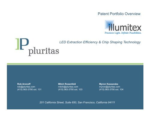
Rob Aronoff<br />
rob@pluritas.com<br />
(415) 963-3790 ext. 101<br />
Copyright ©2013 Pluritas, LLC.<br />
<strong>Patent</strong> Portfolio Overview<br />
Illumitex<br />
LED Extraction Efficiency & Chip Shaping Technology<br />
Mitch Rosenfeld<br />
mitch@pluritas.com<br />
(415) 963-3790 ext. 103<br />
Myron Kassaraba<br />
myron@pluritas.com<br />
(415) 963-3790 ext. 104<br />
201 California Street, Suite 650, San Francisco, California 94111
2<br />
Opportunity Overview<br />
Illumitex was founded in 2005 by imaging and optics industry<br />
veterans.<br />
The Company’s current business is vibrant and focused on LED total<br />
solutions including fixtures and optics. The IP being offered for <strong>sale</strong> is<br />
being divested since LED chip manufacturing is a business that is no<br />
longer being pursued.<br />
The Illumitex chip-level IP incorporates fundamental physics<br />
principles to maximize light extraction from the source. By extracting<br />
and directing photons at the die level, Illumitex delivers more usable<br />
light to the intended target while consuming less energy.<br />
This <strong>sale</strong> represents a unique opportunity for a strategic buyer to<br />
acquire lab-tested technology with very solid patent protection in a<br />
critical area of the rapidly growing LED market.<br />
Copyright ©2013 Pluritas, LLC.
3<br />
Portfolio Summary<br />
Illumitex Assets For Sale<br />
• 6 issued US patents<br />
• 1 US provisional application<br />
• 5 patent families total<br />
• Foreign equivalents from Europe, China,<br />
Japan, Taiwan, and South Korea<br />
• Forward References from:<br />
• Hon Hai Precision Industry Co.,<br />
Ltd.<br />
• Osram Opto Semiconductors<br />
• Samsung Electronics<br />
• No encumbrances<br />
Market Application and Strategic Opportunity<br />
Copyright ©2013 Pluritas, LLC.<br />
<strong>Patent</strong> Portfolio Details<br />
• US 7,789,531 (Priority: 10/2/2006)<br />
• US 7,829,358 (Priority: 2/8/2008)<br />
• US 8,087,960 (Priority: 10/2/2006)<br />
• US 8,115,217 (Priority: 12/11/2008)<br />
• US 8,217,399 (Priority: 8/1/2008)<br />
• US 8,263,993 (Priority: 2/8/2008)<br />
• US 61/587,552 (Provisional)<br />
• Foreign equivalents<br />
• The worldwide LED chips market is expected to reach $8.5 billion by 2014<br />
(http://www.marketsandmarkets.com/Market-Reports/led-chips-229.html)<br />
• Leading exemplary vendors: Nichia, Samsung, Osram, LG, Seoul Opto, Cree, Philips/Lumileds, Sharp,<br />
Toyoda Gosei, Everlight, GE, Micron, BridgeLux, SemiLEDs, Epistar, 3M, Rambus,<br />
Panasonic/Matsushita, TSMC, Rohm & Haas, Showa Denko, Toshiba, etc.<br />
(Representative market participants. Not an opinion, claim, or representation as to infringement.)
4<br />
Sorted by <strong>Patent</strong> Family (1 of 2)<br />
Pat/Pub<br />
Number<br />
Copyright ©2013 Pluritas, LLC.<br />
<strong>Patent</strong><br />
Family<br />
US 7,829,358 A<br />
US 8,263,993 A<br />
US 61/587,552<br />
(Provisional)<br />
B<br />
US 7,789,531 C<br />
US 8,087,960 C<br />
Illumitex’s IP Portfolio<br />
Tech Cluster Title<br />
LED Emitter<br />
Layer Shaping<br />
LED Emitter<br />
Layer Shaping<br />
LED Micro‐<br />
Mirrors<br />
LED Substrate<br />
Shaping (Exit<br />
Face &<br />
Sidewalls)<br />
LED Substrate<br />
Shaping (Exit<br />
Face &<br />
Sidewalls)<br />
System and method for emitter layer<br />
shaping<br />
System and method for emitter layer<br />
shaping<br />
Hybrid mirror for higher extraction<br />
efficiency from bottom‐emitting LEDs<br />
Priority<br />
Date<br />
2/8/2008<br />
2/8/2008<br />
LED system and method 10/2/2006<br />
LED system and method 10/2/2006<br />
US <strong>Patent</strong><br />
Family<br />
Members<br />
US 8,263,993<br />
(Divisional)<br />
US 7,829,358<br />
(Parent)<br />
Ex‐US<br />
<strong>Patent</strong><br />
Family<br />
Members<br />
EP2240968A1<br />
WO2009100358A1<br />
KR2010122485A<br />
CN101939849A<br />
TW200941773A<br />
JP2011512037A<br />
See ‘358 <strong>Patent</strong><br />
1/17/2012 None None<br />
US 8,087,960<br />
US20090275266A1<br />
(Abandoned)<br />
US20090275157A1<br />
(Abandoned)<br />
US 7,789,531<br />
US20090275266A1<br />
(Abandoned)<br />
US20090275157A1<br />
(Abandoned)<br />
EP2070123A2<br />
WO2009158573A1<br />
WO2009158574A1<br />
WO2008042351B1<br />
KR2009064474A<br />
CN101553928B<br />
TW201009921A<br />
TW201007993A<br />
TW200824161A<br />
JP2010506402A<br />
See ‘531 <strong>Patent</strong>
5<br />
Sorted by <strong>Patent</strong> Family (2 of 2)<br />
Pat/Pub<br />
Number<br />
Copyright ©2013 Pluritas, LLC.<br />
<strong>Patent</strong><br />
Family<br />
US 8,115,217 D LED Packaging<br />
US 8,217,399 E<br />
Illumitex’s IP Portfolio<br />
Tech Cluster Title<br />
LED Emitter &<br />
Submount<br />
Structure<br />
Photon<br />
Tunneling<br />
Systems and methods for packaging<br />
light‐emitting diode devices<br />
Photon tunneling light emitting diodes<br />
and methods<br />
Priority<br />
Date<br />
US <strong>Patent</strong><br />
Family<br />
Members<br />
12/11/2008 None<br />
8/1/2008 None<br />
Ex‐US<br />
<strong>Patent</strong><br />
Family<br />
Members<br />
WO2010068886A1<br />
TW201034256A<br />
EP2351111A1<br />
WO2010014610A1<br />
KR2011049843A<br />
CN102150285A<br />
TW201013994A<br />
JP2011530173A
6<br />
Comprehensive IP<br />
Illumitex’s IP includes proprietary technology covering different parts<br />
of an LED:<br />
<strong>Patent</strong><br />
Family D –<br />
LED<br />
Packaging:<br />
US 8,115,217<br />
Image Source:<br />
Illumitex, Fig. 4 of US 8,115,217.<br />
Copyright ©2013 Pluritas, LLC.<br />
Submount<br />
Sapphire or SiC<br />
GaN<br />
<strong>Patent</strong><br />
Family B –<br />
LED Micro-<br />
Mirrors:<br />
US Prov.<br />
61/587,552<br />
Flip-Chip LED<br />
Image Source: Illumitex.<br />
<strong>Patent</strong><br />
Family E –<br />
LED Emitter<br />
& Submount<br />
Structure<br />
Photon<br />
Tunneling:<br />
US 8,217,399<br />
<strong>Patent</strong><br />
Family C –<br />
LED<br />
Substrate<br />
Shaping (Exit<br />
Face &<br />
Sidewalls):<br />
US 7,789,531<br />
US 8,087,960<br />
<strong>Patent</strong><br />
Family A –<br />
LED Emitter<br />
Layer<br />
Shaping:<br />
US 7,829,358<br />
US 8,263,993
7<br />
Technology Overview<br />
• Light extraction from an LED chip depends on:<br />
• Minimizing the number of reflections (N) in the LED structure<br />
• Maximizing reflectivity of all surfaces<br />
• Minimizing absorption losses of all materials<br />
• Rough estimate of Losses:<br />
• Optimized structures does<br />
all of this:<br />
• Sidewall TIR:<br />
R = 100%<br />
• Sidewall shape<br />
directs light into<br />
escape cone: N = 1<br />
Copyright ©2013 Pluritas, LLC.<br />
Absorption Losses Compound!<br />
# Reflections<br />
Absorption 1<br />
R<br />
<br />
All rays strike exit<br />
face and exit!<br />
light<br />
LED<br />
Emitter<br />
Lossless<br />
reflection at<br />
sidewalls
8<br />
LED Emitter Layer Shaping<br />
US 7,829,358 & US 8,263,993<br />
LED Emitter Layer Shaping (<strong>Patent</strong> Family A)<br />
Shaped emitters achieve highest possible light extraction efficiencies<br />
(LEE)<br />
• Minimize internal reflections<br />
• Control beam shape into substrate<br />
or encapsulant<br />
Key Achievements<br />
• Light extraction improvements up to<br />
50% demonstrated<br />
• Fabrication process developed<br />
• Performance matches advanced<br />
optical modeling<br />
• Comparable test data from<br />
prototype test wafers available<br />
Copyright ©2013 Pluritas, LLC.
9<br />
LED Micro-Mirrors<br />
US Prov. 61/587,552<br />
LED Micro-Mirrors (<strong>Patent</strong> Family B)<br />
Replace conventional Ag mirror with combination of Ag & dielectric<br />
mirrors<br />
• Higher reflectivity = higher extraction<br />
efficiency<br />
Key Achievements<br />
• Dielectric stacks can give 99+% reflectance<br />
• Potential add-on process to improve conventional vertical or flipchip<br />
device designs<br />
• Demonstrated 10-15% higher extraction efficiency than PSS<br />
• Production-ready<br />
• Comparative performance data available<br />
Copyright ©2013 Pluritas, LLC.<br />
Absorption Losses Compound!<br />
# Reflections<br />
Absorption 1<br />
R<br />
Ag<br />
pCon.<br />
TiO2<br />
SiO2<br />
<br />
P‐GaN<br />
MQW‐active<br />
n‐GaN<br />
nContact
10<br />
LED Substrate Shaping<br />
(Exit Face & Sidewalls)<br />
US 7,789,531 & US 8,087,960<br />
LED Substrate Shaping (<strong>Patent</strong> Family C)<br />
Shaped substrates achieve greater<br />
efficiency than previous LEDs<br />
• The height of the substrate can be selected<br />
to limit the critical angle of rays incident<br />
on the exit surface<br />
• The exit face has at least 70% of a<br />
minimum area needed to conserve<br />
radiance for a desired half-angle of light<br />
projected from the shaped substrate<br />
Key Achievements<br />
• Theoretical efficiency of up to 89% (89% of the light entering the<br />
substrate is emitted in the desired half-angle with 11% Fresnel loss)<br />
Copyright ©2013 Pluritas, LLC.
11<br />
LED Packaging<br />
US 8,115,217<br />
LED Packaging (<strong>Patent</strong> Family D)<br />
Improved LED Packaging of <strong>Patent</strong><br />
Family C achieves overall brightness<br />
• The size of a packaged LED defines<br />
the LED’s brightness (lumens)<br />
• A phospor plate is on top or within<br />
the housing<br />
• The rays of light exit the exit face<br />
with negligible side emission<br />
through the side walls of the<br />
substrate<br />
Key Achievements<br />
• LED does not need secondary<br />
optics<br />
Copyright ©2013 Pluritas, LLC.
12<br />
LED Emitter & Submount<br />
Structure Photon Tunneling<br />
US 8,217,399<br />
Photon Tunneling (<strong>Patent</strong> Family E)<br />
Photon Tunneling increases light that makes it into air<br />
• Photons do not become trapped in the substrate<br />
• The LED layer structure has a thickness that is less than the<br />
wavelength of the light produced<br />
Key Achievements<br />
• Geometric modification<br />
of the GaN and/or<br />
substrate is not needed<br />
to extract light<br />
Copyright ©2013 Pluritas, LLC.
13<br />
Illumitex In The News<br />
Copyright ©2013 Pluritas, LLC.<br />
Sources (left to right):<br />
http://www.illumitex.com/news/news-illumitex-announces-new-ceo-and-funding/;<br />
http://ledsmagazine.com/press/33543;<br />
http://www.photonics.com/Article.aspx?AID=48616.
14<br />
Applicable Market<br />
Representative Market Participants 1<br />
1 Representative market participants. Not an opinion, claim, or representation as to infringement.<br />
Copyright ©2013 Pluritas, LLC.
15<br />
Market Trends<br />
Illumitex IP Applies to Two Large<br />
Related Growing Markets<br />
• Packaged LED Market: The worldwide packaged LED<br />
market (does not include LED chips) grew nearly 10% from<br />
$11 billion in 2010 to $12.5 billion in 2011 (the packaged<br />
LED market sorted by commercial application is shown on the<br />
immediate right)<br />
• Chip LED Market: The worldwide LED chips market was<br />
roughly $3 billion in 2009 and is estimated to grow to $8.5<br />
billion by 2014 (see lower right) – this is the applicable<br />
market for Illumitex’s IP<br />
Copyright ©2013 Pluritas, LLC.<br />
$9,000<br />
$8,000<br />
$7,000<br />
$6,000<br />
$5,000<br />
$4,000<br />
$3,000<br />
$2,000<br />
$1,000<br />
Source: LEDs Magazine, http://ledsmagazine.com/features/9/3/2 and<br />
http://www.marketsandmarkets.com/Market-Reports/led-chips-229.html<br />
$‐<br />
Worldwide Chip LED Market (in $ mil)<br />
2009 2010 2011 2012 2013 2014
16<br />
<strong>Patent</strong> Landscape Analysis<br />
The following four slides represent analysis performed on patents in<br />
the LED technology space to illustrate the relationship of the Illumitex<br />
IP to those of major market participants.<br />
Methodology<br />
• Pluritas first performed keyword and semantic searches to identify<br />
top relevant vendors within the Illumitex IP space as illustrated in<br />
Slide 17.<br />
• Pluritas then worked with IP Checkups, a research firm that<br />
provides technical analysis, to graphically map the patent<br />
landscape of top vendors by tech area as illustrated in Slide 18.<br />
• Next, by accessing IP Checkups’ LED database, Pluritas identified<br />
the vendors with “gaps” as illustrated in Slide 19 – as these<br />
companies could find this Illumitex IP useful in enhancing their<br />
patent portfolios.<br />
Copyright ©2013 Pluritas, LLC.
17<br />
<strong>Patent</strong> Landscape<br />
Leading LED Vendors 1<br />
• Pluritas performed keyword and semantic searches to identify top vendors with patents relevant to Illumitex’s IP.<br />
Using this data and collaborating with IP Checkups, the following pie chart was built illustrating the leading patent<br />
holders:<br />
Copyright ©2013 Pluritas, LLC.<br />
1 Representative market participants. Not an opinion, claim, or<br />
representation as to infringement.<br />
Efficient LED Technology: <strong>Patent</strong> Landscape (United States)<br />
Showa Denko<br />
5%<br />
Seoul Opto<br />
3%<br />
SemiLEDs<br />
1%<br />
Sharp<br />
10%<br />
Toshiba<br />
10%<br />
Samsung<br />
11%<br />
Toyoda<br />
Gosei<br />
5%<br />
Rohm & Haas<br />
4%<br />
3M Acuity<br />
1% 0%<br />
Cree<br />
6%<br />
Philips/Lumileds<br />
9%<br />
BridgeLux<br />
1%<br />
Epistar<br />
2%<br />
Panasonic<br />
11%<br />
GE<br />
2%<br />
LG<br />
8%<br />
Nichia<br />
4%<br />
Osram<br />
5%<br />
Everlight<br />
1%<br />
Goldeneye<br />
0%<br />
Source: 7,494 patents from IP Checkups’ LED Database.<br />
Illumitex<br />
3M<br />
Acuity<br />
BridgeLux<br />
Cree<br />
Epistar<br />
Everlight<br />
GE<br />
Goldeneye<br />
LG<br />
Nichia<br />
Osram<br />
Panasonic<br />
Philips/Lumileds<br />
Rohm & Haas<br />
Samsung<br />
SemiLEDs<br />
Sharp<br />
Seoul Opto<br />
Showa Denko<br />
Toshiba<br />
Toyoda Gosei
18<br />
<strong>Patent</strong> Landscape<br />
Tech Breakdown 1<br />
• The LED IP landscape for 10 Assignees is mapped by tech area below. Philips/Lumileds and LG have IP similar to the<br />
‘993, ‘358, ‘960, and ‘531 Illumitex patents. Cree, LG, and Panasonic have IP similar to the ‘217 and ‘399 Illumitex patents.<br />
<strong>Patent</strong> Family A<br />
US 8,263,993<br />
US 7,829,358<br />
Copyright ©2013 Pluritas, LLC.<br />
1 Representative market participants. Not an opinion, claim, or representation as to infringement.<br />
<strong>Patent</strong> Family C<br />
US 8,087,960<br />
US 7,789,531<br />
<strong>Patent</strong> Family D<br />
US 8,115,217<br />
Note: In the patent map, patents (dots) are clustered based on<br />
thematic similarity. Dense areas of similar patents, are represented<br />
as snow-capped peaks, while relatively sparse areas are represented<br />
as blue lakes or oceans. The absolute positioning of each peak and<br />
valley is not important, only relative location – the closer together<br />
the peaks are located on the map, the more closely the<br />
corresponding patents are related.<br />
Source: IP Checkups’ LED Database.<br />
<strong>Patent</strong> Family E<br />
US 8,217,399
19<br />
<strong>Patent</strong> Landscape<br />
Tech Breakdown 1<br />
• The table below illustrates Illumitex’s IP alongside the leading LED vendors (sorted by tech area). Cells<br />
highlighted in yellow indicate areas where vendors have fewer than 20 patents in a relevant Illumitex tech area.<br />
For example, Nichia, Sharp, Toyoda Gosei, Everlight, GE, Acuity, BridgeLux, SemiLEDs, Epistar, 3M, Goldeneye,<br />
and Rohm & Haas fewer patents than their competitors in areas relevant to the Illumitex patents.<br />
Within LED Space ‐ From IP Checkups (<strong>Patent</strong>Cam) Pats Pubs Pats Pubs Pats Pubs Pats Pubs<br />
Company US Pats US Pubs Total<br />
Illumitex 6 3 9 1 0 1 0 4 0 3 0<br />
Nichia 286 217 503 22 2 12 14 161 121 80 51<br />
Samsung 1564 1682 3246 119 76 242 191 209 312 283 398<br />
Osram 550 508 1058 124 89 34 39 176 203 58 42<br />
LG 925 499 1424 197 44 143 43 109 80 154 67<br />
Seoul Opto 158 317 475 31 28 32 34 68 151 58 103<br />
Cree 133 385 518 53 53 34 35 243 186 137 65<br />
Philips/Lumileds 975 1114 2089 156 147 49 62 292 204 179 143<br />
Sharp 810 527 1337 31 55 20 53 444 188 263 142<br />
Toyoda Gosei 335 243 578 29 19 2 8 238 160 139 87<br />
Everlight 61 89 150 24 11 15 8 5 9 7 15<br />
GE 296 235 531 52 37 13 18 58 46 34 37<br />
Acuity 4 2 6 2 1 0 0 0 0 0 0<br />
BridgeLux 73 80 153 16 20 15 14 25 18 20 10<br />
SemiLEDs 31 10 41 3 1 0 3 20 5 25 8<br />
Epistar 130 99 229 8 4 17 8 75 77 63 43<br />
3M 183 165 348 30 8 16 11 39 42 12 17<br />
Goldeneye 23 31 54 2 2 4 0 12 23 6 11<br />
Panasonic/Matsushita 970 570 1540 128 56 52 50 470 247 200 120<br />
Rohm & Haas 342 321 663 36 34 12 15 148 135 122 86<br />
Showa Denko 200 248 448 55 64 21 11 152 192 132 159<br />
Toshiba 754 619 1373 151 93 51 69 339 247 177 158<br />
Total 8809 7964 16773<br />
Copyright ©2013 Pluritas, LLC.<br />
Solid State Lighting ‐><br />
Fixtures<br />
1 Representative market participants. Not an opinion, claim, or<br />
representation as to infringement.<br />
Solid State Lighting ‐> LED<br />
Control ‐> Power<br />
Management ‐> Distribution<br />
Solid State Lighting ‐> LED<br />
Technology ‐> Chemistry &<br />
Materials ‐> Epitaxy<br />
Source: 8,809 patents and 7,964 applications from IP Checkups’ LED Database.<br />
Solid State Lighting ‐> LED<br />
Technology ‐> Chemistry &<br />
Materials ‐> Substrates
20<br />
<strong>Patent</strong> Landscape Conclusion<br />
Conclusion 1<br />
• Philips/Lumileds and LG have IP similar to Illumitex <strong>Patent</strong> Families<br />
“A” and “C”.<br />
• Cree, LG, and Panasonic have IP similar to the Illumitex <strong>Patent</strong><br />
Familities “D” and “E”.<br />
• Nichia, Sharp, Toyoda Gosei, Everlight, GE, Acuity, BridgeLux,<br />
SemiLEDs, Epistar, 3M, Goldeneye, and Rohm & Haas fewer<br />
patents than their competitors in areas relevant to the Illumitex<br />
patents.<br />
Copyright ©2013 Pluritas, LLC.<br />
1 Representative market participants. Not an opinion, claim, or<br />
representation as to infringement.
21<br />
Transaction Parameters and Objectives<br />
• Illumitex is seeking the <strong>sale</strong> of these assets<br />
• No Encumbrances<br />
• Seller requires a Grant Back license<br />
• The identity of all inquiries and bidders is confidential except as modified<br />
by a transaction between the parties<br />
Copyright ©2013 Pluritas, LLC.
22<br />
Diligence Resources Available<br />
• Technical and IP Diligence calls are available with<br />
Pluritas experts who have completed reviews of the IP<br />
assets and are knowledgeable about the markets to<br />
which they apply<br />
Copyright ©2013 Pluritas, LLC.
23<br />
For More Information<br />
• For more information and/or execution<br />
of an inquiry- and identity-protecting<br />
NDA, please contact:<br />
Rob Aronoff<br />
Managing Partner<br />
rob@pluritas.com<br />
(415) 963-3790 x101<br />
Copyright ©2013 Pluritas, LLC.<br />
Mitch Rosenfeld<br />
Partner<br />
mitch@pluritas.com<br />
(415) 963-3790 x103<br />
Myron Kassaraba<br />
Partner<br />
myron@pluritas.com<br />
(415) 963-3790 x104<br />
Craig Carothers<br />
General Counsel<br />
craig@pluritas.com<br />
(415) 963-3790 x102
24<br />
Pluritas Profile<br />
Pluritas is a transaction advisory firm specializing in divestitures,<br />
acquisitions, and mergers where Intellectual Property (IP) is a<br />
major component of the transaction.<br />
We provide arms-length sell side transaction services to all<br />
owners of IP assets. We provide arms-length buy side<br />
transaction services to a select group of Corporate Clients.<br />
We expertly navigate the risks and nuances for all parties<br />
involved with transacting IP, yielding a 'safer' and more<br />
comfortable transaction climate for all participants.<br />
We also strongly differentiate ourselves by our track record<br />
of success, as well as by integrating seasoned professionals<br />
with deep industry, technical and IP expertise into every<br />
engagement.<br />
Copyright ©2013 Pluritas, LLC.
25<br />
NOTICE<br />
THIS PRESENTATION DOES NOT CONSTITUTE AN OFFER FOR SALE OF<br />
ASSETS OR SECURITIES FOR ILLUMITEX OR AN OFFER FOR, OR<br />
SOLICITATION OF, A LICENSE OF ANY KIND. IN MAKING A DECISION<br />
REGARDING THE ILLUMITEX OPPORTUNITY, POTENTIAL PURCHASERS<br />
MUST RELY ON THEIR OWN EXAMINATION OF THE INTELLECTUAL<br />
PROPERTY RIGHTS AND OTHER ASSETS INCLUDING BUT NOT LIMITED TO<br />
THE TITLE, VALUE, MERITS AND RISKS INVOLVED. THERE IS NO<br />
ASSURANCE THAT THESE INTELLECTUAL PROPERTY RIGHTS WILL BE<br />
UPHELD. PLURITAS MAKES NO REPRESENTATION CONCERNING THE<br />
VALIDITY OF THE INTELLECTUAL PROPERTY HEREIN. ADDITIONALLY,<br />
THESE MATERIALS ARE SOLELY ATTRIBUTABLE TO PLURITAS AND DO<br />
NOT NECESSARILY REPRESENT THE VIEWS OR OPINIONS OF ILLUMITEX.<br />
NOTHING IN THIS DOCUMENT SHALL CONSTITUTE OR BE INTERPRETED AS<br />
LEGAL ANALYSIS REGARDING THE SCOPE OF THE PATENTS OR OTHER<br />
INTELLECTUAL PROPERTY RIGHTS. SIMILARLY, NOTHING INCLUDED IN<br />
THIS DOCUMENT SHALL BE USED TO INTERPRET, DEFINE, OR OTHERWISE<br />
LIMIT THE SCOPE AFFORDED THE ASSOCIATED INTELLECTUAL PROPERTY<br />
RIGHTS.<br />
Copyright ©2013 Pluritas, LLC.
26<br />
Copyright ©2013 Pluritas, LLC.<br />
Appendix: Exemplary Claims
27<br />
U.S. <strong>Patent</strong> No. 7,789,531 – Representative Claim<br />
‘531 <strong>Patent</strong>, Claim 1<br />
Copyright ©2013 Pluritas, LLC.<br />
Representative Claim<br />
An LED comprising:<br />
a quantum well region operable to generate light; and<br />
a shaped substrate having an interface to receive light generated by the quantum well region,<br />
wherein light generated by the quantum well region traverses the interface, the shaped<br />
substrate comprising:<br />
an exit face opposite from and a distance from the interface, wherein the substrate is<br />
shaped so that a portion of the light entering the shaped substrate through the interface will<br />
exit the shaped substrate through the exit face and wherein the exit face has at least 70% of<br />
a minimum area necessary to conserve radiance for a desired half-angle of light projected<br />
from the shaped substrate; and<br />
a set of sidewalls, wherein each sidewall is positioned and shaped so that at least a<br />
majority of rays having a straight transmission path from the interface to that sidewall can<br />
reflect through total internal reflection to the exit face with an angle of incidence at the exit<br />
face at less than or equal to a critical angle at the exit face.
28<br />
U.S. <strong>Patent</strong> No. 7,829,358 – Representative Claim<br />
’358 <strong>Patent</strong>, Claim 1<br />
Copyright ©2013 Pluritas, LLC.<br />
Representative Claim<br />
A method of shaping an emitter layer of the LED, comprising:<br />
determining an exit area (b) and an emitter area (a) of a miniature emitter, wherein the exit<br />
area (b) has an exit face in a first geometric configuration and wherein the emitter area (a)<br />
has a quantum well region in a second geometric configuration;<br />
determining a minimum height (h) of the miniature emitter utilizing the exit area (b) and the<br />
emitter area (a);<br />
removing matter from an emitting material or growing the emitting material according to the<br />
first geometric configuration, the second geometric configuration, and the minimum height (h)<br />
to form a shaped portion having one or more miniature emitters meeting the minimum height<br />
(h); and<br />
shaping sidewalls of the miniature emitters, wherein each sidewall is positioned and shaped to<br />
cause at least a majority of rays having a straight transmission path from the emitter area to<br />
that sidewall to reflect to the exit face with an angle of incidence at the exit face at less than<br />
or equal to a critical angle at the exit face.
29<br />
U.S. <strong>Patent</strong> No. 8,087,960 – Representative Claim<br />
’960 <strong>Patent</strong>, Claim 11<br />
Copyright ©2013 Pluritas, LLC.<br />
Representative Claim<br />
A method of shaping an LED comprising:<br />
providing a wafer comprising a substrate and one or more layers for a quantum well region of the LED;<br />
grinding the substrate to form a shaped substrate portion of the LED;<br />
wherein the shaped substrate portion is shaped to comprise:<br />
an exit face opposite from and a distance from an interface with the to receive light generated by a quantum well<br />
region of the LED, the exit face having a size being at least 70% of a minimum area necessary to conserve radiance<br />
for a desired half-angle of light projected from the shaped substrate; and<br />
a set of sidewalls, wherein each sidewall is positioned and shaped so that at least a majority of rays having a<br />
straight transmission path from the interface to that sidewall reflect through total internal reflection to the exit face<br />
with an angle of incidence at the exit face of less than or equal to a critical angle at the exit face; wherein the method<br />
is performed by performing steps in the order of:<br />
(a) determining boundary conditions for the shaped substrate portion of the LED, wherein the boundary conditions<br />
comprise the size of the exit face of the shaped substrate portion of the LED and the distance between the exit face<br />
and the interface between the shaped substrate portion and the quantum well region of the LED;<br />
(b) determining the shapes and positions of the set of sidewalls of the shaped substrate portion of the LED; and<br />
(c) shaping the shaped substrate portion of the LED.
30<br />
U.S. <strong>Patent</strong> No. 8,115,217 – Representative Claim<br />
‘217 <strong>Patent</strong>, Claim 1<br />
Copyright ©2013 Pluritas, LLC.<br />
Representative Claim<br />
A packaged light-emitting diode (LED) device, comprising:<br />
a housing having a cavity;<br />
a phosphor plate on top or within the housing;<br />
a submount attached to the housing, wherein the submount comprises metal traces,<br />
vias, or a combination thereof; and<br />
at least one LED chip residing in the cavity of the housing between the phosphor plate<br />
and the submount and comprising a substrate and a light emitting region, wherein the<br />
substrate comprises a side wall and an exit face on top of the side wall, wherein all or<br />
substantially all rays of light emitting from the light emitting region exit the exit face with<br />
negligible or substantially negligible side emission through the side wall of the<br />
substrate, and wherein the light emitting region is connected to the metal traces of the<br />
submount inside the housing through an electrically conductive contact area.
31<br />
U.S. <strong>Patent</strong> No. 8,217,399 – Representative Claim<br />
’399 <strong>Patent</strong>, Claim 1<br />
Copyright ©2013 Pluritas, LLC.<br />
Representative Claim<br />
A light-emitting diode (LED) device comprising:<br />
an LED layer structure comprising a quantum well layer adapted to generate light having<br />
a wavelength, a p-doped alloy layer on a first side of the quantum well layer, an ndoped<br />
alloy layer on a second side of the quantum well layer obverse from the first side<br />
and between the quantum well layer and a medium;<br />
an electrode electrically connected to the p-doped alloy layer; and<br />
an electrode electrically connected to the n-doped alloy layer;<br />
wherein the combined thickness of the LED layer structure on the second side of the<br />
quantum well layer including the n-doped alloy layer is thinner than the wavelength of<br />
light that the quantum well layer is adapted to generate to allow light generated by the<br />
quantum well layer to photon tunnel to the medium.
32<br />
U.S. <strong>Patent</strong> No. 8,263,993 – Representative Claim<br />
’993 <strong>Patent</strong>, Claim 1<br />
Copyright ©2013 Pluritas, LLC.<br />
Representative Claim<br />
An LED, comprising:<br />
a base substrate; and<br />
an emitter layer on a surface of the substrate configured to emit light in an emission half angle,<br />
wherein the emitter layer has a shaped portion comprising:<br />
an emitter area;<br />
an exit area a height from the emitter area;<br />
sidewalls running from the emitter area to the exit area, wherein each of the sidewalls comprises<br />
a plurality of areas at different angles relative to the emitter area and wherein each sidewall is<br />
positioned and shaped to cause at least a majority of rays having a straight transmission path from<br />
the emitter area to that sidewall to reflect to the exit area with an angle of incidence at the exit area<br />
at less than or equal to a critical angle at an emitter layer to substrate boundary; and<br />
wherein the size of the exit area and shapes of the sidewalls are configured so that at least 60%<br />
of the light generated in the emitter layer exits the emitter layer into the substrate in the emission<br />
half angle.