conducters by Impact of EMP and UWB Pulses
conducters by Impact of EMP and UWB Pulses
conducters by Impact of EMP and UWB Pulses

Create successful ePaper yourself
Turn your PDF publications into a flip-book with our unique Google optimized e-Paper software.
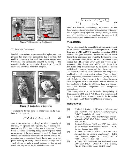
a)<br />
Figure 17. Destruction <strong>of</strong> Onchipwires<br />
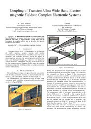
V.3 Bondwire Destructions<br />
Bondwire destructions always occured at higher pulse amplitudes<br />
than onchipwire destructions due to the fact, that<br />
onchipwires normaly has much lower cross sections than<br />
bondwires. The destructions occured <strong>by</strong> melting <strong>of</strong> the<br />
material similar to onchipwire destructions. Figure 18<br />
shows two destructed bondwires <strong>and</strong> pads.<br />
a) b)<br />
Figure 18. Destructions <strong>of</strong> Bondwires<br />
The energy to destruct bond- or onchipwires can be calculated<br />
via the equation [5]<br />
( melt sur ) T T c l A Q − ⋅ ⋅ ⋅ ⋅ = ρ<br />
with A = cross section, l = length <strong>of</strong> wire, ρ = density <strong>of</strong><br />
material, c = specific heat capacity, Tmelt = melting temperature<br />
<strong>and</strong> Tsur = surrounding area temperature. Equation<br />
1 shows that the melting energy strictly depends on the<br />
cross section, if the same material is used for bond- <strong>and</strong><br />
onchipwires under the constraint heat transfer into the surrounding<br />
area is neglectable (valid due to short pulse impact).<br />
Drawing an energy balance results in equation 2<br />
which allows to make a rough estimate <strong>of</strong> the current<br />
which was responsible for the bondwire destruction.<br />
b)<br />
(1)<br />
I =<br />
With κ = electrical conductivity, d = diameter <strong>of</strong> the<br />
bondwires <strong>and</strong> the assumption that the duration <strong>of</strong> the current<br />
is approximately equivalent to the pulse length, a current<br />
<strong>of</strong> I ≈ 400 A can be calculated via equation 2 if<br />
bondwires made <strong>of</strong> aluminium were implemented.<br />
VI. SUMMARY<br />
The investigation <strong>of</strong> the susceptibility <strong>of</strong> logic devices built<br />
in ten different semiconductor technologies (NANDs <strong>and</strong><br />
Inverter) to <strong>EMP</strong> <strong>and</strong> <strong>UWB</strong> pulses has shown, that CMOS<br />
devices first gets reversible breakdowns <strong>and</strong> at much<br />
higher field amplitudes non reversible destructions occur.<br />
The destruction thresholds <strong>of</strong> TTL <strong>and</strong> CMOS devices are<br />
similar but TTL devices always gets non reversible destructions.<br />
The breakdown- (BT) <strong>and</strong> destructionthresholds<br />
(DT) decreases much <strong>by</strong> extending the ribbon<br />
cable length or usage <strong>of</strong> pulses with faster rise times.<br />
The destruction effects can be separated into componentonchipwire-<br />
<strong>and</strong> bondwire-destructions. First, at lower<br />
field amplitudes, component destructions ,mostly as a result<br />
<strong>of</strong> flashover effects, occur. If the amplitude increases<br />
also onchipwire destructions appear. Further increase <strong>of</strong><br />
the amplitude is leading to additional bondwire destructions<br />
<strong>and</strong> multiple component- <strong>and</strong> onchipwiredestructions.<br />
This investigation is part <strong>of</strong> the study “Susceptibility <strong>of</strong><br />
Electronics to <strong>EMP</strong> <strong>and</strong> <strong>UWB</strong>, Phase II”, commissioned<br />
<strong>by</strong> the Armed Forces Scientific Institute for Protection<br />
Technologies - ABC-Protection (Munster, Germany).<br />
REFERENCES<br />
2 4<br />
ρ ⋅κ<br />
⋅c<br />
⋅π<br />
⋅d<br />
⋅(<br />
T<br />
16⋅<br />
∆t<br />
melt<br />
−T<br />
[1] D.Nitsch, J.Schlüter, H.J.Kitschke, “Generierung<br />
und Vorteile von Ultrawideb<strong>and</strong>-Impulsen”,<br />
EMV99, Mannheim, Germany<br />
[2] C.Braun, “Aufbau eines breitb<strong>and</strong>igen Wellenleiters<br />
für N<strong>EMP</strong> Modell Simulationen”, INT Bericht<br />
Okt. 84<br />
[3] D.Nitsch, M.Camp, "<strong>UWB</strong> <strong>and</strong> <strong>EMP</strong> Susceptibility<br />
<strong>of</strong> Modern Microprocessorboards", EMC<br />
Europe, Brugge, Sept. 2000<br />
[4] M.Camp, H.Garbe, D.Nitsch, "<strong>UWB</strong> <strong>and</strong> <strong>EMP</strong><br />
Susceptibility <strong>of</strong> Modern Electronics", IEEE<br />
EMC, Montreal, August 13-17, 2001, ISBN: 0-<br />
7803-6569-0, pp. 1015-1020<br />
[5] M.Camp, “Empfindlichkeit von Elektronik gegen<br />
<strong>EMP</strong> und <strong>UWB</strong> - Phase II”, WIS Bericht,<br />
Okt. 01, AN:005.H-0 A064, AG:UT 243-C<br />
sur<br />
)<br />
(2)