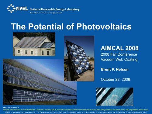
The Potential of Photovoltaics (Presentation)
The Potential of Photovoltaics (Presentation)
The Potential of Photovoltaics (Presentation)

You also want an ePaper? Increase the reach of your titles
YUMPU automatically turns print PDFs into web optimized ePapers that Google loves.
<strong>The</strong> <strong>Potential</strong> <strong>of</strong> <strong>Photovoltaics</strong><br />
AIMCAL 2008<br />
2008 Fall Conference<br />
Vacuum Web Coating<br />
Brent P. Nelson<br />
October 22, 2008<br />
NREL/PR-520-44106<br />
Presented at the Association <strong>of</strong> Industrial Metallizers, Coaters and Laminators (AIMCAL) Fall Technical Conference 2008 and 22nd International Vacuum Web Coating Conference held October 19-22, 2008 in Myrtle Beach, South Carolina.<br />
NREL is a national laboratory <strong>of</strong> the U.S. Department <strong>of</strong> Energy Office <strong>of</strong> Energy Efficiency and Renewable Energy operated by the Alliance for Sustainable Energy, LLC
<strong>The</strong> <strong>Potential</strong> <strong>of</strong> PV: Course Outline<br />
1. <strong>The</strong> Energy Market<br />
2. Introduction to <strong>Photovoltaics</strong> (PV)<br />
3. Current PV Technologies<br />
a) crystalline silicon (c-Si)<br />
b) amorphous silicon (a-Si:H)<br />
c) cadmium telluride (CdTe)<br />
d) copper indium gallium selenide (CIGS)<br />
e) others, concentrator PV, organic PV, sensitized cells, etc.<br />
4. Technology Comparison<br />
5. PV Technology Trajectory<br />
National Renewable Energy Laboratory Innovation for Our Energy Future
Breakdown <strong>of</strong> US Energy Use<br />
National Renewable Energy Laboratory Innovation for Our Energy Future
We use Mostly Chemical Energy<br />
National Renewable Energy Laboratory Innovation for Our Energy Future
World’s Consumable Resources<br />
Breeder Reactors<br />
“Conventional” “Future”<br />
Quads BBoO<br />
29,890<br />
23,912<br />
17,934<br />
11,956<br />
5,978<br />
0<br />
5,153<br />
4,122<br />
3,092<br />
2,061<br />
1,031<br />
0
Sustainable Resource <strong>Potential</strong><br />
TW<br />
40<br />
30<br />
20<br />
10<br />
0<br />
Oceans<br />
Resource Limit<br />
Practical <strong>Potential</strong><br />
Hydro<br />
Biomass<br />
Geothermal<br />
70 TW > 100 TW<br />
Wind<br />
Solar
Consumable Resources<br />
“Conventional” “Future”<br />
Hours<br />
80<br />
64<br />
48<br />
32<br />
16<br />
0<br />
What are these units <strong>of</strong> time<br />
<strong>of</strong> sunlight hitting the earth?
Concentrating<br />
Solar Power<br />
Solar Energy Technologies<br />
Solar<br />
Hot Water<br />
Passive Solar<br />
(space heating)<br />
Solar Electric - <strong>Photovoltaics</strong>
<strong>The</strong> Basic Solar Cell<br />
National Renewable Energy Laboratory Innovation for Our Energy Future
PV Systems Building Blocks<br />
Cell<br />
Module<br />
Array<br />
System<br />
Includes storage,<br />
voltage regulation,<br />
inverters, etc.<br />
National Renewable Energy Laboratory Innovation for Our Energy Future
PV Technologies<br />
Flat plates<br />
Concentrators<br />
Generation<br />
Crystalline silicon<br />
1<br />
Thin films<br />
2<br />
New technologies<br />
3<br />
Silicon<br />
1<br />
2<br />
Multijunctions<br />
(III-Vs)
2007 Flat Plate Module Production<br />
Source: Paul Maycock, PV News, February 2005<br />
Generation<br />
1<br />
2<br />
Thin-Films<br />
3,733 MW Total Production<br />
• 90% is crystalline silicon<br />
• 10% is thin-films (pulled out)<br />
• 95% contains silicon (greens)
Crystalline Silicon = Wafers<br />
Single Crystal Si<br />
Multicrystalline Si<br />
Wafering<br />
Ribbons ≠ Wafering<br />
String Ribbon Si<br />
Edge-Defined<br />
Film-Fed Growth<br />
(EFG) Si
c-Si – Device Structure<br />
Best Commercial<br />
Sample Structure<br />
Point-contact cell<br />
SunPower – 21.5%<br />
Common Industrial<br />
Cell Structure<br />
AR coating<br />
N type diffusion<br />
P type wafer<br />
Back contact<br />
Front Contact
C-Si Modules
Crystalline Silicon (c-Si)<br />
Pros<br />
•Well understood material system<br />
because <strong>of</strong> IC industry<br />
•Equipment to production is<br />
readily available from multiple<br />
vendors.<br />
•Lower barriers to entry for new<br />
companies<br />
•Elemental abundance<br />
Cons<br />
•Si wafers are energy intensive<br />
to manufacture<br />
•Feed stock processing growth<br />
rate constrains growth<br />
•Actually a family <strong>of</strong> several<br />
device structures, substrates,<br />
and production technologies<br />
•Indirect band gap<br />
•Not monolithically processed<br />
•Wafer technology<br />
(too thick ~ 200 microns)<br />
•Not many web-coating<br />
applications
Amorphous Silicon: Very Thin<br />
a-Si:H<br />
B or P dopants<br />
can be fully satisfied<br />
∴ need %-levels<br />
hν<br />
Transparent Top Contact<br />
p-layer<br />
i-layer<br />
n-layer<br />
Back Reflecting Metal
Typical Growth Techniques<br />
• Encapsulation<br />
• Laser Patterning<br />
• Top Contacts<br />
– Metal Grids…<br />
fingers by PVD or wire<br />
– TCO’s… ZnO, ITO by PVD<br />
• Semiconductor Layers<br />
– CVD techniques<br />
– PVD in research<br />
• Bottom Contacts<br />
– Metals… Ag, Al, by PVD<br />
– Texturing… ZnO by PVD<br />
Growth Direction<br />
Transparent Top Contact<br />
p-layer<br />
i-layer<br />
n-layer<br />
Back Reflecting Metal
a-Si:H Modules
Amorphous Silicon (a-Si:H)<br />
Pros<br />
•Well understood material system<br />
– lots <strong>of</strong> science<br />
•Leverage <strong>of</strong>f TFT industry<br />
•At least three companies selling<br />
“turn key manufacturing” facilities<br />
•Elemental abundance<br />
•Scalable manufacturing<br />
techniques<br />
•Low temperature processes<br />
•Very thin absorbers<br />
•Many web-coating applications<br />
Cons<br />
•Doesn’t work well in red end <strong>of</strong><br />
solar spectrum<br />
•Low hole-mobility<br />
•Light induced metastability<br />
•Lowest efficiency <strong>of</strong> readily<br />
available technologies<br />
•Many size “standards”<br />
•Many substrate “standards”
Cell Thickness (μm)<br />
Future <strong>of</strong> Film-Silicon PV<br />
100<br />
10<br />
1<br />
a-Si:H<br />
< 300°C<br />
nc-Si:H<br />
< 300°C<br />
pc-Si<br />
CVD<br />
~1000°C<br />
pc-Si<br />
pc-Si, MIC,<br />
LTE, < 300°C<br />
APIVT<br />
mc-Si<br />
epi, ZMR<br />
APIVT<br />
> 1000°C<br />
0.1 1.0 10 100 1,000<br />
Grain Size (μm)<br />
1410°C<br />
Wafers<br />
c-Si<br />
epi, lift,<br />
smart cut<br />
> 1000°C<br />
< 800°C
CdTe – Device Structure<br />
Best Laboratory<br />
sample structure<br />
GRAIN BOUNDARY<br />
8-10 µ<br />
~1 µ<br />
Common Industrial<br />
module structure<br />
C-Paste with Cu<br />
Or metals<br />
CdTe 1.5-4 µm<br />
CdS 600-2000Ǻ<br />
SnO2 .2-.5 µm<br />
Glass<br />
Process<br />
Direction<br />
Ref: Tim Gessert, 3M Tech Forum, 7/19/06
“Typical” CdTe Process<br />
Ref: G. Braun & D. Skinner, Experience Scaling-Up Manufacturing <strong>of</strong> Emerging Photovolltaic<br />
Technologies, NREL SR-640-39165, Jan 2007, p 42
CdTe Modules
CdTe – Thin film<br />
Pros<br />
•Low Manufacturing Cost<br />
•Highest deposition rate <strong>of</strong><br />
absorber materials = good<br />
Manufacturability<br />
•High efficiency laboratory cells<br />
= great promise<br />
•Best Laboratory: > 16%<br />
•Champion Modules at 12.5%<br />
•Monolithic Module construction<br />
•Nice Aesthetics<br />
•2 component manufacturing<br />
that is very impurity tolerant<br />
Cons<br />
•Not as well understood as Si<br />
materials<br />
•No Industry standard size or<br />
fabrication techniques<br />
•No one sells equipment to<br />
build these modules.<br />
•Commercial Modules: 8-10.5<br />
•Cd toxicity issues are know,<br />
and CdTe toxicity issues are<br />
being debated.<br />
•Not currently many webcoating<br />
applications
CIGS – Device Structure<br />
Process<br />
Direction<br />
Ref: Tim Gessert, 3M Tech Forum, 7/19/06<br />
• Zn - Zinc<br />
• O - Oxygen<br />
• Sn - Tin<br />
• Cd – Cadmium<br />
• S – Sulphur<br />
• Cu - Copper<br />
• In - Indium<br />
• Ga - Gallium<br />
• Se – Selenium<br />
• Mo - Molybdenum
“Typical” CIGS Process<br />
Co Evaporate<br />
CuGaInSe 2<br />
CBD <strong>of</strong> CdS<br />
Sputter<br />
undoped ZnO<br />
Sputter<br />
Al-doped ZnO<br />
Research Standard<br />
Sputter Mo<br />
Sputter Cu<br />
Sputter InGa<br />
Reactive anneal<br />
In H 2Se, S, vapor<br />
Sputter CdS<br />
Sputter ITO<br />
Manufacturing Example<br />
Can also be:<br />
•Electrodepositon<br />
•<strong>The</strong>rmal evaporation<br />
•Electron beam evaporation<br />
•Screen printing<br />
•Spray jet<br />
Can also be:<br />
Annealed with vapor <strong>of</strong><br />
•H 2S<br />
•Se<br />
•S<br />
Can also be:<br />
•ZnO, ZnS, ZnSe,<br />
•InS, ZnIn xSe y<br />
•In x(OH,S) y<br />
•In 2S 3<br />
Ref: Handbook <strong>of</strong> Photovoltaic Science and Engineering, Luque and Hegedus,<br />
chapter 13, Shafaman and Stolt, p 583.
CIGS Modules
CIGS – Thin film<br />
Pros<br />
•Possible low manufacturing cost<br />
•Possible high deposition rate <strong>of</strong><br />
absorber materials<br />
•Highest efficiency laboratory cells<br />
= great promise<br />
•Best Laboratory: > 19.9%<br />
•Monolithic Module construction<br />
•Very Nice Aesthetics<br />
•Three “turn-key factory”<br />
companies<br />
•Many web-coating applications<br />
Cons<br />
•Requires large area<br />
stoichiometry <strong>of</strong> 4 elements<br />
•High efficiency processes<br />
require strict uniformity<br />
•Not as well understood as Si<br />
materials<br />
•No Industry standard for size or<br />
fabrication techniques<br />
•Best Commercial Modules:<br />
13.4%<br />
•Increasing deposition rates<br />
lowers efficiency
Concentrator <strong>Photovoltaics</strong> (CPV)<br />
• Flat plate collectors<br />
• cover large areas with low cost cells<br />
• don’t require external optics<br />
• Concentrator<br />
• high efficiency cells<br />
• cover large areas with low cost external optics<br />
• Mid to high-concentration PV systems<br />
• high-efficiency III-V or Si cells<br />
• trackers<br />
• reflective optics or<br />
• refractive optics<br />
• CPV is inherently system-oriented<br />
• CPV requires direct sun (SW USA)<br />
National Renewable Energy Laboratory Innovation for Our Energy Future
Exciton-Based Materials<br />
Traditional<br />
Semiconductor<br />
Charge<br />
Separation<br />
at Interface<br />
Conducting<br />
Polymer<br />
National Renewable Energy Laboratory Innovation for Our Energy Future
Organic Solar Cells<br />
National Renewable Energy Laboratory Innovation for Our Energy Future
Grätzel (Dye-Sensitized) Cells<br />
High surface area<br />
for rutheniumpolypyridine<br />
dye<br />
National Renewable Energy Laboratory Innovation for Our Energy Future<br />
Ox<br />
Red
All PV Technologies are Improving<br />
National Renewable Energy Laboratory Innovation for Our Energy Future
Flat Panel PV Modules & Cells<br />
From Citigroup Global Markets, equity research,<br />
Applied Materials, Inc, (AMT), 19 Feb. 2008<br />
National Renewable Energy Laboratory Innovation for Our Energy Future
Worldwide PV Module Production<br />
Thin-Films<br />
National Renewable Energy Laboratory Innovation for Our Energy Future
Thin-Film Market Share in the USA<br />
National Renewable Energy Laboratory Innovation for Our Energy Future
Conclusions<br />
1. <strong>The</strong> sun is the BIG energy player<br />
2. PV can (should) be a big part <strong>of</strong> the Energy Portfolio<br />
3. Some PV types have web-coating applications<br />
a) crystalline silicon (c-Si) - LOW<br />
b) amorphous silicon (a-Si:H) - VERY HIGH<br />
c) cadmium telluride (CdTe) - POTENTIAL<br />
d) copper indium gallium selenide (CIGS) - HIGH<br />
e) others (CPV, OPV, DSSC, etc.) – VERY HIGH<br />
4. PV industry is “a mile wide and an inch deep”<br />
5. PV production growing a 35%++ annually<br />
National Renewable Energy Laboratory Innovation for Our Energy Future<br />
but still very small