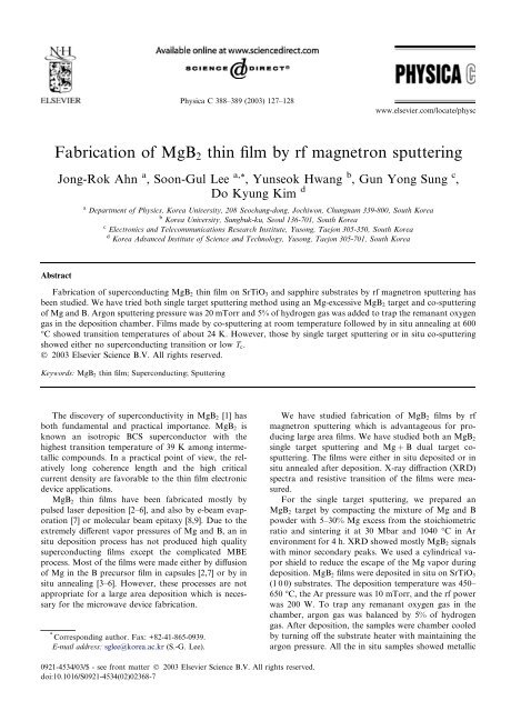
Fabrication of MgB2 thin film by rf magnetron sputtering
Fabrication of MgB2 thin film by rf magnetron sputtering
Fabrication of MgB2 thin film by rf magnetron sputtering

Create successful ePaper yourself
Turn your PDF publications into a flip-book with our unique Google optimized e-Paper software.
<strong>Fabrication</strong> <strong>of</strong> <strong>MgB2</strong> <strong>thin</strong> <strong>film</strong> <strong>by</strong> <strong>rf</strong> <strong>magnetron</strong> <strong>sputtering</strong><br />
Abstract<br />
Jong-Rok Ahn a , Soon-Gul Lee a,* , Yunseok Hwang b , Gun Yong Sung c ,<br />
Do Kyung Kim d<br />
a Department <strong>of</strong> Physics, Korea University, 208 Seochang-dong, Jochiwon, Chungnam 339-800, South Korea<br />
b Korea University, Sungbuk-ku, Seoul 136-701, South Korea<br />
c Electronics and Telecommunications Research Institute, Yusong, Taejon 305-350, South Korea<br />
d Korea Advanced Institute <strong>of</strong> Science and Technology, Yusong, Taejon 305-701, South Korea<br />
<strong>Fabrication</strong> <strong>of</strong> superconducting <strong>MgB2</strong> <strong>thin</strong> <strong>film</strong> on SrTiO3 and sapphire substrates <strong>by</strong> <strong>rf</strong> <strong>magnetron</strong> <strong>sputtering</strong> has<br />
been studied. We have tried both single target <strong>sputtering</strong> method using an Mg-excessive <strong>MgB2</strong> target and co-<strong>sputtering</strong><br />
<strong>of</strong> Mg and B. Argon <strong>sputtering</strong> pressure was 20 mTorr and 5% <strong>of</strong> hydrogen gas was added to trap the remanant oxygen<br />
gas in the deposition chamber. Films made <strong>by</strong> co-<strong>sputtering</strong> at room temperature followed <strong>by</strong> in situ annealing at 600<br />
°C showed transition temperatures <strong>of</strong> about 24 K. However, those <strong>by</strong> single target <strong>sputtering</strong> or in situ co-<strong>sputtering</strong><br />
showed either no superconducting transition or low Tc.<br />
Ó 2003 Elsevier Science B.V. All rights reserved.<br />
Keywords: <strong>MgB2</strong> <strong>thin</strong> <strong>film</strong>; Superconducting; Sputtering<br />
The discovery <strong>of</strong> superconductivity in <strong>MgB2</strong> [1] has<br />
both fundamental and practical importance. <strong>MgB2</strong> is<br />
known an isotropic BCS superconductor with the<br />
highest transition temperature <strong>of</strong> 39 K among intermetallic<br />
compounds. In a practical point <strong>of</strong> view, the relatively<br />
long coherence length and the high critical<br />
current density are favorable to the <strong>thin</strong> <strong>film</strong> electronic<br />
device applications.<br />
<strong>MgB2</strong> <strong>thin</strong> <strong>film</strong>s have been fabricated mostly <strong>by</strong><br />
pulsed laser deposition [2–6], and also <strong>by</strong> e-beam evaporation<br />
[7] or molecular beam epitaxy [8,9]. Due to the<br />
extremely different vapor pressures <strong>of</strong> Mg and B, an in<br />
situ deposition process has not produced high quality<br />
superconducting <strong>film</strong>s except the complicated MBE<br />
process. Most <strong>of</strong> the <strong>film</strong>s were made either <strong>by</strong> diffusion<br />
<strong>of</strong> Mg in the B precursor <strong>film</strong> in capsules [2,7] or <strong>by</strong> in<br />
situ annealing [3–6]. However, these processes are not<br />
appropriate for a large area deposition which is necessary<br />
for the microwave device fabrication.<br />
* Corresponding author. Fax: +82-41-865-0939.<br />
E-mail address: sglee@korea.ac.kr (S.-G. Lee).<br />
Physica C 388–389 (2003) 127–128<br />
0921-4534/03/$ - see front matter Ó 2003 Elsevier Science B.V. All rights reserved.<br />
doi:10.1016/S0921-4534(02)02368-7<br />
www.elsevier.com/locate/physc<br />
We have studied fabrication <strong>of</strong> <strong>MgB2</strong> <strong>film</strong>s <strong>by</strong> <strong>rf</strong><br />
<strong>magnetron</strong> <strong>sputtering</strong> which is advantageous for producing<br />
large area <strong>film</strong>s. We have studied both an <strong>MgB2</strong><br />
single target <strong>sputtering</strong> and Mg þ B dual target co<strong>sputtering</strong>.<br />
The <strong>film</strong>s were either in situ deposited or in<br />
situ annealed after deposition. X-ray diffraction (XRD)<br />
spectra and resistive transition <strong>of</strong> the <strong>film</strong>s were measured.<br />
For the single target <strong>sputtering</strong>, we prepared an<br />
<strong>MgB2</strong> target <strong>by</strong> compacting the mixture <strong>of</strong> Mg and B<br />
powder with 5–30% Mg excess from the stoichiometric<br />
ratio and sintering it at 30 Mbar and 1040 °C inAr<br />
environment for 4 h. XRD showed mostly <strong>MgB2</strong> signals<br />
with minor secondary peaks. We used a cylindrical vapor<br />
shield to reduce the escape <strong>of</strong> the Mg vapor during<br />
deposition. <strong>MgB2</strong> <strong>film</strong>s were deposited in situ on SrTiO3<br />
(1 0 0) substrates. The deposition temperature was 450–<br />
650 °C, the Ar pressure was 10 mTorr, and the <strong>rf</strong> power<br />
was 200 W. To trap any remanant oxygen gas in the<br />
chamber, argon gas was balanced <strong>by</strong> 5% <strong>of</strong> hydrogen<br />
gas. After deposition, the samples were chamber cooled<br />
<strong>by</strong> turning <strong>of</strong>f the substrate heater with maintaining the<br />
argon pressure. All the in situ samples showed metallic
128 J.-R. Ahn et al. / Physica C 388–389 (2003) 127–128<br />
behavior in the resistance versus temperature (R–T )<br />
measurements. Although a few <strong>of</strong> them showed resistance<br />
anomalies at 30–40 K, they did not show a distinct<br />
superconducting transition. In XRD spectra <strong>MgB2</strong> signals<br />
were not identified. We also made <strong>film</strong>s without the<br />
vapor shield. The <strong>film</strong> deposition rate was lower compared<br />
with the shielded case. In addition, the R–T curve<br />
was semiconducting or barely metallic at best. In the<br />
single target <strong>sputtering</strong> study, it is believed that the<br />
stoichiometric <strong>MgB2</strong> phase was difficult to achieve due<br />
to the extreme disparity <strong>of</strong> vapor pressure between Mg<br />
and B <strong>sputtering</strong>, and the relatively slow deposition rate.<br />
Co-<strong>sputtering</strong> <strong>by</strong> using Mg and B targets was much<br />
more advantageous in terms <strong>of</strong> the <strong>film</strong> stoichiometry.<br />
Since the ratio <strong>of</strong> the molar densities <strong>of</strong> Mg (0.0716 mol/<br />
cm 3 ) and B (0.217 mol/cm 3 ) is 1:3, the deposition ratio<br />
(thickness/unit time) <strong>of</strong> Mg : B ¼ 3 : 2 will guarantee the<br />
<strong>MgB2</strong> stoichiometry. However, to compensate the loss<br />
<strong>of</strong> Mg during the in situ annealing, the deposition rate <strong>of</strong><br />
Mg was adjusted at higher values than the stoichiometric<br />
ratio. <strong>rf</strong> power used was 250 W for B target and<br />
70 W for Mg target. The deposition rates at those<br />
powers were 9 nm/min for B and 20 nm/min for Mg.<br />
Films were made <strong>by</strong> co-deposition <strong>of</strong> Mg and B on<br />
Al2O3(1 1 0 2) substrates at 20 mTorr <strong>of</strong> Ar at room<br />
temperature for 30 min, followed <strong>by</strong> in situ annealing.<br />
After deposition the <strong>film</strong> was heated to 600 °C at the rate<br />
<strong>of</strong> 60 °C/min, annealed at 600 °C for 20 min, and finally<br />
cooled down <strong>by</strong> turning <strong>of</strong>f the substrate heater. 20<br />
mTorr argon pressure was maintained during the annealing<br />
process.<br />
Figs. 1 and 2 are the XRD spectra and the R–T curve<br />
<strong>of</strong> the <strong>MgB2</strong> <strong>film</strong> made <strong>by</strong> co-deposition on an<br />
Al2O3(1 1 0 2) substrate with in situ annealing at 600 °C.<br />
XRD data show <strong>MgB2</strong> peaks along with Mg signals.<br />
The R–T curve shows a typical transition behavior <strong>of</strong> the<br />
<strong>MgB2</strong> superconductor with the zero-resistance transition<br />
temperature <strong>of</strong> 24 K.<br />
In summary, we have studied fabrication <strong>of</strong> superconducting<br />
<strong>MgB2</strong> <strong>thin</strong> <strong>film</strong> <strong>by</strong> <strong>rf</strong> <strong>magnetron</strong> <strong>sputtering</strong><br />
Intensity(Counts)<br />
16000<br />
14000<br />
12000<br />
10000<br />
8000<br />
S<br />
6000<br />
4000<br />
2000<br />
S<br />
0<br />
20 30 40 50<br />
2θ<br />
60 70 80 90<br />
Mg (101)<br />
MgB 2 (101)<br />
Fig. 1. XRD spectra <strong>of</strong> the <strong>MgB2</strong> <strong>film</strong> made on Al2O3(1 1 0 2)<br />
<strong>by</strong> co-deposition with the in situ annealing. The peaks denoted<br />
<strong>by</strong> ÔSÕ are the substrate peaks.<br />
MgB 2 (102), Mg(103)<br />
MgB 2 (201)<br />
Fig. 2. R–T curve <strong>of</strong> the same sample shown in Fig. 1. The zeroresistance<br />
transition temperature is 24 K.<br />
<strong>of</strong> a single <strong>MgB2</strong> target and co-<strong>sputtering</strong> <strong>of</strong> Mg and B<br />
targets. Best result was obtained <strong>by</strong> co-<strong>sputtering</strong> at<br />
room temperature followed <strong>by</strong> in situ annealing at 600<br />
°C. XRD data confirmed the formation <strong>of</strong> the superconducting<br />
<strong>MgB2</strong> phase and the R–T showed a zeroresistance<br />
transition temperature <strong>of</strong> 24 K.<br />
Acknowledgements<br />
This work was supported <strong>by</strong> Korea Research Foundation<br />
Grant (KRF-2001-041-D00073) and also <strong>by</strong><br />
KOSEF research project no. R01-2001-00038.<br />
References<br />
[1] J. Nakamatsu, N. Nakagawa, T. Muranaka, Y. Zenitani,<br />
J. Akimitsu, Nature 410 (2001) 63.<br />
[2] W.N. Kang, H.-J. Kim, E.-M. Choi, C.U. Chung, S.I. Lee,<br />
Science 292 (2001) 1521.<br />
[3] S.R. Shinde, S.B. Ogale, R.L. Greene, T. Venkatesan, P.C.<br />
Canfield, S.L. BudÕko, G. Lopertor, C. Petrovic, Appl. Phys.<br />
Lett. 79 (2001) 227.<br />
[4] D.H.A. Blank, H. Hilgenkamp, A. Brinkman, D. Mijatovic,<br />
G. Rijnders, H. Rogalla, Appl. Phys. Lett. 79 (2001) 394.<br />
[5] X.H. Zeng, A. Sukiasyan, X.X. Xi, Y.F. Hu, E. Wertz, Q.<br />
Li, W. Tien, H.P. Sun, X.Q. Pan, J. Lettieri, D.G. Schlom,<br />
C.O. Brubaker, Z.-K. Liu, Q. Li, Appl. Phys. Lett. 79 (2001)<br />
1840.<br />
[6] H.Y. Zhai, H.M. Christen, L. Zhang, C. Cantoni, M.<br />
Paranthaman, B.C. Sales, D.K. Christen, D.H. Lowndes,<br />
Appl. Phys. Lett. 79 (2001) 2603.<br />
[7] S.H. Moon, J.H. Yun, H.N. Lee, J.I. Kye, H.G. Kim, W.<br />
Chung, B. Oh, Appl. Phys. Lett. 79 (2001) 2429.<br />
[8] K. Ueda, M. Naito, Appl. Phys. Lett. 79 (2001) 2046.<br />
[9] W. Jo, J.-U. Huh, T. Ohnishi, A.F. Marshall, M.R. Beasley,<br />
R.H. Hammond, Appl. Phys. Lett. 80 (2002) 3563.